EP0694933A1 - Struktur einer abgleichbaren Drosselspule - Google Patents
Struktur einer abgleichbaren Drosselspule Download PDFInfo
- Publication number
- EP0694933A1 EP0694933A1 EP95304818A EP95304818A EP0694933A1 EP 0694933 A1 EP0694933 A1 EP 0694933A1 EP 95304818 A EP95304818 A EP 95304818A EP 95304818 A EP95304818 A EP 95304818A EP 0694933 A1 EP0694933 A1 EP 0694933A1
- Authority
- EP
- European Patent Office
- Prior art keywords
- chip
- assembly
- module
- inductor
- planar substrate
- Prior art date
- Legal status (The legal status is an assumption and is not a legal conclusion. Google has not performed a legal analysis and makes no representation as to the accuracy of the status listed.)
- Granted
Links
Images
Classifications
-
- H—ELECTRICITY
- H01—ELECTRIC ELEMENTS
- H01F—MAGNETS; INDUCTANCES; TRANSFORMERS; SELECTION OF MATERIALS FOR THEIR MAGNETIC PROPERTIES
- H01F27/00—Details of transformers or inductances, in general
- H01F27/28—Coils; Windings; Conductive connections
- H01F27/29—Terminals; Tapping arrangements for signal inductances
- H01F27/292—Surface mounted devices
-
- H—ELECTRICITY
- H01—ELECTRIC ELEMENTS
- H01F—MAGNETS; INDUCTANCES; TRANSFORMERS; SELECTION OF MATERIALS FOR THEIR MAGNETIC PROPERTIES
- H01F17/00—Fixed inductances of the signal type
- H01F17/0006—Printed inductances
-
- H—ELECTRICITY
- H10—SEMICONDUCTOR DEVICES; ELECTRIC SOLID-STATE DEVICES NOT OTHERWISE PROVIDED FOR
- H10W—GENERIC PACKAGES, INTERCONNECTIONS, CONNECTORS OR OTHER CONSTRUCTIONAL DETAILS OF DEVICES COVERED BY CLASS H10
- H10W44/00—Electrical arrangements for controlling or matching impedance
- H10W44/501—Inductive arrangements
-
- H—ELECTRICITY
- H10—SEMICONDUCTOR DEVICES; ELECTRIC SOLID-STATE DEVICES NOT OTHERWISE PROVIDED FOR
- H10W—GENERIC PACKAGES, INTERCONNECTIONS, CONNECTORS OR OTHER CONSTRUCTIONAL DETAILS OF DEVICES COVERED BY CLASS H10
- H10W90/00—Package configurations
- H10W90/701—Package configurations characterised by the relative positions of pads or connectors relative to package parts
- H10W90/721—Package configurations characterised by the relative positions of pads or connectors relative to package parts of bump connectors
- H10W90/724—Package configurations characterised by the relative positions of pads or connectors relative to package parts of bump connectors between a chip and a stacked insulating package substrate, interposer or RDL
Definitions
- MCM-D multichip module type D
- Such inductors can provide inductance values between 1 and 100 nH within a 1mm square footprint (using single or multilayer spiral structures), with self resonant frequencies between 20GHz and 500 Mhz.
- the MCM-D ground plane may be removed from the area below the inductor in order to maximise the inductance and self resonant frequency.
- Quality factor in these MCM-D inductors is determined by the inductor resistance at low frequencies, while the peak quality factor is related to the nature and dielectric structure of the substrate employed.
- High resistivity silicon substrates with inductors defined in an aluminium-polyimide structure can provide quality factors between about 5 and 20, depending upon the inductor structure and inductance value.
- the peak quality factor occurs at a frequency between 0.25 and 0.5 of the self resonant frequency.
- Inductors on sapphire or other good dielectric substrates can achieve quality factors up to 30 in the same system, with the peak quality factor occurring at about 0.5 of the self resonant frequency.
- the effective cost of such inductors is directly related to the cost per unit area of the MCM-D structure, which is currently about 20 cents per square mm and will fall to 5 to 10 cents per square mm as production volumes rise.
- Co-pending Patent Application No. 9411107.7 (P/60064) describes the construction of small, accurate discrete inductors that are to be assembled by flip chip solder bonding for use in multichip module (MCM), direct chip attach (DCA) and surface mount (SM) assemblies.
- MCM multichip module
- DCA direct chip attach
- SM surface mount
- These discrete inductors employ a spiral inductor structure defined in a low resistance copper metallisation layer on the upper surface of a small dielectric chip.
- Metallic vias are included to make connections between the spiral structure on the upper surface and solder bond connections on the lower surface.
- Co-pending Patent Application No. 9413145.5 (P/60243) describes the use of a ferrite chip located over a spiral inductor defined in an MCM-D substrate that acts as a core to increase the specific inductance value or the quality factor of the inductor.
- the ferrite chip is aligned and supported over the inductor by flip chip solder bonding.
- a trimmable inductor structure for a multichip module, a direct-chip-attach assembly or a surface mount assembly comprises an inductive element formed in said module or assembly and a substantially planar substrate of electrically insulating material having on one major face thereof a trimmable metallisation layer, said planar substrate being secured with respect to said module or assembly so as to be inductively coupled with said inductive element.
- planar substrate is mounted on said module or assembly by means of a plurality of solder bumps.
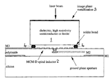
- the inductor structure comprises a chip 1 of a dielectric, high resistivity semiconductor or ferrite material that is mounted over the area of the MCM-D substrate inductor 2 by flip chip solder bonding.
- a metallisation layer 3 is defined on the upper surface of the chip 1 which gives rise to an image inductance that acts to reduce the primary inductance of the MCM-D inductor 2.
- the level of inductance reduction depends upon the separation of the layer 3 from the inductor 2 and the permeability of the material of the chip 1.
- the local removal and/or patterning of this exposed and accessible layer 3, for example by using a laser beam or other focussed energy source, can then be used to adjust the effective overall inductance of the inductor device.
- Suitable patterning structures include concentric square or circular ring patterns and spiral structures.
- Concentric ring structures provide image eddy currents that can further reduce the effective inductance in step wise manner according to the number, dimensions and location of the rings with respect to the turns of the primary inductor 2.
- the concentric ring structures may then be cut to interrupt the individual eddy currents to provide a step wise trimming action that increases the inductance.
- the effective inductance variation resulting from the use of the spiral trimming action is continuous. Trimming of such inductors may be used to tune oscillator, filter or resonator circuits.
- the upper surface metallisation layer 3 may be earthed by means of through-chip and MCM-D substrate vias if required.
- the separation of the upper metallisation layer 3 from the inductor 2, the chip to inductor gap determined by the flip chip solder bond height and the relative permittivity of the chip dielectric material will also determine the additional capacitance of this structure and the influence on the inductor self resonant frequency. For this reason low permittivity materials such as fused quartz may be preferred as the chip material.
- a suitable process for fabricating the flip chip structure involves the processing of wafers of the chip material, followed by dicing out of the individual chip components. Since the chip components have a very simple structure, the costs of fabricating them in wafer form will be extremely low.
- a wafer of the selected chip material is polished on both faces to provide a suitable surface quality for subsequent processing and use. If the material employed is a ferrite then an annealing treatment may be required after polishing to restore the original magnetic properties.
- An array of solder bump structures 4 is then defined over one face of the wafer to define the base of the chip 1. These solder bumps 4 will provide mechanical location and support and will physically separate the diced and bonded chip 1 from the MCM-D substrate surface. Corresponding solderable metallisation areas and/or solder bumps are defined on the MCM-D substrate itself.
- the solder bump structure requires a solderable metallisation layer to which the solder bump itself is wetted and which defines the area of the solder bump.
- Chromium-copper or chromium-copper-gold multilayer metallisation structures are suitable for this solderable metallisation requirement.
- the first chromium layer provides adhesion to the underlying chip surface, while an alloyed chromium-copper layer follows that provides solderability without layer dissolution (for multiple solder bump melting operations).
- the final copper or copper-plus-gold layers provide intial solderability, these metals dissolving into the solder on bump reflow and reprecipitating on cooling as intermetallic compounds of tin.
- the gold if employed, allows the solderable layer to be exposed to the atmosphere without oxidation prior to solder deposition.
- Solderable metallisation layers of this type may be defined by sequential vapour deposition through an etched metal foil or similar physical masking structure.
- the solder itself may be a tin-lead eutectic composition (63n-37Pb by wt. - melting point 183°C), but is normally a 95Pb-5Sn composition (melting point 310°C) for MCM-D applications.
- the solder may be applied by electrodeposition using a seed layer and photoresist masking scheme. Alternatively a physical masking structure may be employed with a vapour deposition process similar to that described for the solderable metallisation deposition.
- the solder may be deposited as separate layers of lead and tin or as an alloy.
- solder bumps are reflowed by heating to above the solder liquidus temperature under inert or reducing atmosphere conditions.
- Solder bump diameters between 50 and 125 micrometres are considered appropriate for the flip chip structure. Bump heights between 30 and 100micrometres are suitable.
- bump geometries are also typical for flip chip solder bonded Ics.
- a typical flip chip structure would employ four corner bumps for mechanical support.
- a preferred flip chip size would be 0.5, 1.0, 1.25, 1.5 or 2.0mm on a side.
- the inductor image metallisation layer 3 is then defined on the opposite surface of the flip chip component wafer to allow laser trimming of MCM-D inductor after dicing and mounting of the flip chip structure.
- This layer 3 may employ a variety of metallisation materials, including, for example, titanium, chromium or aluminium or some combination of such materials. No lithographic or other patterning of this layer is required at the wafer fabrication stage and indeed this layer may be deposited, for example, by sputter deposition, prior to the processing of the flip chip solder bond face. The optical reflectivity and electrical resistivity of this layer will determine the ease of laser trimming and the losses in the inductor image plane.
- the wafer After processing the wafer may be inspected and the individual flip chip components seaparated by mechanical sawing or laser scribing.
Landscapes
- Engineering & Computer Science (AREA)
- Power Engineering (AREA)
- Microelectronics & Electronic Packaging (AREA)
- Coils Or Transformers For Communication (AREA)
- Means For Warming Up And Starting Carburetors (AREA)
- Coils Of Transformers For General Uses (AREA)
- Manufacturing Cores, Coils, And Magnets (AREA)
Applications Claiming Priority (2)
| Application Number | Priority Date | Filing Date | Title |
|---|---|---|---|
| GB9415315A GB2292015B (en) | 1994-07-29 | 1994-07-29 | Trimmable inductor structure |
| GB9415315 | 1994-07-29 |
Publications (2)
| Publication Number | Publication Date |
|---|---|
| EP0694933A1 true EP0694933A1 (de) | 1996-01-31 |
| EP0694933B1 EP0694933B1 (de) | 2002-06-19 |
Family
ID=10759074
Family Applications (1)
| Application Number | Title | Priority Date | Filing Date |
|---|---|---|---|
| EP95304818A Expired - Lifetime EP0694933B1 (de) | 1994-07-29 | 1995-07-10 | Struktur einer abgleichbaren Drosselspule |
Country Status (6)
| Country | Link |
|---|---|
| US (1) | US6005466A (de) |
| EP (1) | EP0694933B1 (de) |
| JP (1) | JPH0869936A (de) |
| AT (1) | ATE219600T1 (de) |
| DE (1) | DE69527119T2 (de) |
| GB (1) | GB2292015B (de) |
Cited By (1)
| Publication number | Priority date | Publication date | Assignee | Title |
|---|---|---|---|---|
| EP0782190A3 (de) * | 1995-12-27 | 1999-06-16 | Nec Corporation | Halbleiteranordnung mit einem Induktorelement |
Families Citing this family (35)
| Publication number | Priority date | Publication date | Assignee | Title |
|---|---|---|---|---|
| US6310386B1 (en) * | 1998-12-17 | 2001-10-30 | Philips Electronics North America Corp. | High performance chip/package inductor integration |
| US6303423B1 (en) * | 1998-12-21 | 2001-10-16 | Megic Corporation | Method for forming high performance system-on-chip using post passivation process |
| US6130479A (en) * | 1999-08-02 | 2000-10-10 | International Business Machines Corporation | Nickel alloy films for reduced intermetallic formation in solder |
| US6180445B1 (en) | 2000-04-24 | 2001-01-30 | Taiwan Semiconductor Manufacturing Company | Method to fabricate high Q inductor by redistribution layer when flip-chip package is employed |
| US6856007B2 (en) * | 2001-08-28 | 2005-02-15 | Tessera, Inc. | High-frequency chip packages |
| US7176506B2 (en) * | 2001-08-28 | 2007-02-13 | Tessera, Inc. | High frequency chip packages with connecting elements |
| US7037298B2 (en) * | 2001-12-20 | 2006-05-02 | The Procter & Gamble Company | Disposable absorbent article having a raised circumferential bank |
| US7754537B2 (en) | 2003-02-25 | 2010-07-13 | Tessera, Inc. | Manufacture of mountable capped chips |
| US6972480B2 (en) | 2003-06-16 | 2005-12-06 | Shellcase Ltd. | Methods and apparatus for packaging integrated circuit devices |
| US7352070B2 (en) * | 2003-06-27 | 2008-04-01 | Delphi Technologies, Inc. | Polymer encapsulated electrical devices |
| JP2007528120A (ja) | 2003-07-03 | 2007-10-04 | テッセラ テクノロジーズ ハンガリー コルラートルト フェレロェセーギュー タールシャシャーグ | 集積回路装置をパッケージングする方法及び装置 |
| US6927663B2 (en) * | 2003-07-23 | 2005-08-09 | Cardiac Pacemakers, Inc. | Flyback transformer wire attach method to printed circuit board |
| US20050095835A1 (en) | 2003-09-26 | 2005-05-05 | Tessera, Inc. | Structure and method of making capped chips having vertical interconnects |
| US7158767B2 (en) * | 2003-10-24 | 2007-01-02 | Cts Corporation | Tuneable frequency translator |
| US7280024B2 (en) * | 2005-02-02 | 2007-10-09 | Intel Corporation | Integrated transformer structure and method of fabrication |
| US8143095B2 (en) | 2005-03-22 | 2012-03-27 | Tessera, Inc. | Sequential fabrication of vertical conductive interconnects in capped chips |
| US8384189B2 (en) | 2005-03-29 | 2013-02-26 | Megica Corporation | High performance system-on-chip using post passivation process |
| US7936062B2 (en) | 2006-01-23 | 2011-05-03 | Tessera Technologies Ireland Limited | Wafer level chip packaging |
| US7538652B2 (en) * | 2006-08-29 | 2009-05-26 | International Business Machines Corporation | Electrical component tuned by conductive layer deletion |
| US7791199B2 (en) * | 2006-11-22 | 2010-09-07 | Tessera, Inc. | Packaged semiconductor chips |
| US8569876B2 (en) * | 2006-11-22 | 2013-10-29 | Tessera, Inc. | Packaged semiconductor chips with array |
| US8604605B2 (en) | 2007-01-05 | 2013-12-10 | Invensas Corp. | Microelectronic assembly with multi-layer support structure |
| EP2135280A2 (de) | 2007-03-05 | 2009-12-23 | Tessera, Inc. | Chips mit rückseitigen kontakten, die durch durchkontaktierungen mit vorderseitigen kontakten verbunden werden |
| EP2183770B1 (de) | 2007-07-31 | 2020-05-13 | Invensas Corporation | Verfahren zur Herstellung von Substratdurchkontaktierungen und zugehöriges Bauelement |
| US9640437B2 (en) | 2010-07-23 | 2017-05-02 | Tessera, Inc. | Methods of forming semiconductor elements using micro-abrasive particle stream |
| US8791575B2 (en) | 2010-07-23 | 2014-07-29 | Tessera, Inc. | Microelectronic elements having metallic pads overlying vias |
| US8796135B2 (en) | 2010-07-23 | 2014-08-05 | Tessera, Inc. | Microelectronic elements with rear contacts connected with via first or via middle structures |
| US8847380B2 (en) | 2010-09-17 | 2014-09-30 | Tessera, Inc. | Staged via formation from both sides of chip |
| US8610259B2 (en) | 2010-09-17 | 2013-12-17 | Tessera, Inc. | Multi-function and shielded 3D interconnects |
| KR101059490B1 (ko) | 2010-11-15 | 2011-08-25 | 테세라 리써치 엘엘씨 | 임베드된 트레이스에 의해 구성된 전도성 패드 |
| US8736066B2 (en) | 2010-12-02 | 2014-05-27 | Tessera, Inc. | Stacked microelectronic assemby with TSVS formed in stages and carrier above chip |
| US8637968B2 (en) | 2010-12-02 | 2014-01-28 | Tessera, Inc. | Stacked microelectronic assembly having interposer connecting active chips |
| US8587126B2 (en) | 2010-12-02 | 2013-11-19 | Tessera, Inc. | Stacked microelectronic assembly with TSVs formed in stages with plural active chips |
| US8610264B2 (en) | 2010-12-08 | 2013-12-17 | Tessera, Inc. | Compliant interconnects in wafers |
| US20210233708A1 (en) * | 2020-01-24 | 2021-07-29 | Qorvo Us, Inc. | Inductor trimming using sacrificial magnetically coupled loops |
Citations (6)
| Publication number | Priority date | Publication date | Assignee | Title |
|---|---|---|---|---|
| JPS58196005A (ja) * | 1982-05-10 | 1983-11-15 | Toutsuu:Kk | インダクタおよびその製造方法 |
| JPS63116410A (ja) * | 1986-11-05 | 1988-05-20 | Fujikura Ltd | プリントコイルとそのインダクタンス調整方法 |
| JPH01173702A (ja) * | 1987-12-28 | 1989-07-10 | Matsushita Electric Ind Co Ltd | インダクタンス素子 |
| JPH02205309A (ja) * | 1989-02-03 | 1990-08-15 | Murata Mfg Co Ltd | インダクタ |
| EP0398485A1 (de) * | 1989-05-16 | 1990-11-22 | Gec-Marconi Limited | Verfahren zur Herstellung einer Flip-Chip-Lötstruktur für Anordnungen mit Gold-Metallisierung |
| EP0551735A1 (de) * | 1991-12-27 | 1993-07-21 | Avx Corporation | Oberflächen montierte Induktivität hoher Genauigkeit |
Family Cites Families (9)
| Publication number | Priority date | Publication date | Assignee | Title |
|---|---|---|---|---|
| GB2079066B (en) * | 1980-06-23 | 1983-09-21 | Hull Corp | Trimmable electrical inductors |
| US4494100A (en) * | 1982-07-12 | 1985-01-15 | Motorola, Inc. | Planar inductors |
| US4905358A (en) * | 1989-01-18 | 1990-03-06 | Motorola, Inc. | Thin film active trimmable capacitor/inductor |
| EP0529503A1 (de) * | 1991-08-22 | 1993-03-03 | Hewlett-Packard Company | Flip-chip-Vorrichtung mit flexibler Befestigung |
| US5239289A (en) * | 1991-09-04 | 1993-08-24 | International Business Machines Corporation | Tunable inductor |
| US5255431A (en) * | 1992-06-26 | 1993-10-26 | General Electric Company | Method of using frozen epoxy for placing pin-mounted components in a circuit module |
| US5502667A (en) * | 1993-09-13 | 1996-03-26 | International Business Machines Corporation | Integrated multichip memory module structure |
| GB2290913B (en) * | 1994-06-30 | 1998-03-11 | Plessey Semiconductors Ltd | Multi-chip module inductor structure |
| US5534837A (en) * | 1994-07-28 | 1996-07-09 | Rockwell International | Orthogonal-field electrically variable magnetic device |
-
1994
- 1994-07-29 GB GB9415315A patent/GB2292015B/en not_active Expired - Fee Related
-
1995
- 1995-07-10 AT AT95304818T patent/ATE219600T1/de not_active IP Right Cessation
- 1995-07-10 EP EP95304818A patent/EP0694933B1/de not_active Expired - Lifetime
- 1995-07-10 DE DE69527119T patent/DE69527119T2/de not_active Expired - Fee Related
- 1995-07-24 US US08/506,317 patent/US6005466A/en not_active Expired - Fee Related
- 1995-07-25 JP JP7209221A patent/JPH0869936A/ja active Pending
Patent Citations (6)
| Publication number | Priority date | Publication date | Assignee | Title |
|---|---|---|---|---|
| JPS58196005A (ja) * | 1982-05-10 | 1983-11-15 | Toutsuu:Kk | インダクタおよびその製造方法 |
| JPS63116410A (ja) * | 1986-11-05 | 1988-05-20 | Fujikura Ltd | プリントコイルとそのインダクタンス調整方法 |
| JPH01173702A (ja) * | 1987-12-28 | 1989-07-10 | Matsushita Electric Ind Co Ltd | インダクタンス素子 |
| JPH02205309A (ja) * | 1989-02-03 | 1990-08-15 | Murata Mfg Co Ltd | インダクタ |
| EP0398485A1 (de) * | 1989-05-16 | 1990-11-22 | Gec-Marconi Limited | Verfahren zur Herstellung einer Flip-Chip-Lötstruktur für Anordnungen mit Gold-Metallisierung |
| EP0551735A1 (de) * | 1991-12-27 | 1993-07-21 | Avx Corporation | Oberflächen montierte Induktivität hoher Genauigkeit |
Non-Patent Citations (4)
| Title |
|---|
| PATENT ABSTRACTS OF JAPAN vol. 008, no. 036 (E - 227) 16 February 1984 (1984-02-16) * |
| PATENT ABSTRACTS OF JAPAN vol. 012, no. 362 (E - 663) 28 September 1988 (1988-09-28) * |
| PATENT ABSTRACTS OF JAPAN vol. 013, no. 445 (E - 829) 6 October 1989 (1989-10-06) * |
| PATENT ABSTRACTS OF JAPAN vol. 014, no. 496 (E - 0996) 29 October 1990 (1990-10-29) * |
Cited By (1)
| Publication number | Priority date | Publication date | Assignee | Title |
|---|---|---|---|---|
| EP0782190A3 (de) * | 1995-12-27 | 1999-06-16 | Nec Corporation | Halbleiteranordnung mit einem Induktorelement |
Also Published As
| Publication number | Publication date |
|---|---|
| GB2292015B (en) | 1998-07-22 |
| GB9415315D0 (en) | 1994-09-21 |
| EP0694933B1 (de) | 2002-06-19 |
| GB2292015A (en) | 1996-02-07 |
| ATE219600T1 (de) | 2002-07-15 |
| DE69527119D1 (de) | 2002-07-25 |
| US6005466A (en) | 1999-12-21 |
| DE69527119T2 (de) | 2003-01-16 |
| JPH0869936A (ja) | 1996-03-12 |
Similar Documents
| Publication | Publication Date | Title |
|---|---|---|
| EP0694933B1 (de) | Struktur einer abgleichbaren Drosselspule | |
| EP0685857B1 (de) | Chip-induktivität Anordnung | |
| US5747870A (en) | Multi-chip module inductor structure | |
| US5892287A (en) | Semiconductor device including stacked chips having metal patterned on circuit surface and on edge side of chip | |
| EP2159916B1 (de) | Abzweigfilter und Verfahren zu seiner Herstellung | |
| US8043896B2 (en) | Semiconductor chip, method of manufacturing the semiconductor chip and semiconductor chip package including an inclined via hole | |
| CN101611494B (zh) | 具有电感衬底的芯片级功率转换器封装 | |
| US7816787B2 (en) | Method of forming low stress multi-layer metallurgical structures and high reliable lead free solder termination electrodes | |
| US20030162386A1 (en) | Semiconductor device and its manufacturing method | |
| US5561328A (en) | Photo-definable template for semiconductor chip alignment | |
| US6841877B2 (en) | Semiconductor device, metal laminated plate for fabricating circuit on semiconductor, and method of fabricating circuit | |
| US6946321B1 (en) | Method of forming the integrated circuit having a die with high Q inductors and capacitors attached to a die with a circuit as a flip chip | |
| US6069026A (en) | Semiconductor device and method of fabrication | |
| EP0694932B1 (de) | Drosselspuleanordnung | |
| US5072873A (en) | Device for solder removal | |
| US6159817A (en) | Multi-tap thin film inductor | |
| JP2002033239A (ja) | Lcフィルタ | |
| US11056555B2 (en) | Semiconductor device having 3D inductor and method of manufacturing the same | |
| CN110739236A (zh) | 一种具有防溢锡结构的新三维异构堆叠方法 | |
| US6338973B1 (en) | Semiconductor device and method of fabrication | |
| US6372623B1 (en) | Semiconductor device and method of fabrication | |
| GB2079066A (en) | Trimmable electrical inductors | |
| US20240105390A1 (en) | Device and process for implementing silicon carbide (sic) surface mount devices | |
| CN119153232B (zh) | 电容芯片结构以及制造方法 | |
| US20250174588A1 (en) | Method of manufacturing electronic components with wettable flanks |
Legal Events
| Date | Code | Title | Description |
|---|---|---|---|
| PUAI | Public reference made under article 153(3) epc to a published international application that has entered the european phase |
Free format text: ORIGINAL CODE: 0009012 |
|
| AK | Designated contracting states |
Kind code of ref document: A1 Designated state(s): AT DE ES FR GB IT |
|
| 17P | Request for examination filed |
Effective date: 19960716 |
|
| RAP1 | Party data changed (applicant data changed or rights of an application transferred) |
Owner name: MITEL SEMICONDUCTOR LIMITED |
|
| 17Q | First examination report despatched |
Effective date: 19981208 |
|
| RAP1 | Party data changed (applicant data changed or rights of an application transferred) |
Owner name: INTARSIA CORPORATION |
|
| GRAG | Despatch of communication of intention to grant |
Free format text: ORIGINAL CODE: EPIDOS AGRA |
|
| GRAG | Despatch of communication of intention to grant |
Free format text: ORIGINAL CODE: EPIDOS AGRA |
|
| GRAH | Despatch of communication of intention to grant a patent |
Free format text: ORIGINAL CODE: EPIDOS IGRA |
|
| GRAH | Despatch of communication of intention to grant a patent |
Free format text: ORIGINAL CODE: EPIDOS IGRA |
|
| GRAA | (expected) grant |
Free format text: ORIGINAL CODE: 0009210 |
|
| AK | Designated contracting states |
Kind code of ref document: B1 Designated state(s): AT DE ES FR GB IT |
|
| PG25 | Lapsed in a contracting state [announced via postgrant information from national office to epo] |
Ref country code: AT Free format text: LAPSE BECAUSE OF FAILURE TO SUBMIT A TRANSLATION OF THE DESCRIPTION OR TO PAY THE FEE WITHIN THE PRESCRIBED TIME-LIMIT Effective date: 20020619 |
|
| REF | Corresponds to: |
Ref document number: 219600 Country of ref document: AT Date of ref document: 20020715 Kind code of ref document: T |
|
| REG | Reference to a national code |
Ref country code: GB Ref legal event code: FG4D |
|
| REF | Corresponds to: |
Ref document number: 69527119 Country of ref document: DE Date of ref document: 20020725 |
|
| PGFP | Annual fee paid to national office [announced via postgrant information from national office to epo] |
Ref country code: GB Payment date: 20020904 Year of fee payment: 8 |
|
| PGFP | Annual fee paid to national office [announced via postgrant information from national office to epo] |
Ref country code: FR Payment date: 20020930 Year of fee payment: 8 Ref country code: DE Payment date: 20020930 Year of fee payment: 8 |
|
| ET | Fr: translation filed | ||
| PG25 | Lapsed in a contracting state [announced via postgrant information from national office to epo] |
Ref country code: ES Free format text: LAPSE BECAUSE OF FAILURE TO SUBMIT A TRANSLATION OF THE DESCRIPTION OR TO PAY THE FEE WITHIN THE PRESCRIBED TIME-LIMIT Effective date: 20021220 |
|
| PLBE | No opposition filed within time limit |
Free format text: ORIGINAL CODE: 0009261 |
|
| STAA | Information on the status of an ep patent application or granted ep patent |
Free format text: STATUS: NO OPPOSITION FILED WITHIN TIME LIMIT |
|
| 26N | No opposition filed |
Effective date: 20030320 |
|
| PG25 | Lapsed in a contracting state [announced via postgrant information from national office to epo] |
Ref country code: GB Free format text: LAPSE BECAUSE OF NON-PAYMENT OF DUE FEES Effective date: 20030710 |
|
| PG25 | Lapsed in a contracting state [announced via postgrant information from national office to epo] |
Ref country code: DE Free format text: LAPSE BECAUSE OF NON-PAYMENT OF DUE FEES Effective date: 20040203 |
|
| GBPC | Gb: european patent ceased through non-payment of renewal fee |
Effective date: 20030710 |
|
| PG25 | Lapsed in a contracting state [announced via postgrant information from national office to epo] |
Ref country code: FR Free format text: LAPSE BECAUSE OF NON-PAYMENT OF DUE FEES Effective date: 20040331 |
|
| REG | Reference to a national code |
Ref country code: FR Ref legal event code: ST |
|
| PG25 | Lapsed in a contracting state [announced via postgrant information from national office to epo] |
Ref country code: IT Free format text: LAPSE BECAUSE OF NON-PAYMENT OF DUE FEES Effective date: 20050710 |