EP0697649A2 - Struktur und Verfahren zum Verschieben und Wiedereinordnen einer Vielzahl von Datenbytes - Google Patents
Struktur und Verfahren zum Verschieben und Wiedereinordnen einer Vielzahl von Datenbytes Download PDFInfo
- Publication number
- EP0697649A2 EP0697649A2 EP95111691A EP95111691A EP0697649A2 EP 0697649 A2 EP0697649 A2 EP 0697649A2 EP 95111691 A EP95111691 A EP 95111691A EP 95111691 A EP95111691 A EP 95111691A EP 0697649 A2 EP0697649 A2 EP 0697649A2
- Authority
- EP
- European Patent Office
- Prior art keywords
- multiplexers
- buses
- byte
- shifting
- data bytes
- Prior art date
- Legal status (The legal status is an assumption and is not a legal conclusion. Google has not performed a legal analysis and makes no representation as to the accuracy of the status listed.)
- Granted
Links
Images


Classifications
-
- G—PHYSICS
- G06—COMPUTING OR CALCULATING; COUNTING
- G06F—ELECTRIC DIGITAL DATA PROCESSING
- G06F7/00—Methods or arrangements for processing data by operating upon the order or content of the data handled
- G06F7/76—Arrangements for rearranging, permuting or selecting data according to predetermined rules, independently of the content of the data
- G06F7/762—Arrangements for rearranging, permuting or selecting data according to predetermined rules, independently of the content of the data having at least two separately controlled rearrangement levels, e.g. multistage interconnection networks
Definitions
- the present invention relates to shifter circuitry for use in a data processing system.
- the present invention relates to a structure and method for independently shifting a plurality of bytes in a data processing system.
- shifter circuitry has been used to shift a plurality of data bytes.
- Prior art shifters typically utilize barrel shifter circuitry to allow a plurality of bytes to be shifted by a fixed number of bits. That is, all bytes are shifted in the same direction by the same number of bits.
- a shifter circuit is provided to independently shift and/or reorder a plurality of data bytes.
- This shifter circuit includes first and second registers which each receive a plurality of data bytes.
- the first register is coupled to a plurality of first buses, with each of the first buses receiving a data byte from the first register.
- the second register is coupled to a plurality of second buses, with each of the second buses receiving a data byte from the second register.
- a multiplicity of third buses are coupled to the first and second buses.
- Byte shifting multiplexers are coupled to each of the third buses.
- a plurality of bit shifting multiplexers are coupled to the byte shifting multiplexers, with each bit shifting multiplexer being coupled to a pair of byte shifting multiplexers.
- a control circuit is coupled to the byte shifting and bit shifting multiplexers. The control circuit provides for independent control of each of the byte shifting multiplexers. The control circuit also provides for independent control of each of the bit shifting multiplexers.
- a first multiplexer is coupled to each of the first buses and a second multiplexer is coupled to each of the second buses.
- a multiplicity of intermediate multiplexers are each coupled to at least one of the first buses and at least one of the second buses.
- a control circuit is coupled to the first, second and intermediate multiplexers to control the routing of the data bytes.
- the control circuit independently controls each of the first, second and intermediate multiplexers, such that these multiplexers can simultaneously perform shifting and reordering of the data bytes. This advantageously increases the speed of the shifter circuit.
- the shifter circuit also eliminates the need for separate byte shifting and reordering circuitry, thereby reducing the layout area of the shifter circuit.
- the shifter circuit includes a plurality of bit shifting multiplexers coupled to the first, second and intermediate multiplexers and to the control circuitry. Each of the bit shifting multiplexers is independently controlled by the control circuitry.
- Fig. 1 is a block diagram illustrating one embodiment of shifter circuit 100 in accordance with one embodiment of the present invention.
- Shifter circuit 100 has two 72-bit input registers 101 and 102.
- Input register 101 receives a 72-bit input IL[71:0] which includes eight 9-bit bytes.
- Input IL[71:0] is ordered from a most significant byte, IL[71:63], to an intermediate significance byte, IL[8:0].
- Input register 102 receives a 72-bit input IR[71:0] which also includes eight 9-bit bytes.
- Input IR[71:0] is ordered from an intermediate significance byte IR[71:63], to a least significant byte, IR[8:0].
- Input register 101 is coupled to eight output buses 111-118. Each of buses 111-118 carries a 9-bit byte. Nine-bit bus 111 carries most significant byte IL[71:63] and 9-bit bus 118 carries intermediate significance byte IL[8:0].
- input register 102 is coupled to eight output buses 121-128.
- buses 121-128 carries a 9-bit byte.
- Nine-bit bus 121 carries intermediate significance byte IR[71:63] and 9-bit bus 128 carries least significant byte IR[8:0].
- Bus 131 couples each of 9-bit buses 111-118 to multiplexer 11.
- Multiplexer 11 is an 8-to-1 multiplexer which passes one of the bytes from 9-bit buses 111-118.
- Multiplexers 12-26 are 8-to-1 multiplexers similar to multiplexer 11.
- Buses 132 and 133 couple 9-bit buses 112-118 and 121 to multiplexers 12 and 13, respectively.
- Buses 134 and 135 couple 9-bit buses 113-118 and 121-122 to multiplexers 14 and 15, respectively.
- Buses 136 and 137 couple 9-bit buses 114-118 and 121-123 to multiplexers 16 and 17, respectively.
- Buses 138 and 139 couple 9-bit buses 115-118 and 121-124 to multiplexers 18 and 19, respectively.
- Buses 140 and 141 couple 9-bit buses 116-118 and 121-125 to multiplexers 20 and 21, respectively.
- Buses 142 and 143 couple 9-bit buses 117-118 and 121-126 to multiplexers 22 and 23, respectively.
- Buses 144 and 145 couple 9-bit buses 118 and 121-127 to multiplexers 24 and 25, respectively.
- Bus 146 couples 9-bit buses 121-128 to multiplexer 26.
- Each of multiplexers 11-26 pass a 9-bit byte, thereby creating two 72-bit outputs, OL[71:0] and OR[71:0].
- Each byte of OL[71:0] is selected from one of eight adjacent bytes of the 16-byte concatenation of inputs IL[71:0] and IR[71:0].
- the most significant byte OL[71:63] of output OL[71:0] is selected from one of the 8 bytes on buses 111-118.
- the second most significant byte OL[62:54] is selected from one of the eight bytes on buses 112-118 and 121.
- the least significant byte OL[8:0] is selected from one of the eight bytes on buses 118 and 121-127.
- Each of multiplexers 11-26 is independently controlled. As a result, bytes from registers 101 and 102 can be reordered and shifted to perform data packing and unpacking. In one embodiment, the sixteen input bytes in registers 101 and 102 are packed into and out of two dimensional formats.
- Shifter circuit 100 optionally employs multiplexers 1-8 to perform a bit shifting operation.
- Multiplexers 1, 2, 3, 4, 5, 6, 7 and 8 receive inputs from multiplexer pairs 11-12, 13-14, 15-16, 17-18, 19-20, 21-22, 23-24 and 25-26, respectively.
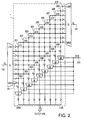
- Fig. 2 is a block diagram of multiplexer 1 in accordance with one embodiment of the present invention.
- multiplexers 2-8 are similar to multiplexer 1.
- Multiplexer 1 receives the 9-bit output OL[71:63] from multiplexer 11 and the 9-bit output OR[71:63] from multiplexer 12.
- the 9-bits of output OL[71:63] are provided from multiplexer 11 on buses 201-209, with bus 201 carrying the most significant bit and bus 209 carrying the least significant bit.
- the 9-bits of output OR[71:63] are provided from multiplexer 12 on buses 211-219, with bus 211 carrying the most significant bit and bus 219 carrying the least significant bit.
- Multiplexers 31-39 are 10-to-1 multiplexers.
- Multiplexer 31 is coupled to buses 201-209 and 211.
- Multiplexer 32 is coupled to buses 202-209 and 211-212.
- Multiplexer 33 is coupled to buses 203-209 and 211-213.
- Multiplexer 34 is coupled to buses 204-209 and 211-214.
- Multiplexer 35 is coupled to buses 205-209 and 211-215.
- Multiplexer 36 is coupled to buses 206-209 and 211-216.
- Multiplexer 37 is coupled to buses 207-209 and 211-217.
- Multiplexer 38 is coupled to buses 208-209 and 211-218.
- Multiplexer 39 is coupled to buses 209 and 211-219.
- Each of multiplexers 31-39 receives a 4-bit control signal C[3:0] on bus 230 to select the bits of output byte OUT[71:63].
- Output byte OUT[71:63] consists of 9 consecutive bits of the 18-bit concatenation of OL[71:63] and OR[71:63].
- Multiplexers 2, 3, 4, 5, 6, 7 and 8 operate in a manner similar to multiplexer 1 to create outputs OUT[62:54], OUT[53:45], OUT[44:36], OUT[35:27], OUT[26:18], OUT[17:9] and OUT[8:0], respectively.
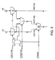
- Fig. 3 is a schematic diagram which illustrates the control of multiplexers 1, 11 and 12 in accordance with one embodiment of the present invention.
- a 9-bit control signal, CTRL[71:63] and multiplexers 300 and 301 are used to control the operation of multiplexers 1, 11 and 12.
- control bits CTRL[71:68] are provided to multiplexer 11.
- multiplexer 11 passes the desired byte (i.e., OL[71:63]) from bus 131 through multiplexer 11.
- Control bit CTRL[63] is provided to multiplexer 301, such that multiplexer 301 passes control bits CTRL[67:64] to multiplexer 12.
- multiplexer 12 passes the desired byte (i.e., OR[71:63]) from bus 132 through multiplexer 12.
- Control bit CTRL[63] is also provided to multiplexer 300.
- multiplexer 300 passes the output of multiplexer 11 (i.e., OL[71:63]) through multiplexer 300.
- control bits CTRL[71:68] are provided to multiplexer 11.
- Control bit CTRL[63] is selected such that multiplexer 301 transmits control bits CTRL[71:68] to multiplexer 12.
- multiplexers 11 and 12 receive the same four control bits. Because the eight bytes input to multiplexers 11 and 12 are offset by one byte, the application of the same control bits to multiplexers 11 and 12 results in the selection of consecutive bytes. Table 1 below sets forth one embodiment of the consecutive bytes which can be selected by control bits CTRL[71:68].
- Multiplexer 1 receives control bits CTRL[67:64] and in response, performs the bit shifting function previously described in connection with Fig. 2.
- the bits passed through multiplexer 1 i.e., OUT[71:63]
- multiplexer 300 passes the output byte OUT[71:63].
- Multiplexers 2-8 and 12-26 are controlled in a manner similar to multiplexers 1, 11 and 12.
- multiplexers 2, 13 and 14 are controlled by control bits CTRL[62:54]
- multiplexers 3, 15 and 16 are controlled by control bits CTRL[53:45]
- multiplexers 4, 17 and 18 are controlled by control bits CTRL[44:36]
- multiplexers 5, 19 and 20 are controlled by control bits CTRL[35:27]
- multiplexers 6, 21 and 22 are controlled by control bits CTRL[26:18]
- multiplexers 7, 23 and 24 are controlled by control bits CTRL[17:9]
- multiplexers 8, 25 and 26 are controlled by control bits CTRL[8:0].
- multiplexers 1-8 and 11-26 are controlled by a 72-bit control signal CTRL[71:0].
- multiplexers 1-8 and 11-26 are operated from the same control signal, the byte shifting and reordering functions performed by multiplexers 11-26 and the bit shifting function performed by multiplexers 1-8 can be executed in one clock cycle. This advantageously increases the speed of shifter circuit 100. Shifter circuit 100 also eliminates the need for separate byte shifting and reordering circuitry, thereby reducing the layout area of shifter circuit 100.
- control circuit is modified to allow for independent control of the bytes passed through multiplexers 11-26 during a bit shifting operation. That is, any of the bytes applied to multiplexers 11-26 (not just consecutive bytes) can be passed through multiplexers 11-26 during a bit shifting operation.
- the modified control circuit requires eighty bits: three bits to control each of multiplexers 11-26 and four bits to control each of multiplexers 1-8.
- Fig. 4 is a schematic diagram of a shifter circuit 400 in accordance with an alternate embodiment of the present invention. Because shifter circuit 400 is similar to shifter circuit 100 (Fig. 1), similar elements in shifter circuits 100 and 400 are labeled with similar numbers.
- Each of buses 431-446 receive all sixteen 9-bit bytes from registers 101 and 102. Hence, each of buses 431-446 is 144 bits wide and carries sixteen bytes of information.
- Multiplexers 41-56 are 16-to-1 multiplexers.
- the same decoder circuitry illustrated in Fig. 3 is utilized in shifter circuit 400.
- multiplexers 41 and 42 can be substituted for multiplexers 11 and 12 in Fig. 3. Because multiplexers 11 and 12 (Fig. 3) are controlled with four control bits CTRL[71:68], the associated control circuitry is capable of decoding up to sixteen combinations of consecutive bytes. Table 2 below sets forth one embodiment of the consecutive bytes which can be passed through multiplexers 41 and 42 in response to control bits CTRL[71:68] in shifter circuit 400. Because each of multiplexers 41-56 in shifter circuit 400 receive the same sixteen bytes from registers 101 and 102, Table 2 is applicable to each of multiplexers 41-56.
- shifter circuit 400 is capable of performing the byte shifting and reordering functions and the bit shifting function in the same clock cycle. As previously discussed, this increases the speed and reduces the layout area of shifter circuit 400.
- a shifter circuit and method for simultaneously and independently shifting and reordering a plurality of data bytes includes first and second registers which each receive a plurality of data bytes.
- the first register is coupled to a plurality of first buses, with each of the first buses receiving a data byte from the first register.
- the second register is coupled to a plurality of second buses, with each of the second buses receiving a data byte from the second register.
- a multiplicity of third buses are coupled to the first and second buses.
- a byte shifting multiplexer is coupled to each of the third buses.
- a plurality of bit shifting multiplexer are coupled to the byte shifting multiplexers, with each bit shifting multiplexer being coupled to a pair of byte shifting multiplexers.
- a control circuit is coupled to the byte shifting and bit shifting multiplexers. The control circuit provides for independent control of each of the byte shifting multiplexers. The control circuit also provides for independent control of each of the bit shifting multiplexers.
Landscapes
- Engineering & Computer Science (AREA)
- Theoretical Computer Science (AREA)
- Physics & Mathematics (AREA)
- General Engineering & Computer Science (AREA)
- General Physics & Mathematics (AREA)
- Bus Control (AREA)
- Logic Circuits (AREA)
- Electronic Switches (AREA)
Applications Claiming Priority (2)
| Application Number | Priority Date | Filing Date | Title |
|---|---|---|---|
| US285379 | 1994-08-03 | ||
| US08/285,379 US5477543A (en) | 1994-08-03 | 1994-08-03 | Structure and method for shifting and reordering a plurality of data bytes |
Publications (3)
| Publication Number | Publication Date |
|---|---|
| EP0697649A2 true EP0697649A2 (de) | 1996-02-21 |
| EP0697649A3 EP0697649A3 (de) | 1996-05-01 |
| EP0697649B1 EP0697649B1 (de) | 1999-11-10 |
Family
ID=23093985
Family Applications (1)
| Application Number | Title | Priority Date | Filing Date |
|---|---|---|---|
| EP95111691A Expired - Lifetime EP0697649B1 (de) | 1994-08-03 | 1995-07-25 | Struktur und Verfahren zum Verschieben und Wiedereinordnen einer Vielzahl von Datenbytes |
Country Status (4)
| Country | Link |
|---|---|
| US (1) | US5477543A (de) |
| EP (1) | EP0697649B1 (de) |
| JP (1) | JP3445416B2 (de) |
| DE (1) | DE69513243T2 (de) |
Families Citing this family (22)
| Publication number | Priority date | Publication date | Assignee | Title |
|---|---|---|---|---|
| US6275834B1 (en) * | 1994-12-01 | 2001-08-14 | Intel Corporation | Apparatus for performing packed shift operations |
| US6738793B2 (en) * | 1994-12-01 | 2004-05-18 | Intel Corporation | Processor capable of executing packed shift operations |
| ZA9510127B (en) * | 1994-12-01 | 1996-06-06 | Intel Corp | Novel processor having shift operations |
| US6643765B1 (en) * | 1995-08-16 | 2003-11-04 | Microunity Systems Engineering, Inc. | Programmable processor with group floating point operations |
| US5638533A (en) * | 1995-10-12 | 1997-06-10 | Lsi Logic Corporation | Method and apparatus for providing data to a parallel processing array |
| US5978822A (en) * | 1995-12-29 | 1999-11-02 | Atmel Corporation | Circuit for rotating, left shifting, or right shifting bits |
| US5784011A (en) * | 1996-06-14 | 1998-07-21 | Lsi Logic Corporation | Multiplier circuit for performing inverse quantization arithmetic |
| DE19653568A1 (de) * | 1996-12-20 | 1997-07-10 | Bernd Paysan | Zugriffsnetzwerk zur Adressierung von Teilwörtern für aufsteigende und absteigende Byte-Reihenfolge im Speicher |
| WO2000074058A1 (en) * | 1999-05-28 | 2000-12-07 | Hitachi, Ltd. | Storage, storage method, and data processing system |
| US6629115B1 (en) * | 1999-10-01 | 2003-09-30 | Hitachi, Ltd. | Method and apparatus for manipulating vectored data |
| US6643673B1 (en) | 1999-11-30 | 2003-11-04 | Ati International, Srl | Method and apparatus for arithmetic shifting |
| US6675181B1 (en) * | 1999-12-23 | 2004-01-06 | Ati International, Srl | Method and apparatus for determining a byte select vector for a crossbar shifter |
| US6816593B1 (en) * | 1999-12-23 | 2004-11-09 | Ati International Srl | Method and apparatus for transposing bits |
| US6850338B1 (en) | 2000-05-12 | 2005-02-01 | International Business Machines Corporation | Method, system, program, and data structure for generating raster objects |
| US6894796B1 (en) | 2000-05-12 | 2005-05-17 | International Business Machines Corporation | Method, system, and logic for selecting line work and control data for a pixel from multiple objects of line work data provided for the pixel |
| US7394568B1 (en) | 2000-05-15 | 2008-07-01 | Infoprint Solutions Company Llc | Method, system, and logic for selecting pixel data from multiple objects |
| US6449328B1 (en) | 2000-05-15 | 2002-09-10 | International Business Machines Corporation | Method and apparatus for shifting data from registers |
| US6804411B1 (en) | 2000-05-15 | 2004-10-12 | International Business Machines Corporation | Method, system, and program for decompressing and aligning line work data from multiple objects |
| US6961134B1 (en) | 2000-05-15 | 2005-11-01 | International Business Machines Corporation | Method, system, and logic using multiplexers to select data for pixels from multiple objects |
| US6993028B2 (en) * | 2001-07-13 | 2006-01-31 | Integrated Device Technology, Inc. | Apparatus and method for reordering sequence indicated information units into proper sequence |
| JP3415126B2 (ja) * | 2001-09-04 | 2003-06-09 | 三菱電機株式会社 | 可変長符号多重化装置、可変長符号分離装置、可変長符号多重化方法及び可変長符号分離方法 |
| GB2443439B (en) * | 2006-10-30 | 2009-06-03 | Imagination Tech Ltd | Digital electronic binary rotator and reverser |
Family Cites Families (7)
| Publication number | Priority date | Publication date | Assignee | Title |
|---|---|---|---|---|
| US4512018A (en) * | 1983-03-08 | 1985-04-16 | Burroughs Corporation | Shifter circuit |
| JPH0650462B2 (ja) * | 1986-02-18 | 1994-06-29 | 日本電気株式会社 | シフト数制御回路 |
| DE3633302A1 (de) * | 1986-09-30 | 1988-03-31 | Siemens Ag | Schaltungsanordnung zum auswaehlen und/oder ausrichten von dateneinheiten in datenverarbeitungsanlagen |
| JPS6428752A (en) * | 1987-07-24 | 1989-01-31 | Toshiba Corp | Data processor |
| JPH0225921A (ja) * | 1988-07-15 | 1990-01-29 | Toshiba Corp | バレルシフタ |
| CA2050799C (en) * | 1990-09-07 | 1994-03-22 | Shingo Ishihara | Shift amount floating-point calculating circuit with a small amount of hardware and rapidly operable |
| EP0522186B1 (de) * | 1991-07-06 | 1996-10-23 | International Business Machines Corporation | Multiplexer |
-
1994
- 1994-08-03 US US08/285,379 patent/US5477543A/en not_active Expired - Lifetime
-
1995
- 1995-07-25 DE DE69513243T patent/DE69513243T2/de not_active Expired - Lifetime
- 1995-07-25 EP EP95111691A patent/EP0697649B1/de not_active Expired - Lifetime
- 1995-08-02 JP JP21670995A patent/JP3445416B2/ja not_active Expired - Lifetime
Non-Patent Citations (1)
| Title |
|---|
| None |
Also Published As
| Publication number | Publication date |
|---|---|
| EP0697649B1 (de) | 1999-11-10 |
| JP3445416B2 (ja) | 2003-09-08 |
| EP0697649A3 (de) | 1996-05-01 |
| JPH08212053A (ja) | 1996-08-20 |
| US5477543A (en) | 1995-12-19 |
| DE69513243T2 (de) | 2000-03-30 |
| DE69513243D1 (de) | 1999-12-16 |
Similar Documents
| Publication | Publication Date | Title |
|---|---|---|
| US5477543A (en) | Structure and method for shifting and reordering a plurality of data bytes | |
| CA1175154A (en) | Shift circuit | |
| JP3295077B2 (ja) | ビデオプロセッサシステム | |
| US6381690B1 (en) | Processor for performing subword permutations and combinations | |
| CA1208793A (en) | Staging memory for massively parallel processor | |
| US4467422A (en) | Array processor | |
| EP0751456A1 (de) | Effiziente Wahl und Mischung von mehreren, in zwei oder mehr Computerwörter gepackten Sub-Wortteilen | |
| US5309382A (en) | Binary shifter | |
| JPH0284689A (ja) | ビデオメモリ装置 | |
| KR960005102B1 (ko) | 배럴시프터 | |
| US4631703A (en) | Shift circuit for double word length data | |
| EP0522186B1 (de) | Multiplexer | |
| US4512018A (en) | Shifter circuit | |
| EP0025323A2 (de) | Schiebeschaltung | |
| JPH0327635A (ja) | デイジタル通信装置 | |
| US4935737A (en) | Data selection matrix | |
| EP0350966B1 (de) | Multipositionsverschieber | |
| US5987488A (en) | Matrix processor | |
| US5987090A (en) | Method and apparatus for a logarithmic shift register | |
| KR100205351B1 (ko) | 반도체 기억 장치의 주소 정렬 장치 | |
| JPS62182857A (ja) | 入出力制御装置 | |
| US7353371B2 (en) | Circuit to extract nonadjacent bits from data packets | |
| US6993017B1 (en) | Switch apparatus | |
| JP3023721B2 (ja) | Srm間ハイウエイ接続方法および装置 | |
| US6262750B1 (en) | Process for storing cues with different formats in a memory and corresponding storage and reading device |
Legal Events
| Date | Code | Title | Description |
|---|---|---|---|
| PUAI | Public reference made under article 153(3) epc to a published international application that has entered the european phase |
Free format text: ORIGINAL CODE: 0009012 |
|
| AK | Designated contracting states |
Kind code of ref document: A2 Designated state(s): DE FR GB IT |
|
| PUAL | Search report despatched |
Free format text: ORIGINAL CODE: 0009013 |
|
| AK | Designated contracting states |
Kind code of ref document: A3 Designated state(s): DE FR GB IT |
|
| 17P | Request for examination filed |
Effective date: 19961004 |
|
| 17Q | First examination report despatched |
Effective date: 19980326 |
|
| GRAG | Despatch of communication of intention to grant |
Free format text: ORIGINAL CODE: EPIDOS AGRA |
|
| GRAG | Despatch of communication of intention to grant |
Free format text: ORIGINAL CODE: EPIDOS AGRA |
|
| GRAH | Despatch of communication of intention to grant a patent |
Free format text: ORIGINAL CODE: EPIDOS IGRA |
|
| GRAH | Despatch of communication of intention to grant a patent |
Free format text: ORIGINAL CODE: EPIDOS IGRA |
|
| GRAA | (expected) grant |
Free format text: ORIGINAL CODE: 0009210 |
|
| RAP1 | Party data changed (applicant data changed or rights of an application transferred) |
Owner name: ATI INTERNATIONAL SRL |
|
| AK | Designated contracting states |
Kind code of ref document: B1 Designated state(s): DE FR GB IT |
|
| REF | Corresponds to: |
Ref document number: 69513243 Country of ref document: DE Date of ref document: 19991216 |
|
| ITF | It: translation for a ep patent filed | ||
| ET | Fr: translation filed | ||
| PLBE | No opposition filed within time limit |
Free format text: ORIGINAL CODE: 0009261 |
|
| STAA | Information on the status of an ep patent application or granted ep patent |
Free format text: STATUS: NO OPPOSITION FILED WITHIN TIME LIMIT |
|
| 26N | No opposition filed | ||
| REG | Reference to a national code |
Ref country code: GB Ref legal event code: IF02 |
|
| PG25 | Lapsed in a contracting state [announced via postgrant information from national office to epo] |
Ref country code: IT Free format text: LAPSE BECAUSE OF NON-PAYMENT OF DUE FEES Effective date: 20050725 |
|
| REG | Reference to a national code |
Ref country code: GB Ref legal event code: 732E Free format text: REGISTERED BETWEEN 20091231 AND 20100106 |
|
| PGRI | Patent reinstated in contracting state [announced from national office to epo] |
Ref country code: IT Effective date: 20091201 |
|
| REG | Reference to a national code |
Ref country code: FR Ref legal event code: TP |
|
| PGFP | Annual fee paid to national office [announced via postgrant information from national office to epo] |
Ref country code: FR Payment date: 20130724 Year of fee payment: 19 |
|
| PGFP | Annual fee paid to national office [announced via postgrant information from national office to epo] |
Ref country code: IT Payment date: 20130718 Year of fee payment: 19 |
|
| PGFP | Annual fee paid to national office [announced via postgrant information from national office to epo] |
Ref country code: DE Payment date: 20140724 Year of fee payment: 20 |
|
| PGFP | Annual fee paid to national office [announced via postgrant information from national office to epo] |
Ref country code: GB Payment date: 20140723 Year of fee payment: 20 |
|
| REG | Reference to a national code |
Ref country code: FR Ref legal event code: ST Effective date: 20150331 |
|
| PG25 | Lapsed in a contracting state [announced via postgrant information from national office to epo] |
Ref country code: IT Free format text: LAPSE BECAUSE OF NON-PAYMENT OF DUE FEES Effective date: 20140725 |
|
| PG25 | Lapsed in a contracting state [announced via postgrant information from national office to epo] |
Ref country code: FR Free format text: LAPSE BECAUSE OF NON-PAYMENT OF DUE FEES Effective date: 20140731 |
|
| REG | Reference to a national code |
Ref country code: DE Ref legal event code: R071 Ref document number: 69513243 Country of ref document: DE |
|
| REG | Reference to a national code |
Ref country code: GB Ref legal event code: PE20 Expiry date: 20150724 |
|
| PG25 | Lapsed in a contracting state [announced via postgrant information from national office to epo] |
Ref country code: GB Free format text: LAPSE BECAUSE OF EXPIRATION OF PROTECTION Effective date: 20150724 |