EP0697719A2 - Mikroelektronische Struktur mit einer Sperrschicht aus leitendem exotischen Nitrid für Elektroden mit einer hohen Dielektrizitätskonstante und Verfahren zu deren Herstellung - Google Patents
Mikroelektronische Struktur mit einer Sperrschicht aus leitendem exotischen Nitrid für Elektroden mit einer hohen Dielektrizitätskonstante und Verfahren zu deren Herstellung Download PDFInfo
- Publication number
- EP0697719A2 EP0697719A2 EP95111973A EP95111973A EP0697719A2 EP 0697719 A2 EP0697719 A2 EP 0697719A2 EP 95111973 A EP95111973 A EP 95111973A EP 95111973 A EP95111973 A EP 95111973A EP 0697719 A2 EP0697719 A2 EP 0697719A2
- Authority
- EP
- European Patent Office
- Prior art keywords
- nitride
- layer
- conductive
- oxygen
- oxidizable
- Prior art date
- Legal status (The legal status is an assumption and is not a legal conclusion. Google has not performed a legal analysis and makes no representation as to the accuracy of the status listed.)
- Ceased
Links
Images



Classifications
-
- H—ELECTRICITY
- H10—SEMICONDUCTOR DEVICES; ELECTRIC SOLID-STATE DEVICES NOT OTHERWISE PROVIDED FOR
- H10D—INORGANIC ELECTRIC SEMICONDUCTOR DEVICES
- H10D1/00—Resistors, capacitors or inductors
- H10D1/60—Capacitors
- H10D1/68—Capacitors having no potential barriers
- H10D1/692—Electrodes
- H10D1/696—Electrodes comprising multiple layers, e.g. comprising a barrier layer and a metal layer
-
- H—ELECTRICITY
- H10—SEMICONDUCTOR DEVICES; ELECTRIC SOLID-STATE DEVICES NOT OTHERWISE PROVIDED FOR
- H10P—GENERIC PROCESSES OR APPARATUS FOR THE MANUFACTURE OR TREATMENT OF DEVICES COVERED BY CLASS H10
- H10P14/00—Formation of materials, e.g. in the shape of layers or pillars
- H10P14/40—Formation of materials, e.g. in the shape of layers or pillars of conductive or resistive materials
- H10P14/418—Formation of materials, e.g. in the shape of layers or pillars of conductive or resistive materials the conductive layers comprising transition metals
Definitions
- This invention generally relates to improving electrical connections to materials with high-dielectric-constants, such as in the construction of capacitors.
- the increasing density of integrated circuits is increasing the need for materials with high-dielectric-constants to be used in electrical devices such as capacitors.
- capacitance is directly related to the surface area of the electrode in contact with the capacitor dielectric, but is not significantly affected by the electrode volume.
- the current method generally utilized to achieve higher capacitance per unit area is to increase the surface area/unit area by increasing the topography, such as in trench and stack capacitors using SiO2 or SiO2/Si3N4 as the dielectric. This approach becomes very difficult in terms of manufacturability for devices such as the 256 Mbit and 1 Gbit DRAMs.
- HDC high-dielectric-constant
- high-dielectric-constant means a dielectric constant greater than about 50 at device operating temperature.
- HDC materials are useful for the fabrication of many electrical devices, such as capacitors.
- HDC materials are generally not chemically stable when deposited directly on a semiconductor substrate, so one or more additional layers are required to provide the electrical connection between the HDC material and the substrate.
- the additional layer or layers should generally be chemically stable when in contact with the substrate and also when in contact with the high-dielectric-constant material.
- high density devices e.g. 256 Mbit and 1 Gbit DRAMs
- the lower electrode is conductive from the HDC material down to the substrate.
- the deposition of an HDC material usually occurs at high temperature (generally greater than about 500°C) in an oxygen containing atmosphere.
- An initial electrode structure formed prior to this deposition should be stable both during and after this deposition, while subsequent electrode structures formed after this deposition need only be stable after this deposition.
- oxygen can possibly diffuse through the Pt and oxidize the adhesion layer and make the adhesion layer less conductive.
- the substrate e.g. silicon itself can become undesirably oxidized during the deposition of the HDC material.
- Conductive oxides such as RuO2 generally also exhibit problems in standard thin-film structures. For example, the electrical properties of the structures formed using these oxides are usually inferior to those formed using e.g. Pt. Many thin-film applications require a small leakage-current-density in addition to a large capacitance per unit area.
- the leakage current is sensitive to many variables such as thickness, microstructure, electrodes, electrode geometry and composition.
- the leakage current of lead zirconium titanate (PZT) using RuO2 electrodes is several orders of magnitude larger than the leakage current of PZT using Pt electrodes. In particular, it appears that the leakage current is controlled by Schottky barriers, and that the smaller leakage current with Pt electrodes appears to be due to the larger work function.
- the instant invention provides a barrier layer comprising novel materials for use in an HDC material electrode.
- the barrier layer is generally located between an overlying oxygen stable layer (contacting the HDC material) and an underlying oxidizable layer(s).
- the term "barrier”, when used in reference to a layer between an oxygen stable layer and an oxidizable layer, means a conductive layer which minimizes diffusion of oxygen (through itself) down to the oxidizable layer, thus minimizing oxidation (and degradation) of the oxidizable layer.
- oxygen stable when used in reference to a layer contacting an HDC material, means a layer which provides a stable conductive interface to the HDC material during and alter HDC processing (e.g. after being exposed to high temperature oxidizing conditions).
- a conductive oxide such as RuO2
- that layer can also contain unoxidized or partially oxidized Ru.
- an oxygen stable layer of Ru which is chemically changed by becoming partially or fully oxidized during the HDC deposition process is still considered oxygen stable since it still provides a stable conductive interface to the HDC material.
- the term "oxidizable”, when used in reference to a layer underlying the barrier layer, means a conductive layer which is generally used to make electrical connection to or in the substrate, and which generally becomes more insulating when oxidized.
- Desirable properties of the barrier layer include the following: 1) it generally remains conductive after deposition and/or annealing of HDC material; 2) it generally maintains low contact resistance between the overlying oxygen stable layer and the underlying oxidizable conductive layer; 3) it generally does not react with the oxygen stable layer and possibly degrade the HDC material; 4) it generally substantially prevents diffusion of oxygen from the overlying oxygen stable layer to the underlying conductive layer; 5) it generally maintains a stable morphology; and 6) it generally is manufacturable (e.g. reasonable cost and yield).
- One embodiment of this invention comprises an oxidizable layer, a barrier layer overlying the oxidizable layer, an oxygen stable layer overlying the barrier layer, and a layer of a high-dielectric-constant material overlying the oxygen stable layer.
- a method of forming an embodiment of the present invention comprises forming an oxidizable layer, forming a barrier layer on the oxidizable layer, forming an oxygen stable layer on the barrier layer, and forming a layer of a high-dielectric-constant material on the oxygen stable layer.
- the barrier layer substantially inhibits diffusion of oxygen to the oxidizable layer, and the oxidizable layer is substantially unoxidized.
- a barrier layer comprising novel oxygen barrier materials is used to provide electrical connection between an underlying oxidizable layer and an overlying oxygen stable layer contacting a high-dielectric-constant material.
- These structures may also be used for multilayer capacitors and other thin-film devices such as pyroelectric materials (e.g. (uncooled) infrared detectors), non-volatile ferroelectric RAMs (using permanent polarization properties), thin-film piezoelectric and thin-film electro-optic devices.
- a ternary or greater amorphous nitride layer is used for the barrier layer.
- a barrier layer for an HDC material comprises a ternary or greater amorphous nitride layer.
- the amorphous nitride layer generally oxidizes very slowly compared with standard semiconductor processing materials such as TiN and hence the conductivity through the amorphous nitride layer underneath the oxygen stable layer generally remains conductive even after exposure to oxygen at high temperatures, such as during the deposition of the HDC material.
- the oxidation rate of a Ta-Si-N barrier layer is generally very slow compared to standard materials such as TiN, which may be due to the fact that the oxidation rate of Si3N4 is relatively very slow.
- This type of material has generally been shown to be a better barrier layer than standard barrier materials for common metals, including noble metals. See Pokela, et al., "Amorphous Ternary Ta-Si-N Diffusion Barrier Between Si and Au", J of Electrochemical Society, 138, pp. 2125-2129, 1991. However the present invention is apparently the first to use a ternary or greater amorphous nitride material as an oxygen barrier in the lower electrode of an HDC material.
- an exotic nitride layer is used for the barrier layer.
- exotic nitrides are nitrides that are generally not used in standard semiconductor processing, and are defined more specifically in the Table hereinbelow. These are apparently the first structures wherein a barrier layer for an HDC material comprises an exotic nitride layer underlying an oxygen stable layer.
- the exotic nitride layer generally oxidizes very slowly compared with standard semiconductor processing materials such as TiN and hence the conductivity through the exotic nitride layer underneath the oxygen stable layer generally remains conductive even after exposure to oxygen at high temperatures, such as during the deposition of the HDC material.
- the oxidation rate for exotic nitrides such as ZrN and HfN is generally much slower than for standard materials such as TiN.
- ZrN and HfN have been investigated as barrier layers for metals such as Pt, Cu, Au and Al.
- ZrN and HfN have also been investigated for contacting PZT and Y-Ba-Cu-O. See Parikh, et al., "Study of Diffusion Barriers for PZT Deposited on Si for Non-Volatile Random-Access Memory Technology", Materials Research Society Proceedings, 200, pp. 193-198, 1990.
- these exotic nitrides will oxidize slowly, they do generally oxidize as discussed hereinbefore.
- a layer in contact with the HDC material generally cannot form even a monolayer of a low dielectric constant material next to the HDC layer without substantially degrading electrical contact at that point.
- the present invention is apparently the first to use an exotic nitride material as an oxygen barrier underlying an oxygen stable layer in the lower electrode of an HDC material.
- Oxidation of the barrier layer itself may cause problems.
- One possible problem is an increase in the contact resistance between the oxidizable layer and the oxygen stable layer. This is generally not as critical as the oxygen stable layer next to the HDC material remaining conductive.
- Another possible problem is that the most common oxygen stable layer (Pt) easily forms hillocks in response to compressive stress.
- Oxidation of the barrier layer can result in a large expansion in the barrier layer as it is converted e.g. from a nitride to an oxide.
- the ratio of final TiO2 thickness / initial TiN thickness is about 1.58.
- a typical trend is for materials which have a large oxidation state such as Tab+5 to generally expand the most and for materials with a lower oxidation state such as Ca+2 to generally expand the least or even contract. Therefore, some materials such as TaN are generally not as useful because of the large volume expansion for oxidation.
- One possible disadvantage in using exotic nitride materials is generally the newness of most of these materials in a standard semiconductor fab. Acceptance of new materials into a semiconductor fab can possibly be a substantial hurdle to overcome.
- One possible combination which might not have these problems is combinations of AlN. Stoichiometric AlN is insulating, but doped AlN is generally conductive. Doping can be performed by depositing N deficient AlN or by adding cationic dopants such as TiN or GaN or anionic dopants such as B or C. All of the these combinations should generally be acceptable for use semiconductor fabs.
- the oxidation rate of (Ti,Al)N has been measured to be more than two orders of magnitude slower than the oxidation rate of TiN.
- a noble-metal-insulator-alloy layer is used for the barrier layer.
- the noble metal component generally remains conductive even after exposure to oxygen directly or by diffusion through the overlying oxygen stable layer, while the insulator component generally acts as a chemical barrier between the oxidizable layer and the oxygen stable layer.
- These films may be viewed as small particles of the noble metal in a dielectric matrix.
- Pd-Si-O can be thought of as very small Pd particles in a SiO2 matrix.
- a small enough thickness e.g. 5-20A thick
- these materials are only used as a barrier layer which is not the primary contact to the HDC material, their resistivity does not need to be exceptionally low, and hence the degraded conductivity compared to a pure noble metal layer is generally not a problem.
- the barrier layer generally remains conductive even after exposure to oxygen at high temperatures, such as during the deposition of the HDC material.
- a noble metal such as Pt (or Ru, which has a conductive oxide)
- the barrier layer generally remains conductive even after exposure to oxygen at high temperatures, such as during the deposition of the HDC material.
- dielectric materials that are exceptional in their barrier properties are selected for the insulator material (e.g. SiO2, Si3N4, B2O3, AlN, Al2O3).
- the insulator materials are generally also either stable in oxygen by already being oxides or oxidize at an extremely slow rate with a small volume expansion during oxidation and hence generally do not stress the overlying oxygen stable layer. It is also possible to combine various dielectrics and noble metals in order to tailor the barrier layer to a particular application. For example, an SiO2 dielectric is more stable to oxidation compared to Si3N4, but SiO2 is a poorer barrier to Pb migration when using a Pb(Zr,Ti)O
- FIG. 1 illustrates a silicon semiconductor substrate 30.
- Figure 2 illustrates an SiO2 insulating layer 32 formed on the surface of the silicon substrate 30.
- SiO2 layer 32 may or may not be capped with a diffusion barrier such as TiO2 or Si3N4.
- An oxidizable plug which is typically formed in the SiO2 layer 32 for connection of the barrier layer to the substrate will be described in following embodiment.
- FIG. 3 illustrates a barrier layer 34 formed on SiO2 layer 32.
- An amorphous nitride layer can be used for barrier layer 34.
- 100nm of Ti-Si-N is reactively RF sputtered using a titanium silicide (Ti2Si) target in a N2 + Ar (10:90) ambient at ⁇ 10mTorr with the substrate not heated (near room temperature).
- Barrier layer 34 is then dry etched in a low-pressure, high-density plasma reactive ion etch (RIE) reactor.
- RIE plasma reactive ion etch
- Embodiments comprising an exotic nitride barrier Alternatively, an exotic nitride could be used for barrier layer 34.
- 100nm of ZrN is reactively RF sputtered using a Zr metal target in a N2 + Ar (10:90) ambient at ⁇ 10mTorr with the substrate at 300°C.
- 100nm of Ti-Al-N is reactively RF sputtered using a titanium aluminide target (TiAl) in a N2 + Ar (5:95) ambient at ⁇ 10mTorr with the substrate held near 100°C.
- Embodiments comprising a noble-metal-insulator-alloy barrier Alternatively, a noble-metal-insulator-alloy could be used for barrier layer 34.
- a noble-metal-insulator-alloy could be used for barrier layer 34.
- 100nm of Pd-Si-N is reactively RF sputtered using a palladium silicide (PdSi) target in a N2 + Ar (10-90) ambient at ⁇ 10mTorr with the substrate not heated (near room temperature).
- PdSi palladium silicide
- Pd-Si-O is reactively RF sputtered using a palladium silicide (PdSi) target in a O2 + Ar (5-95) ambient at ⁇ 10mTorr with the substrate not heated (near room temperature).
- PdSi palladium silicide
- Figure 4 illustrates a platinum layer 36 formed on barrier layer 34.
- 200nm of Pt is DC sputter deposited in an Ar atmosphere at ⁇ 5mTorr using a Pt target with the substrate temperature held at 325°C.
- Pt layer 36 can also be deposited using e-beam evaporation, CVD, or metal organic CVD (MOCVD).
- MOCVD metal organic CVD
- the microstructure and thermal stress of the Pt layer 36 is generally improved by depositing at elevated temperatures (300°C to 600°C).
- Ru can be deposited and partially or completely converted either during or after the deposition to RuO2 at the current process step or during subsequent processing steps.
- the height of Pt layer 36 can vary depending on the desired capacitance density of the HDC material, the total desired capacitance, and the generation of the device. For example, future devices such as 1G DRAMs may generally require taller capacitors to provide more electrode surface area/unit area as compared to 256M DRAM devices, since 1G DRAMs will generally need to provide more capacitance/unit area (due to e.g. increased functionality and shrinking device features).
- photoresist is deposited and patterned. Pt layer 36 is then dry etched in a low-pressure, high-density plasma RIE reactor.
- the structure is then prepared for the deposition of the high dielectric constant material. This is done since the oxidation rate of barrier layer 34 is generally much more rapid at the beginning of the HDC deposition process then later. It is therefore beneficial to perform partial oxidation in order let the structure react to less strenuous oxidizing conditions before HDC deposition. For example, if the metal- organic chemical vapor deposition (MOCVD) of the HDC material occurs at 650°C in 1 Torr O2 for 3 minutes, then the structure should be annealed at 600°C for 20 minutes in 1 Tort O2 before HDC deposition. The lower temperature generally has some advantage in that it slows the oxidation rate down and allows Pt layer 36 more time to relax than if the oxidation is performed at full deposition temperature.
- MOCVD metal- organic chemical vapor deposition
- oxidation anneal process Another benefit of this oxidation anneal process is that Pt layer 36 can rearrange to further round any corners alter being etching. This oxidation anneal can also be used with Ru as oxygen stable layer 36 to form an RuO2 shell. Similarly, alter subsequent process steps, a capacitor structure with both lower and upper electrodes can be annealed to improve the capacitor properties.
- BST layer 38 is deposited by MOCVD techniques on Pt layer 36 to form the structure shown in Figure 5.
- the deposition of BST layer 38 generally requires very oxidizing conditions, however Pt layer 36 will remain unoxidized, and barrier layer 34 will substantially inhibit oxygen from diffusing down to underlying materials.
- Figure 6 illustrates a barrier layer 34, an oxygen stable layer of platinum 36 deposited on barrier layer 34, and a layer of high-dielectric-constant barium strontium titanate (BST) 38, deposited on Pt layer 36.
- BST barium strontium titanate
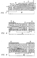
- FIGS 7-9 there are shown three alternate embodiments for various capacitor structures.
- the structures of Figures 8 and 9 can be used for capacitors which are substantially planar as shown, or for capacitors with high aspect ratios, wherein the sides of the electrodes contribute substantially to the total surface area of the electrodes in contact with the HDC material.
- FIG. 7 there is illustrated a high-dielectric-constant capacitor utilizing a lower electrode comprising a barrier layer.
- the barrier layer 34 is not used for direct electrical connection since electrical contact is made directly to Pt layer 36 from above, via a conductive TiN plug 46.
- the TiN plug 46 makes electrical contact to the aluminum top metallization 48 through the second SiO2 insulating layer 44.
- the two other TiN plugs 46 make electrical contact from the aluminum top metallization layer 48 to the Pt upper electrode 40 and to the doped silicon region 42.
- the lower electrode in Figure 7 is generally suitable only for low density devices since there is no direct path from the lower electrode to the substrate. Therefore, in this embodiment, barrier layer 34 does not need to be conductive after deposition of BST layer 38.
- Barrier layer 34 does need to remain conductive in Figures 8-9. Also, in these figures barrier layer 34 is directly exposed to the oxidizing conditions present during the deposition of BST layer 38 on the sides not covered by the oxygen stable layer. Many materials such as TiN oxidize rapidly under direct exposure to the HDC material deposition process. To alleviate this problem, Pt layer 36 could be formed on the sides of barrier layer 34 as well as on the top.
- barrier layer 34 provides electrical connection to and diffusion protection for oxidizable doped silicon region 42.
- barrier layer 34 provides electrical connection to and diffusion protection for oxidizable TiN/TiSi2/poly-silicon plug 50.
- 10nm of Ti is sputter deposited on poly-Si followed by an N2 rapid thermal anneal (700°C for 30 seconds) or NH3 furnace anneal (575°C for 10 minutes) to form a TiN/TiSi2/poly-Si structure. Excess TiN is then selectively removed chemically using peroxide.
- a vapor HF clean of a poly-Si layer is performed immediately prior to the deposition of a TiN layer, without using a TiSi2 layer. It is beneficial that the structure not be exposed to a contaminating environment, such as the atmosphere, between the HF clean and the adhesion layer deposition process steps, in order to ensure good adhesion between the poly-Si and the TiN layer.
- barrier layer 34 in Figure 9 could extend down into SiO2 layer 32 to form the plug itself or a portion thereof.
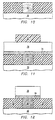
- FIG. 10-15 there is shown a method of forming another embodiment of this invention, an HDC material capacitor comprising a lower electrode with novel barrier materials.
- Figures 10-15 more clearly illustrate the effects of pre-oxidizing and annealing of the structure prior to the HDC material deposition.
- Figure 10 illustrates a silicon semiconductor substrate 30, with an SiO2 insulating layer 32 formed thereon.
- a TiN plug 50 has been formed in SiO2 layer 32.
- Figure 11 illustrates an unpatterned barrier layer 34 deposited on the SiO2 layer 32 directly over the TiN plug 52.
- An unpatterned Pt layer 36 is deposited on barrier layer 34.
- Figure 11 illustrates a layer of photoresist 52 that has been deposited and patterned on Pt layer 36 to form a mask for etching Pt layer 36 and barrier layer 34.
- Figure 12 illustrates the structure alter Pt layer 36 and barrier layer 34 have been etched, and photoresist 52 has been removed.
- Figure 13 illustrates the structure after partial pre-oxidation has formed oxidized sidewall 54 of barrier layer 34. Note that some barrier layer materials such as Pd-Si-O are already oxidized and will not form pre-oxidized sidewall 54. In the anneal process Pt layer 36 has rearranged to further round any corners after being etching. Sharp corners can cause excess leakage current, or possibly cracking in the BST layer 38.
- barrier layer materials such as Pd-Si-O are already oxidized and will not form pre-oxidized sidewall 54.
- Pt layer 36 has rearranged to further round any corners after being etching. Sharp corners can cause excess leakage current, or possibly cracking in the BST layer 38.
- BST layer 38 is deposited by MOCVD techniques on Pt layer 36 to form the structure shown in Figure 14.
- the deposition of BST layer 38 generally requires very oxidizing conditions, however Pt layer 36 will remain unoxidized, and barrier layer 34 will substantially inhibit oxygen from diffusing down to underlying materials.
- Figure 14 illustrates Pt upper electrode 40 deposited on BST layer 38 to form an HDC material capacitor structure.
- an oxygen stable Pt sidewall 56 has been formed using isotropic deposition and anisotropic etching. Pt sidewall 56 helps to protects barrier layer 34 from direct exposure to oxygen during BST deposition.
- barrier layer 34 is completely surrounded laterally by SiO2 layer 32, and completely covered by Pt layer 36. This structure effectively shields barrier layer 34 from direct exposure to oxygen during BST deposition without the extra process steps required to form the Pt sidewall 56 of Figure 16.
- rare earth nitrides are defined to be nitrides of the following elements: La, Ce, Pr, Nd, Pm, Sm, Eu, Gd, Tb, Dy, Ho, Er, Tm, Yb and Lu.
- processes for depositing the lower electrode materials include sputtering, reactive sputtering, sputtering as described with and without collimation and other enhancements, evaporation, and chemical or metalorganic chemical vapor deposition.
- processes for depositing the high-dielectric-constant material are sputtering, reactive sputtering with a metallic or oxide target, ion-beam sputtering, chemical vapor deposition, metalorganic chemical vapor deposition (with or without ions, electrons photons or plasma enhancement), sol-gel deposition, metalorganic decomposition and pulsed laser deposition.
- Layers that are described as alloys, compounds, mixtures, etc., are meant to be intentionally formed and substantial layers, as opposed to an unintentional partial mixture of the components of two separate layers that may be incidentally formed at the interface of those layers.
- the new barrier materials in general refer to nitrides. Actually, it is generally very difficult to deposit pure nitrides. There are almost always C and O "impurities" present. These impurities are frequently essential in order for the nitride to perform its function. For example, O in TiN is known to dramatically improve the barrier properties. Therefore, the novel barrier materials will also be assumed to have C and O impurities which might improve the properties even though they are not explicitly written in their formula. These C and O impurities might even be deliberately added. The sum of C and O will be less than 30 atom% with the rest N plus the required cations. For some applications, these impurities are probably required and in that case the sum of C and O will be more than 5 atom%.
Landscapes
- Semiconductor Memories (AREA)
- Electrodes Of Semiconductors (AREA)
- Semiconductor Integrated Circuits (AREA)
Applications Claiming Priority (2)
| Application Number | Priority Date | Filing Date | Title |
|---|---|---|---|
| US283873 | 1994-08-01 | ||
| US08/283,873 US5504041A (en) | 1994-08-01 | 1994-08-01 | Conductive exotic-nitride barrier layer for high-dielectric-constant materials |
Publications (2)
| Publication Number | Publication Date |
|---|---|
| EP0697719A2 true EP0697719A2 (de) | 1996-02-21 |
| EP0697719A3 EP0697719A3 (de) | 1997-12-03 |
Family
ID=23087933
Family Applications (1)
| Application Number | Title | Priority Date | Filing Date |
|---|---|---|---|
| EP95111973A Ceased EP0697719A3 (de) | 1994-08-01 | 1995-07-28 | Mikroelektronische Struktur mit einer Sperrschicht aus leitendem exotischen Nitrid für Elektroden mit einer hohen Dielektrizitätskonstante und Verfahren zu deren Herstellung |
Country Status (5)
| Country | Link |
|---|---|
| US (3) | US5504041A (de) |
| EP (1) | EP0697719A3 (de) |
| JP (1) | JPH0864786A (de) |
| KR (1) | KR960009156A (de) |
| TW (1) | TW284912B (de) |
Cited By (16)
| Publication number | Priority date | Publication date | Assignee | Title |
|---|---|---|---|---|
| DE19640448C1 (de) * | 1996-09-30 | 1998-02-19 | Siemens Ag | Verfahren zum Herstellen einer Halbleiteranordnung mit einem Kondensator |
| DE19640244A1 (de) * | 1996-09-30 | 1998-04-02 | Siemens Ag | Kondensator mit einem Elektrodenkern und einer dünnen Edelmetallschicht als erster Elektrode |
| DE19640246A1 (de) * | 1996-09-30 | 1998-04-02 | Siemens Ag | Halbleiteranordnung mit geschützter Barriere für eine Stapelzelle |
| EP0739030A3 (de) * | 1995-04-19 | 1998-07-08 | Nec Corporation | Hochintegrierter Dünnschichtkondensator mit einer Schicht hoher Dielektrizitätskonstante |
| DE19712540C1 (de) * | 1997-03-25 | 1998-08-13 | Siemens Ag | Herstellverfahren für eine Kondensatorelektrode aus einem Platinmetall |
| EP0926717A2 (de) | 1997-12-19 | 1999-06-30 | Siemens Aktiengesellschaft | Kondensatorelektrode aus Polysilizium |
| WO1999048154A1 (de) * | 1998-03-13 | 1999-09-23 | Siemens Aktiengesellschaft | Kondensator in integrierter schaltung |
| WO2000007246A1 (en) * | 1998-07-28 | 2000-02-10 | Applied Materials, Inc. | Method and apparatus for superior step coverage and interface control for high k dielectric capacitors and related electrodes |
| US6043529A (en) * | 1996-09-30 | 2000-03-28 | Siemens Aktiengesellschaft | Semiconductor configuration with a protected barrier for a stacked cell |
| EP1006590A1 (de) * | 1998-12-01 | 2000-06-07 | Rohm Co., Ltd. | Ferroelektrischer Speicher und Verfahren zur Herstellung |
| EP0955679A3 (de) * | 1998-05-08 | 2002-01-16 | Siemens Aktiengesellschaft | Stapelkondensateur mit verbesserter Stöpsel-Leitfähigkeit |
| WO2001059850A3 (en) * | 2000-02-08 | 2002-03-07 | Micron Technology Inc | Structures and methods for improved capacitor cells |
| EP0697720B1 (de) * | 1994-08-01 | 2003-01-15 | Texas Instruments Incorporated | Leitfähige Barriereschicht aus einem amorphen Nitrid als Elektrode für Material mit hoher dielektrischen Konstante |
| EP0967651A3 (de) * | 1998-06-24 | 2003-11-19 | Matsushita Electric Industrial Co., Ltd. | Halbleiterspeicher mit Kondensatordielektrikum |
| DE102004022604A1 (de) * | 2004-05-07 | 2005-12-08 | Infineon Technologies Ag | Verfahren zur Herstellung einer sublithographischen Kontaktstruktur in einem Halbleiterbauelement |
| US12426506B2 (en) | 2019-07-19 | 2025-09-23 | Evatec Ag | Piezoelectric coating and deposition process |
Families Citing this family (218)
| Publication number | Priority date | Publication date | Assignee | Title |
|---|---|---|---|---|
| DE69404189T2 (de) * | 1993-03-31 | 1998-01-08 | Texas Instruments Inc | Leicht donatoren-dotierte Elektroden für Materialien mit hoher dielektrischer Konstante |
| US5499207A (en) * | 1993-08-06 | 1996-03-12 | Hitachi, Ltd. | Semiconductor memory device having improved isolation between electrodes, and process for fabricating the same |
| US6404003B1 (en) | 1999-07-28 | 2002-06-11 | Symetrix Corporation | Thin film capacitors on silicon germanium substrate |
| US6639262B2 (en) | 1993-12-10 | 2003-10-28 | Symetrix Corporation | Metal oxide integrated circuit on silicon germanium substrate |
| US6770924B1 (en) | 1994-05-13 | 2004-08-03 | Micron Technology, Inc. | Amorphous TiN films for an integrated capacitor dielectric/bottom plate using high dielectric constant materials |
| US6107105A (en) * | 1994-05-13 | 2000-08-22 | Micron Technology, Inc. | Amorphous tin films for an integrated capacitor dielectric/bottom plate using high dielectric constant material |
| US5622893A (en) * | 1994-08-01 | 1997-04-22 | Texas Instruments Incorporated | Method of forming conductive noble-metal-insulator-alloy barrier layer for high-dielectric-constant material electrodes |
| US5965942A (en) * | 1994-09-28 | 1999-10-12 | Sharp Kabushiki Kaisha | Semiconductor memory device with amorphous diffusion barrier between capacitor and plug |
| KR100342296B1 (ko) * | 1994-10-04 | 2002-11-29 | 코닌클리케 필립스 일렉트로닉스 엔.브이. | 산소장벽이마련된하부전극을가지는강유전성의메모리소자를포함하는반도체장치와그의제조방법 |
| US5563762A (en) * | 1994-11-28 | 1996-10-08 | Northern Telecom Limited | Capacitor for an integrated circuit and method of formation thereof, and a method of adding on-chip capacitors to an integrated circuit |
| US5576579A (en) * | 1995-01-12 | 1996-11-19 | International Business Machines Corporation | Tasin oxygen diffusion barrier in multilayer structures |
| US5614437A (en) * | 1995-01-26 | 1997-03-25 | Lsi Logic Corporation | Method for fabricating reliable metallization with Ta-Si-N barrier for semiconductors |
| US5874364A (en) * | 1995-03-27 | 1999-02-23 | Fujitsu Limited | Thin film deposition method, capacitor device and method for fabricating the same, and semiconductor device and method for fabricating the same |
| KR100199346B1 (ko) * | 1995-04-04 | 1999-06-15 | 김영환 | 반도체 소자의 전하저장전극 형성방법 |
| US5665625A (en) * | 1995-05-19 | 1997-09-09 | Micron Technology, Inc. | Method of forming capacitors having an amorphous electrically conductive layer |
| US5663088A (en) * | 1995-05-19 | 1997-09-02 | Micron Technology, Inc. | Method of forming a Ta2 O5 dielectric layer with amorphous diffusion barrier layer and method of forming a capacitor having a Ta2 O5 dielectric layer and amorphous diffusion barrier layer |
| US5629229A (en) * | 1995-07-12 | 1997-05-13 | Sharp Kabushiki Kaisha | Metalorganic chemical vapor deposition of (Ba1-x Srx)RuO3 /(Ba1-x Srx)TIO3 /(Ba1-x Srx)TiO3 /(Ba1- Srx)RuO3 capacitors for high dielectric materials |
| US5786248A (en) * | 1995-10-12 | 1998-07-28 | Micron Technology, Inc. | Semiconductor processing method of forming a tantalum oxide containing capacitor |
| JPH09191088A (ja) | 1995-11-09 | 1997-07-22 | Mitsubishi Electric Corp | 半導体記憶装置およびその製造方法 |
| US6432767B2 (en) | 1995-12-05 | 2002-08-13 | Hitachi, Ltd. | Method of fabricating semiconductor device |
| JP3504046B2 (ja) * | 1995-12-05 | 2004-03-08 | 株式会社ルネサステクノロジ | 半導体装置の製造方法 |
| US5716875A (en) * | 1996-03-01 | 1998-02-10 | Motorola, Inc. | Method for making a ferroelectric device |
| KR100215867B1 (ko) * | 1996-04-12 | 1999-08-16 | 구본준 | 반도체 소자의 커패시터 구조 및 제조 방법 |
| US6239492B1 (en) * | 1996-05-08 | 2001-05-29 | Micron Technology, Inc. | Semiconductor structure with a titanium aluminum nitride layer and method for fabricating same |
| TW373320B (en) * | 1996-05-27 | 1999-11-01 | United Microelectronics Corporaiton | Structure and production method of capacitor of dynamic RAM |
| US5892281A (en) | 1996-06-10 | 1999-04-06 | Micron Technology, Inc. | Tantalum-aluminum-nitrogen material for semiconductor devices |
| US5843830A (en) * | 1996-06-26 | 1998-12-01 | Micron Technology, Inc. | Capacitor, and methods for forming a capacitor |
| DE19630883A1 (de) * | 1996-07-31 | 1998-02-05 | Philips Patentverwaltung | Bauteil mit einem Kondensator |
| WO1998006131A1 (fr) * | 1996-08-07 | 1998-02-12 | Hitachi, Ltd. | Composant a semi-conducteur et son procede de fabrication |
| US6251720B1 (en) | 1996-09-27 | 2001-06-26 | Randhir P. S. Thakur | High pressure reoxidation/anneal of high dielectric constant materials |
| DE19646208C2 (de) * | 1996-11-08 | 2001-08-30 | Infineon Technologies Ag | Verfahren zur Herstellung eines Kondensators und Speicherfeld |
| KR100190111B1 (ko) * | 1996-11-13 | 1999-06-01 | 윤종용 | 반도체장치의 커패시터 제조방법 |
| US6130124A (en) * | 1996-12-04 | 2000-10-10 | Samsung Electronics Co., Ltd. | Methods of forming capacitor electrodes having reduced susceptibility to oxidation |
| US5932907A (en) * | 1996-12-24 | 1999-08-03 | International Business Machines Corporation | Method, materials, and structures for noble metal electrode contacts to silicon |
| KR100400290B1 (ko) * | 1996-12-31 | 2003-12-24 | 주식회사 하이닉스반도체 | 반도체 소자의 캐패시터 제조방법 |
| KR19980060522A (ko) * | 1996-12-31 | 1998-10-07 | 김영환 | 반도체 소자의 캐패시터 제조방법 |
| KR100227843B1 (ko) * | 1997-01-22 | 1999-11-01 | 윤종용 | 반도체 소자의 콘택 배선 방법 및 이를 이용한 커패시터 제조방법 |
| KR100243285B1 (ko) * | 1997-02-27 | 2000-02-01 | 윤종용 | 고유전 커패시터 및 그 제조방법 |
| US5744387A (en) * | 1997-03-07 | 1998-04-28 | Vanguard International Semiconductor Corporation | Method for fabricating dynamic random access memory with a flat topography and fewer photomasks |
| US5998257A (en) | 1997-03-13 | 1999-12-07 | Micron Technology, Inc. | Semiconductor processing methods of forming integrated circuitry memory devices, methods of forming capacitor containers, methods of making electrical connection to circuit nodes and related integrated circuitry |
| KR100258599B1 (ko) * | 1997-03-14 | 2000-06-15 | 윤종용 | 강유전체메모리셀의제조방법 |
| KR100230418B1 (ko) * | 1997-04-17 | 1999-11-15 | 윤종용 | 백금족 금속층 형성방법 및 이를 이용한 커패시터 제조방법 |
| US6849557B1 (en) | 1997-04-30 | 2005-02-01 | Micron Technology, Inc. | Undoped silicon dioxide as etch stop for selective etch of doped silicon dioxide |
| KR100273988B1 (ko) * | 1997-04-30 | 2001-01-15 | 윤종용 | 커패시터제조방법(Method For Making a Capacitor) |
| US6335238B1 (en) * | 1997-05-08 | 2002-01-01 | Texas Instruments Incorporated | Integrated dielectric and method |
| US5796573A (en) * | 1997-05-29 | 1998-08-18 | International Business Machines Corporation | Overhanging separator for self-defining stacked capacitor |
| US6153491A (en) * | 1997-05-29 | 2000-11-28 | International Business Machines Corporation | Overhanging separator for self-defining discontinuous film |
| US6002575A (en) * | 1997-05-29 | 1999-12-14 | International Business Machines Corporation | Adherent separator for self-defining discontinuous film |
| US5955756A (en) * | 1997-05-29 | 1999-09-21 | International Business Machines Corporation | Trench separator for self-defining discontinuous film |
| JP3452800B2 (ja) * | 1997-06-30 | 2003-09-29 | ヒュンダイ エレクトロニクス インダストリーズ カムパニー リミテッド | 高集積記憶素子およびその製造方法 |
| US6090697A (en) * | 1997-06-30 | 2000-07-18 | Texas Instruments Incorporated | Etchstop for integrated circuits |
| US6600183B1 (en) | 1997-07-01 | 2003-07-29 | Texas Instruments Incorporated | Integrated circuit capacitor and memory |
| US6153490A (en) * | 1997-07-01 | 2000-11-28 | Texas Instruments Incorporated | Method for forming integrated circuit capacitor and memory |
| US7115461B2 (en) * | 1997-07-24 | 2006-10-03 | Texas Instruments Incorporated | High permittivity silicate gate dielectric |
| US6013553A (en) | 1997-07-24 | 2000-01-11 | Texas Instruments Incorporated | Zirconium and/or hafnium oxynitride gate dielectric |
| US6841439B1 (en) * | 1997-07-24 | 2005-01-11 | Texas Instruments Incorporated | High permittivity silicate gate dielectric |
| US5910880A (en) * | 1997-08-20 | 1999-06-08 | Micron Technology, Inc. | Semiconductor circuit components and capacitors |
| US6204525B1 (en) * | 1997-09-22 | 2001-03-20 | Murata Manufacturing Co., Ltd. | Ferroelectric thin film device and method of producing the same |
| KR100269310B1 (ko) * | 1997-09-29 | 2000-10-16 | 윤종용 | 도전성확산장벽층을사용하는반도체장치제조방법 |
| JP3878724B2 (ja) * | 1997-10-14 | 2007-02-07 | 株式会社ルネサステクノロジ | 半導体集積回路装置およびその製造方法 |
| US6074885A (en) * | 1997-11-25 | 2000-06-13 | Radiant Technologies, Inc | Lead titanate isolation layers for use in fabricating PZT-based capacitors and similar structures |
| KR100280206B1 (ko) * | 1997-12-06 | 2001-03-02 | 윤종용 | 고유전체 캐패시터 및 그의 제조 방법 |
| US6165833A (en) * | 1997-12-19 | 2000-12-26 | Micron Technology, Inc. | Semiconductor processing method of forming a capacitor |
| US6320213B1 (en) | 1997-12-19 | 2001-11-20 | Advanced Technology Materials, Inc. | Diffusion barriers between noble metal electrodes and metallization layers, and integrated circuit and semiconductor devices comprising same |
| US6911371B2 (en) | 1997-12-19 | 2005-06-28 | Micron Technology, Inc. | Capacitor forming methods with barrier layers to threshold voltage shift inducing material |
| US6285050B1 (en) * | 1997-12-24 | 2001-09-04 | International Business Machines Corporation | Decoupling capacitor structure distributed above an integrated circuit and method for making same |
| KR100252854B1 (ko) * | 1997-12-26 | 2000-04-15 | 김영환 | 반도체 메모리 장치 및 그 제조방법 |
| KR100436058B1 (ko) | 1997-12-27 | 2004-12-17 | 주식회사 하이닉스반도체 | 강유전체 캐패시터 형성 방법 |
| US6303952B1 (en) * | 1998-01-14 | 2001-10-16 | Texas Instruments Incorporated | Contact structure with an oxide silicidation barrier |
| JP3211950B2 (ja) * | 1998-01-19 | 2001-09-25 | 日本電気株式会社 | 半導体装置およびその製造方法 |
| US6178082B1 (en) * | 1998-02-26 | 2001-01-23 | International Business Machines Corporation | High temperature, conductive thin film diffusion barrier for ceramic/metal systems |
| US6162744A (en) * | 1998-02-28 | 2000-12-19 | Micron Technology, Inc. | Method of forming capacitors having high-K oxygen containing capacitor dielectric layers, method of processing high-K oxygen containing dielectric layers, method of forming a DRAM cell having having high-K oxygen containing capacitor dielectric layers |
| US6191443B1 (en) | 1998-02-28 | 2001-02-20 | Micron Technology, Inc. | Capacitors, methods of forming capacitors, and DRAM memory cells |
| US6111285A (en) * | 1998-03-17 | 2000-08-29 | Micron Technology, Inc. | Boride electrodes and barriers for cell dielectrics |
| US6156638A (en) | 1998-04-10 | 2000-12-05 | Micron Technology, Inc. | Integrated circuitry and method of restricting diffusion from one material to another |
| US6730559B2 (en) | 1998-04-10 | 2004-05-04 | Micron Technology, Inc. | Capacitors and methods of forming capacitors |
| US6165834A (en) * | 1998-05-07 | 2000-12-26 | Micron Technology, Inc. | Method of forming capacitors, method of processing dielectric layers, method of forming a DRAM cell |
| US6255186B1 (en) | 1998-05-21 | 2001-07-03 | Micron Technology, Inc. | Methods of forming integrated circuitry and capacitors having a capacitor electrode having a base and a pair of walls projecting upwardly therefrom |
| KR100292689B1 (ko) * | 1998-06-03 | 2001-07-12 | 김영환 | 캐패시터및그형성방법 |
| KR100318453B1 (ko) * | 1998-06-29 | 2002-03-08 | 박종섭 | 이리듐막및백금막의이중막구조의하부전극을갖는캐패시터형성방법 |
| KR100301371B1 (ko) * | 1998-07-03 | 2001-10-27 | 윤종용 | 반도체메모리장치및그의제조방법 |
| US6277758B1 (en) | 1998-07-23 | 2001-08-21 | Micron Technology, Inc. | Method of etching doped silicon dioxide with selectivity to undoped silicon dioxide with a high density plasma etcher |
| US6197628B1 (en) * | 1998-08-27 | 2001-03-06 | Micron Technology, Inc. | Ruthenium silicide diffusion barrier layers and methods of forming same |
| US6184550B1 (en) | 1998-08-28 | 2001-02-06 | Advanced Technology Materials, Inc. | Ternary nitride-carbide barrier layers |
| US6204172B1 (en) | 1998-09-03 | 2001-03-20 | Micron Technology, Inc. | Low temperature deposition of barrier layers |
| US6323081B1 (en) | 1998-09-03 | 2001-11-27 | Micron Technology, Inc. | Diffusion barrier layers and methods of forming same |
| US6780758B1 (en) * | 1998-09-03 | 2004-08-24 | Micron Technology, Inc. | Method of establishing electrical contact between a semiconductor substrate and a semiconductor device |
| US6136660A (en) * | 1998-09-28 | 2000-10-24 | Siemens Aktiengesellschaft | Stacked capacitator memory cell and method of fabrication |
| KR100293720B1 (ko) * | 1998-10-01 | 2001-07-12 | 박종섭 | 반도체 소자의 캐패시터 형성 방법 |
| TW386286B (en) * | 1998-10-26 | 2000-04-01 | Ind Tech Res Inst | An ohmic contact of semiconductor and the manufacturing method |
| DE19849542C2 (de) * | 1998-10-27 | 2002-07-11 | Infineon Technologies Ag | Verfahren zur Herstellung eines Kondensators |
| KR100318457B1 (ko) * | 1998-10-28 | 2002-02-19 | 박종섭 | 플라즈마를이용한강유전체박막형성방법 |
| US6433993B1 (en) * | 1998-11-23 | 2002-08-13 | Microcoating Technologies, Inc. | Formation of thin film capacitors |
| KR100324591B1 (ko) * | 1998-12-24 | 2002-04-17 | 박종섭 | 티타늄 알루미늄 질소 합금막을 상부전극의 확산방지막으로서 이용하는 캐패시터 제조 방법 |
| KR100504430B1 (ko) * | 1998-12-30 | 2006-05-17 | 주식회사 하이닉스반도체 | 플러그를갖는커패시터의하부전극형성방법 |
| US6075264A (en) | 1999-01-25 | 2000-06-13 | Samsung Electronics Co., Ltd. | Structure of a ferroelectric memory cell and method of fabricating it |
| US6495409B1 (en) | 1999-01-26 | 2002-12-17 | Agere Systems Inc. | MOS transistor having aluminum nitride gate structure and method of manufacturing same |
| US6387748B1 (en) | 1999-02-16 | 2002-05-14 | Micron Technology, Inc. | Semiconductor circuit constructions, capacitor constructions, and methods of forming semiconductor circuit constructions and capacitor constructions |
| US6291363B1 (en) | 1999-03-01 | 2001-09-18 | Micron Technology, Inc. | Surface treatment of DARC films to reduce defects in subsequent cap layers |
| US6445023B1 (en) * | 1999-03-16 | 2002-09-03 | Micron Technology, Inc. | Mixed metal nitride and boride barrier layers |
| US6723436B1 (en) * | 1999-03-22 | 2004-04-20 | California Institute Of Technology | Electrically conducting ternary amorphous fully oxidized materials and their application |
| KR100287187B1 (ko) * | 1999-03-30 | 2001-04-16 | 윤종용 | 반도체소자의 커패시터 및 그 제조방법 |
| US6268260B1 (en) * | 1999-03-31 | 2001-07-31 | Lam Research Corporation | Methods of forming memory cell capacitor plates in memory cell capacitor structures |
| JP2004343150A (ja) * | 1999-06-02 | 2004-12-02 | Matsushita Electric Ind Co Ltd | 半導体装置の製造方法 |
| JP2001015696A (ja) * | 1999-06-29 | 2001-01-19 | Nec Corp | 水素バリヤ層及び半導体装置 |
| US6339258B1 (en) | 1999-07-02 | 2002-01-15 | International Business Machines Corporation | Low resistivity tantalum |
| US6465828B2 (en) | 1999-07-30 | 2002-10-15 | Micron Technology, Inc. | Semiconductor container structure with diffusion barrier |
| KR100358063B1 (ko) * | 1999-08-04 | 2002-10-25 | 주식회사 하이닉스반도체 | 반도체 소자의 캐패시터 제조 방법 |
| US6197651B1 (en) | 1999-08-30 | 2001-03-06 | Taiwan Semiconductor Manufacturing Company | Structure and method for forming a capacitor dielectric using yttrium barium copper oxide |
| US6281543B1 (en) | 1999-08-31 | 2001-08-28 | Micron Technology, Inc. | Double layer electrode and barrier system on hemispherical grain silicon for use with high dielectric constant materials and methods for fabricating the same |
| TW432689B (en) * | 1999-10-18 | 2001-05-01 | Taiwan Semiconductor Mfg | Fabricating method of stacked capacitor |
| US7071520B2 (en) | 2000-08-23 | 2006-07-04 | Reflectivity, Inc | MEMS with flexible portions made of novel materials |
| US6720096B1 (en) | 1999-11-17 | 2004-04-13 | Sanyo Electric Co., Ltd. | Dielectric element |
| DE19958203A1 (de) * | 1999-12-02 | 2001-06-13 | Infineon Technologies Ag | Herstellungsverfahren einer oxidationsgeschüzten Elektrode für einen kapazitive Elektrodenstruktur |
| US6780704B1 (en) * | 1999-12-03 | 2004-08-24 | Asm International Nv | Conformal thin films over textured capacitor electrodes |
| DE19959711A1 (de) | 1999-12-10 | 2001-06-21 | Infineon Technologies Ag | Verfahren zur Herstellung einer strukturierten Metallschicht |
| US6635528B2 (en) * | 1999-12-22 | 2003-10-21 | Texas Instruments Incorporated | Method of planarizing a conductive plug situated under a ferroelectric capacitor |
| KR100376264B1 (ko) | 1999-12-24 | 2003-03-17 | 주식회사 하이닉스반도체 | 게이트 유전체막이 적용되는 반도체 소자의 제조 방법 |
| US6801422B2 (en) * | 1999-12-28 | 2004-10-05 | Intel Corporation | High performance capacitor |
| US6475854B2 (en) | 1999-12-30 | 2002-11-05 | Applied Materials, Inc. | Method of forming metal electrodes |
| KR100351451B1 (ko) * | 1999-12-30 | 2002-09-09 | 주식회사 하이닉스반도체 | 반도체메모리장치의 커패시터제조방법 |
| DE10000005C1 (de) * | 2000-01-03 | 2001-09-13 | Infineon Technologies Ag | Verfahren zur Herstellung eines ferroelektrischen Halbleiterspeichers |
| US20020197793A1 (en) * | 2000-01-06 | 2002-12-26 | Dornfest Charles N | Low thermal budget metal oxide deposition for capacitor structures |
| US6417537B1 (en) * | 2000-01-18 | 2002-07-09 | Micron Technology, Inc. | Metal oxynitride capacitor barrier layer |
| US6461973B1 (en) * | 2000-02-11 | 2002-10-08 | Advanced Micro Devices, Inc. | Method for forming high quality multiple thickness oxide layers by reducing descum induced defects |
| JP2001237395A (ja) * | 2000-02-22 | 2001-08-31 | Matsushita Electric Ind Co Ltd | 半導体記憶装置 |
| US7005695B1 (en) * | 2000-02-23 | 2006-02-28 | Micron Technology, Inc. | Integrated circuitry including a capacitor with an amorphous and a crystalline high K capacitor dielectric region |
| JP2001267529A (ja) * | 2000-03-22 | 2001-09-28 | Tokyo Electron Ltd | 半導体装置およびその製造方法 |
| US6724611B1 (en) * | 2000-03-29 | 2004-04-20 | Intel Corporation | Multi-layer chip capacitor |
| US6492241B1 (en) | 2000-04-10 | 2002-12-10 | Micron Technology, Inc. | Integrated capacitors fabricated with conductive metal oxides |
| US6417062B1 (en) * | 2000-05-01 | 2002-07-09 | General Electric Company | Method of forming ruthenium oxide films |
| US6528180B1 (en) | 2000-05-23 | 2003-03-04 | Applied Materials, Inc. | Liner materials |
| US6579783B2 (en) | 2000-07-07 | 2003-06-17 | Applied Materials, Inc. | Method for high temperature metal deposition for reducing lateral silicidation |
| US6352921B1 (en) | 2000-07-19 | 2002-03-05 | Chartered Semiconductor Manufacturing Ltd. | Use of boron carbide as an etch-stop and barrier layer for copper dual damascene metallization |
| US6423632B1 (en) | 2000-07-21 | 2002-07-23 | Motorola, Inc. | Semiconductor device and a process for forming the same |
| US6627050B2 (en) | 2000-07-28 | 2003-09-30 | Applied Materials, Inc. | Method and apparatus for depositing a tantalum-containing layer on a substrate |
| US6517944B1 (en) | 2000-08-03 | 2003-02-11 | Teracomm Research Inc. | Multi-layer passivation barrier for a superconducting element |
| US7057246B2 (en) | 2000-08-23 | 2006-06-06 | Reflectivity, Inc | Transition metal dielectric alloy materials for MEMS |
| US7153592B2 (en) * | 2000-08-31 | 2006-12-26 | Fujitsu Limited | Organic EL element and method of manufacturing the same, organic EL display device using the element, organic EL material, and surface emission device and liquid crystal display device using the material |
| US6430448B1 (en) | 2000-11-07 | 2002-08-06 | Pacesetter, Inc. | Stimulating electrode having low polarization and method of making same |
| US6430447B1 (en) | 2000-11-07 | 2002-08-06 | Pacesetter, Inc. | Stimulating electrode having low polarization and method of making same |
| JP2002151657A (ja) | 2000-11-08 | 2002-05-24 | Sanyo Electric Co Ltd | 誘電体素子およびその製造方法 |
| KR20020049875A (ko) * | 2000-12-20 | 2002-06-26 | 윤종용 | 반도체 메모리 소자의 강유전체 커패시터 및 그 제조방법 |
| US7378719B2 (en) | 2000-12-20 | 2008-05-27 | Micron Technology, Inc. | Low leakage MIM capacitor |
| KR100390834B1 (ko) * | 2000-12-26 | 2003-07-10 | 주식회사 하이닉스반도체 | 반도체 소자 및 그 제조 방법 |
| US6524867B2 (en) | 2000-12-28 | 2003-02-25 | Micron Technology, Inc. | Method for forming platinum-rhodium stack as an oxygen barrier |
| KR100387262B1 (ko) * | 2000-12-29 | 2003-06-12 | 주식회사 하이닉스반도체 | 반도체 소자의 캐패시터 제조 방법 |
| JP2002231903A (ja) * | 2001-02-06 | 2002-08-16 | Sanyo Electric Co Ltd | 誘電体素子およびその製造方法 |
| US6518610B2 (en) | 2001-02-20 | 2003-02-11 | Micron Technology, Inc. | Rhodium-rich oxygen barriers |
| US6563161B2 (en) | 2001-03-22 | 2003-05-13 | Winbond Electronics Corporation | Memory-storage node and the method of fabricating the same |
| KR100406536B1 (ko) | 2001-03-28 | 2003-11-20 | 주식회사 하이닉스반도체 | 산소확산방지막으로서 알루미늄 산화막을 구비하는강유전체 메모리 소자 및 그 제조 방법 |
| US6688584B2 (en) * | 2001-05-16 | 2004-02-10 | Micron Technology, Inc. | Compound structure for reduced contact resistance |
| KR100418581B1 (ko) * | 2001-06-12 | 2004-02-11 | 주식회사 하이닉스반도체 | 메모리 소자의 제조방법 |
| US7057251B2 (en) * | 2001-07-20 | 2006-06-06 | Reflectivity, Inc | MEMS device made of transition metal-dielectric oxide materials |
| US8110489B2 (en) | 2001-07-25 | 2012-02-07 | Applied Materials, Inc. | Process for forming cobalt-containing materials |
| US20090004850A1 (en) | 2001-07-25 | 2009-01-01 | Seshadri Ganguli | Process for forming cobalt and cobalt silicide materials in tungsten contact applications |
| US20030029715A1 (en) | 2001-07-25 | 2003-02-13 | Applied Materials, Inc. | An Apparatus For Annealing Substrates In Physical Vapor Deposition Systems |
| US9051641B2 (en) | 2001-07-25 | 2015-06-09 | Applied Materials, Inc. | Cobalt deposition on barrier surfaces |
| JP2005504885A (ja) | 2001-07-25 | 2005-02-17 | アプライド マテリアルズ インコーポレイテッド | 新規なスパッタ堆積方法を使用したバリア形成 |
| US7297626B1 (en) * | 2001-08-27 | 2007-11-20 | United States Of America As Represented By The Secretary Of The Army | Process for nickel silicide Ohmic contacts to n-SiC |
| US6989108B2 (en) * | 2001-08-30 | 2006-01-24 | Micron Technology, Inc. | Etchant gas composition |
| KR100442709B1 (ko) * | 2001-09-22 | 2004-08-02 | 학교법인 국민학원 | 이종 질화물의 이중 방지막을 갖는 커패시터 및 그의 전극형성 방법 |
| KR100424710B1 (ko) * | 2001-11-21 | 2004-03-27 | 주식회사 하이닉스반도체 | 반도체 소자의 제조방법 |
| KR100438781B1 (ko) * | 2001-12-05 | 2004-07-05 | 삼성전자주식회사 | 금속-절연체-금속 캐패시터 및 그 제조방법 |
| KR100447972B1 (ko) * | 2001-12-27 | 2004-09-10 | 주식회사 하이닉스반도체 | 반도체 소자의 캐패시터 형성방법 |
| US6972265B1 (en) * | 2002-04-15 | 2005-12-06 | Silicon Magnetic Systems | Metal etch process selective to metallic insulating materials |
| DE10218799A1 (de) * | 2002-04-23 | 2003-11-13 | Ihp Gmbh | Halbleiterkondensator mit Praseodymoxid als Dielektrikum |
| US6717266B1 (en) * | 2002-06-18 | 2004-04-06 | Advanced Micro Devices, Inc. | Use of an alloying element to form a stable oxide layer on the surface of metal features |
| US7067862B2 (en) * | 2002-08-02 | 2006-06-27 | Unity Semiconductor Corporation | Conductive memory device with conductive oxide electrodes |
| US8236443B2 (en) | 2002-08-09 | 2012-08-07 | Infinite Power Solutions, Inc. | Metal film encapsulation |
| US8445130B2 (en) | 2002-08-09 | 2013-05-21 | Infinite Power Solutions, Inc. | Hybrid thin-film battery |
| US8394522B2 (en) | 2002-08-09 | 2013-03-12 | Infinite Power Solutions, Inc. | Robust metal film encapsulation |
| US7993773B2 (en) | 2002-08-09 | 2011-08-09 | Infinite Power Solutions, Inc. | Electrochemical apparatus with barrier layer protected substrate |
| US8404376B2 (en) | 2002-08-09 | 2013-03-26 | Infinite Power Solutions, Inc. | Metal film encapsulation |
| US20070264564A1 (en) * | 2006-03-16 | 2007-11-15 | Infinite Power Solutions, Inc. | Thin film battery on an integrated circuit or circuit board and method thereof |
| US8431264B2 (en) | 2002-08-09 | 2013-04-30 | Infinite Power Solutions, Inc. | Hybrid thin-film battery |
| US8021778B2 (en) | 2002-08-09 | 2011-09-20 | Infinite Power Solutions, Inc. | Electrochemical apparatus with barrier layer protected substrate |
| JP4840794B2 (ja) * | 2002-08-30 | 2011-12-21 | 国立大学法人東京工業大学 | 電子デバイスの製造方法 |
| KR100480469B1 (ko) * | 2002-10-17 | 2005-04-07 | 동부아남반도체 주식회사 | 반도체 소자내 커패시터 제조방법 |
| US6794753B2 (en) * | 2002-12-27 | 2004-09-21 | Lexmark International, Inc. | Diffusion barrier and method therefor |
| US20040140296A1 (en) * | 2003-01-22 | 2004-07-22 | Lis Steven A. | Close proximity pulsed laser catalyst deposition system and method |
| US7042705B2 (en) * | 2003-01-30 | 2006-05-09 | Infineon Technologies Ag | Sidewall structure and method of fabrication for reducing oxygen diffusion to contact plugs during CW hole reactive ion etch processing |
| KR100536030B1 (ko) * | 2003-02-25 | 2005-12-12 | 삼성전자주식회사 | 반도체 장치의 커패시터 형성 방법 |
| JP2004281965A (ja) * | 2003-03-19 | 2004-10-07 | Matsushita Electric Ind Co Ltd | 半導体装置及びその製造方法 |
| US7531380B2 (en) * | 2003-04-30 | 2009-05-12 | Cree, Inc. | Methods of forming light-emitting devices having an active region with electrical contacts coupled to opposing surfaces thereof |
| US7123969B1 (en) | 2003-05-21 | 2006-10-17 | Pacesetter, Inc. | Lead having one or more low polarization electrodes |
| US8728285B2 (en) | 2003-05-23 | 2014-05-20 | Demaray, Llc | Transparent conductive oxides |
| US6849465B2 (en) * | 2003-06-20 | 2005-02-01 | Infineon Technologies Ag | Method of patterning a magnetic memory cell bottom electrode before magnetic stack deposition |
| US6849891B1 (en) * | 2003-12-08 | 2005-02-01 | Sharp Laboratories Of America, Inc. | RRAM memory cell electrodes |
| US7080896B2 (en) * | 2004-01-20 | 2006-07-25 | Lexmark International, Inc. | Micro-fluid ejection device having high resistance heater film |
| US7301752B2 (en) * | 2004-06-04 | 2007-11-27 | International Business Machines Corporation | Formation of metal-insulator-metal capacitor simultaneously with aluminum metal wiring level using a hardmask |
| US20060014624A1 (en) * | 2004-07-15 | 2006-01-19 | Biljana Mikijelj | High dielectric strength monolithic Si3N4 |
| KR101127370B1 (ko) | 2004-12-08 | 2012-03-29 | 인피니트 파워 솔루션스, 인크. | LiCoO2의 증착 |
| US7959769B2 (en) | 2004-12-08 | 2011-06-14 | Infinite Power Solutions, Inc. | Deposition of LiCoO2 |
| US7371684B2 (en) * | 2005-05-16 | 2008-05-13 | International Business Machines Corporation | Process for preparing electronics structures using a sacrificial multilayer hardmask scheme |
| JP2007053141A (ja) * | 2005-08-15 | 2007-03-01 | Fujitsu Ltd | 半導体装置およびその製造方法 |
| JP4703349B2 (ja) * | 2005-10-11 | 2011-06-15 | Okiセミコンダクタ株式会社 | アモルファス膜の成膜方法 |
| US7534693B2 (en) * | 2006-01-04 | 2009-05-19 | Freescale Semiconductor, Inc. | Thin-film capacitor with a field modification layer and methods for forming the same |
| JP4703500B2 (ja) * | 2006-06-30 | 2011-06-15 | 富士通セミコンダクター株式会社 | 半導体装置の製造方法 |
| CN101523571A (zh) | 2006-09-29 | 2009-09-02 | 无穷动力解决方案股份有限公司 | 柔性基板上沉积的电池层的掩模和材料限制 |
| TWI330741B (en) | 2006-11-02 | 2010-09-21 | Au Optronics Corp | Supporting structure and backlight module using the same |
| US8197781B2 (en) | 2006-11-07 | 2012-06-12 | Infinite Power Solutions, Inc. | Sputtering target of Li3PO4 and method for producing same |
| US7713866B2 (en) * | 2006-11-21 | 2010-05-11 | Infineon Technologies Ag | Semiconductor devices and methods of manufacture thereof |
| US20080293192A1 (en) * | 2007-05-22 | 2008-11-27 | Stefan Zollner | Semiconductor device with stressors and methods thereof |
| US20090108294A1 (en) * | 2007-10-30 | 2009-04-30 | International Business Machines Corporation | Scalable high-k dielectric gate stack |
| US8268488B2 (en) | 2007-12-21 | 2012-09-18 | Infinite Power Solutions, Inc. | Thin film electrolyte for thin film batteries |
| CN101903560B (zh) | 2007-12-21 | 2014-08-06 | 无穷动力解决方案股份有限公司 | 用于电解质膜的溅射靶的方法 |
| US8518581B2 (en) | 2008-01-11 | 2013-08-27 | Inifinite Power Solutions, Inc. | Thin film encapsulation for thin film batteries and other devices |
| JP5262233B2 (ja) * | 2008-03-27 | 2013-08-14 | 日本電気株式会社 | 窒化ジルコニウム界面層を有するキャパシター構造 |
| WO2009124191A2 (en) | 2008-04-02 | 2009-10-08 | Infinite Power Solutions, Inc. | Passive over/under voltage control and protection for energy storage devices associated with energy harvesting |
| JP2012500610A (ja) * | 2008-08-11 | 2012-01-05 | インフィニット パワー ソリューションズ, インコーポレイテッド | 電磁エネルギー獲得ための統合コレクタ表面を有するエネルギーデバイスおよびその方法 |
| CN102150185B (zh) | 2008-09-12 | 2014-05-28 | 无穷动力解决方案股份有限公司 | 具有经由电磁能进行数据通信的组成导电表面的能量装置及其方法 |
| WO2010042594A1 (en) | 2008-10-08 | 2010-04-15 | Infinite Power Solutions, Inc. | Environmentally-powered wireless sensor module |
| CN102576828B (zh) | 2009-09-01 | 2016-04-20 | 萨普拉斯特研究有限责任公司 | 具有集成薄膜电池的印刷电路板 |
| EP2577777B1 (de) | 2010-06-07 | 2016-12-28 | Sapurast Research LLC | Wiederaufladbare elektrochemische vorrichtung von hoher dichte |
| US9299926B2 (en) | 2012-02-17 | 2016-03-29 | Intermolecular, Inc. | Nonvolatile memory device using a tunnel oxide layer and oxygen blocking layer as a current limiter element |
| CN108257957A (zh) * | 2016-12-29 | 2018-07-06 | 联华电子股份有限公司 | 半导体结构及其制作方法 |
| US11133462B2 (en) | 2019-06-10 | 2021-09-28 | International Business Machines Corporation | Bottom electrode structure and method of forming the same |
Citations (5)
| Publication number | Priority date | Publication date | Assignee | Title |
|---|---|---|---|---|
| EP0404295A1 (de) * | 1989-06-20 | 1990-12-27 | Ramtron International Corporation | Verfahren zum Herstellen von Kondensatoren für integrierte Schaltungen |
| DE4402216A1 (de) * | 1993-01-27 | 1994-07-28 | Samsung Electronics Co Ltd | Halbleiterbauelement mit Kondensatoren und zu seiner Herstellung geeignetes Verfahren |
| EP0697717A1 (de) * | 1994-08-01 | 1996-02-21 | Texas Instruments Incorporated | Herstellungsverfahren für elektrische Verbindungen zu Materialien mit hoher dielektrischer Konstante |
| EP0697718A1 (de) * | 1994-08-01 | 1996-02-21 | Texas Instruments Incorporated | Herstellungsverfahren für elektrische Verbindungen zu Materialien mit hohen dielektrischen Konstanten |
| EP0697720A1 (de) * | 1994-08-01 | 1996-02-21 | Texas Instruments Incorporated | Leitfähige Barriereschicht aus einem amorphen Nitrid als Elektrode für Material mit hoher dielektrischen Konstante |
Family Cites Families (34)
| Publication number | Priority date | Publication date | Assignee | Title |
|---|---|---|---|---|
| US4640004A (en) * | 1984-04-13 | 1987-02-03 | Fairchild Camera & Instrument Corp. | Method and structure for inhibiting dopant out-diffusion |
| GB8605614D0 (en) * | 1986-03-07 | 1986-04-16 | Grant D A | Mechanised toilet seat |
| EP0261846B1 (de) * | 1986-09-17 | 1992-12-02 | Fujitsu Limited | Verfahren zur Ausbildung einer Kupfer enthaltenden Metallisierungsschicht auf der Oberfläche eines Halbleiterbauelementes |
| US4914627A (en) * | 1987-07-02 | 1990-04-03 | Ramtron Corporation | One transistor memory cell with programmable capacitance divider |
| US4910708A (en) * | 1987-07-02 | 1990-03-20 | Ramtron Corporation | Dram with programmable capacitance divider |
| US4809225A (en) * | 1987-07-02 | 1989-02-28 | Ramtron Corporation | Memory cell with volatile and non-volatile portions having ferroelectric capacitors |
| US4918654A (en) * | 1987-07-02 | 1990-04-17 | Ramtron Corporation | SRAM with programmable capacitance divider |
| US4873644A (en) * | 1987-09-16 | 1989-10-10 | Kubota, Ltd. | Guide system for a working machine having a product identifying system |
| US4893272A (en) * | 1988-04-22 | 1990-01-09 | Ramtron Corporation | Ferroelectric retention method |
| US4888733A (en) * | 1988-09-12 | 1989-12-19 | Ramtron Corporation | Non-volatile memory cell and sensing method |
| US4982309A (en) * | 1989-07-17 | 1991-01-01 | National Semiconductor Corporation | Electrodes for electrical ceramic oxide devices |
| EP0415751B1 (de) * | 1989-08-30 | 1995-03-15 | Nec Corporation | Dünnfilmkondensator und dessen Herstellungsverfahren |
| DE69014027T2 (de) * | 1989-08-30 | 1995-06-01 | Nippon Electric Co | Dünnfilmkondensatoren und deren Herstellungsverfahren. |
| JPH0644601B2 (ja) * | 1989-08-30 | 1994-06-08 | 日本電気株式会社 | 薄膜コンデンサおよびその製造方法 |
| JP2861129B2 (ja) * | 1989-10-23 | 1999-02-24 | 日本電気株式会社 | 半導体装置 |
| JPH03157965A (ja) * | 1989-11-15 | 1991-07-05 | Nec Corp | 半導体装置 |
| JP3021800B2 (ja) * | 1990-07-24 | 2000-03-15 | セイコーエプソン株式会社 | 半導体装置及びその製造方法 |
| US5079200A (en) * | 1990-08-23 | 1992-01-07 | The United States Of America As Represented By The Secretary Of The Army | Detector material for uncooled thermal imaging devices |
| JP2690821B2 (ja) * | 1991-05-28 | 1997-12-17 | シャープ株式会社 | 半導体装置 |
| JP3483896B2 (ja) * | 1991-07-19 | 2004-01-06 | 三菱電機株式会社 | 半導体メモリの記憶用キャパシタ |
| US5188979A (en) * | 1991-08-26 | 1993-02-23 | Motorola Inc. | Method for forming a nitride layer using preheated ammonia |
| US5231306A (en) * | 1992-01-31 | 1993-07-27 | Micron Technology, Inc. | Titanium/aluminum/nitrogen material for semiconductor devices |
| EP0557937A1 (de) * | 1992-02-25 | 1993-09-01 | Ramtron International Corporation | Ozongasverarbeitung für ferroelektrischen Speicherschaltungen |
| JP3351856B2 (ja) * | 1992-04-20 | 2002-12-03 | テキサス インスツルメンツ インコーポレイテツド | 構造体およびコンデンサの製造方法 |
| US5191510A (en) * | 1992-04-29 | 1993-03-02 | Ramtron International Corporation | Use of palladium as an adhesion layer and as an electrode in ferroelectric memory devices |
| EP0568064B1 (de) * | 1992-05-01 | 1999-07-14 | Texas Instruments Incorporated | Pb/Bi enthaltende Oxide von hohen Dielektrizitätskonstanten unter Verwendung von Perovskiten als Pufferschicht, die keine Pb/Bi enthalten |
| JP3120568B2 (ja) * | 1992-05-19 | 2000-12-25 | 日本電気株式会社 | 薄膜キャパシタ |
| JPH0685173A (ja) * | 1992-07-17 | 1994-03-25 | Toshiba Corp | 半導体集積回路用キャパシタ |
| US5350705A (en) * | 1992-08-25 | 1994-09-27 | National Semiconductor Corporation | Ferroelectric memory cell arrangement having a split capacitor plate structure |
| US5348894A (en) * | 1993-01-27 | 1994-09-20 | Texas Instruments Incorporated | Method of forming electrical connections to high dielectric constant materials |
| US5335138A (en) * | 1993-02-12 | 1994-08-02 | Micron Semiconductor, Inc. | High dielectric constant capacitor and method of manufacture |
| DE69404189T2 (de) * | 1993-03-31 | 1998-01-08 | Texas Instruments Inc | Leicht donatoren-dotierte Elektroden für Materialien mit hoher dielektrischer Konstante |
| JPH07111318A (ja) * | 1993-10-12 | 1995-04-25 | Olympus Optical Co Ltd | 強誘電体メモリ |
| US5622893A (en) * | 1994-08-01 | 1997-04-22 | Texas Instruments Incorporated | Method of forming conductive noble-metal-insulator-alloy barrier layer for high-dielectric-constant material electrodes |
-
1994
- 1994-08-01 US US08/283,873 patent/US5504041A/en not_active Expired - Lifetime
-
1995
- 1995-06-07 US US08/485,177 patent/US5851896A/en not_active Expired - Lifetime
- 1995-07-28 EP EP95111973A patent/EP0697719A3/de not_active Ceased
- 1995-07-31 KR KR1019950023249A patent/KR960009156A/ko not_active Abandoned
- 1995-08-01 JP JP7196767A patent/JPH0864786A/ja active Pending
- 1995-12-18 TW TW084113485A patent/TW284912B/zh not_active IP Right Cessation
-
1996
- 1996-12-19 US US08/770,066 patent/US5679980A/en not_active Expired - Lifetime
Patent Citations (5)
| Publication number | Priority date | Publication date | Assignee | Title |
|---|---|---|---|---|
| EP0404295A1 (de) * | 1989-06-20 | 1990-12-27 | Ramtron International Corporation | Verfahren zum Herstellen von Kondensatoren für integrierte Schaltungen |
| DE4402216A1 (de) * | 1993-01-27 | 1994-07-28 | Samsung Electronics Co Ltd | Halbleiterbauelement mit Kondensatoren und zu seiner Herstellung geeignetes Verfahren |
| EP0697717A1 (de) * | 1994-08-01 | 1996-02-21 | Texas Instruments Incorporated | Herstellungsverfahren für elektrische Verbindungen zu Materialien mit hoher dielektrischer Konstante |
| EP0697718A1 (de) * | 1994-08-01 | 1996-02-21 | Texas Instruments Incorporated | Herstellungsverfahren für elektrische Verbindungen zu Materialien mit hohen dielektrischen Konstanten |
| EP0697720A1 (de) * | 1994-08-01 | 1996-02-21 | Texas Instruments Incorporated | Leitfähige Barriereschicht aus einem amorphen Nitrid als Elektrode für Material mit hoher dielektrischen Konstante |
Non-Patent Citations (1)
| Title |
|---|
| PARIKH ET AL.: "Study of Diffusion Barriers for PZT Deposited on Si for Non-Volatile Random-Access Memory Technology", MATERIALS RESEARCH SOCIETY PROCEEDINGS, vol. 200, 1990, pages 193 - 198 |
Cited By (28)
| Publication number | Priority date | Publication date | Assignee | Title |
|---|---|---|---|---|
| EP0697720B1 (de) * | 1994-08-01 | 2003-01-15 | Texas Instruments Incorporated | Leitfähige Barriereschicht aus einem amorphen Nitrid als Elektrode für Material mit hoher dielektrischen Konstante |
| EP0739030A3 (de) * | 1995-04-19 | 1998-07-08 | Nec Corporation | Hochintegrierter Dünnschichtkondensator mit einer Schicht hoher Dielektrizitätskonstante |
| US5943547A (en) * | 1995-04-19 | 1999-08-24 | Nec Corporation | Method of forming highly-integrated thin film capacitor with high dielectric constant layer |
| US5883781A (en) * | 1995-04-19 | 1999-03-16 | Nec Corporation | Highly-integrated thin film capacitor with high dielectric constant layer |
| WO1998015013A1 (de) * | 1996-09-30 | 1998-04-09 | Siemens Aktiengesellschaft | Halbleiteranordnung mit geschützter barriere für eine stapelzelle |
| DE19640246A1 (de) * | 1996-09-30 | 1998-04-02 | Siemens Ag | Halbleiteranordnung mit geschützter Barriere für eine Stapelzelle |
| DE19640244A1 (de) * | 1996-09-30 | 1998-04-02 | Siemens Ag | Kondensator mit einem Elektrodenkern und einer dünnen Edelmetallschicht als erster Elektrode |
| KR100442892B1 (ko) * | 1996-09-30 | 2004-08-02 | 지멘스 악티엔게젤샤프트 | 스택 셀을 위한 보호 베리어를 갖는 반도체 장치 |
| US6043529A (en) * | 1996-09-30 | 2000-03-28 | Siemens Aktiengesellschaft | Semiconductor configuration with a protected barrier for a stacked cell |
| DE19640448C1 (de) * | 1996-09-30 | 1998-02-19 | Siemens Ag | Verfahren zum Herstellen einer Halbleiteranordnung mit einem Kondensator |
| DE19712540C1 (de) * | 1997-03-25 | 1998-08-13 | Siemens Ag | Herstellverfahren für eine Kondensatorelektrode aus einem Platinmetall |
| US6136659A (en) * | 1997-03-25 | 2000-10-24 | Infineon Technologies Ag | Production process for a capacitor electrode formed of a platinum metal |
| EP0926717A2 (de) | 1997-12-19 | 1999-06-30 | Siemens Aktiengesellschaft | Kondensatorelektrode aus Polysilizium |
| EP0926717A3 (de) * | 1997-12-19 | 2003-04-02 | Siemens Aktiengesellschaft | Kondensatorelektrode aus Polysilizium |
| WO1999048154A1 (de) * | 1998-03-13 | 1999-09-23 | Siemens Aktiengesellschaft | Kondensator in integrierter schaltung |
| EP0955679A3 (de) * | 1998-05-08 | 2002-01-16 | Siemens Aktiengesellschaft | Stapelkondensateur mit verbesserter Stöpsel-Leitfähigkeit |
| EP0967651A3 (de) * | 1998-06-24 | 2003-11-19 | Matsushita Electric Industrial Co., Ltd. | Halbleiterspeicher mit Kondensatordielektrikum |
| US6358810B1 (en) | 1998-07-28 | 2002-03-19 | Applied Materials, Inc. | Method for superior step coverage and interface control for high K dielectric capacitors and related electrodes |
| WO2000007246A1 (en) * | 1998-07-28 | 2000-02-10 | Applied Materials, Inc. | Method and apparatus for superior step coverage and interface control for high k dielectric capacitors and related electrodes |
| EP1006590A1 (de) * | 1998-12-01 | 2000-06-07 | Rohm Co., Ltd. | Ferroelektrischer Speicher und Verfahren zur Herstellung |
| US6656747B2 (en) | 1998-12-01 | 2003-12-02 | Rohm Co., Ltd. | Ferroelectric memory and method for manufacturing same |
| US6900486B1 (en) | 1998-12-01 | 2005-05-31 | Rohm Co., Ltd. | Ferroelectric memory and method for manufacturing same |
| WO2001059850A3 (en) * | 2000-02-08 | 2002-03-07 | Micron Technology Inc | Structures and methods for improved capacitor cells |
| US6590246B1 (en) | 2000-02-08 | 2003-07-08 | Micron Technology, Inc. | Structures and methods for improved capacitor cells in integrated circuits |
| US7491602B2 (en) | 2000-02-08 | 2009-02-17 | Micron Technology, Inc. | Structures and methods for improved capacitor cells in integrated circuits |
| DE102004022604A1 (de) * | 2004-05-07 | 2005-12-08 | Infineon Technologies Ag | Verfahren zur Herstellung einer sublithographischen Kontaktstruktur in einem Halbleiterbauelement |
| DE102004022604B4 (de) * | 2004-05-07 | 2006-06-08 | Infineon Technologies Ag | Verfahren zur Herstellung einer sublithografischen Kontaktstruktur in einem Halbleiterbauelement |
| US12426506B2 (en) | 2019-07-19 | 2025-09-23 | Evatec Ag | Piezoelectric coating and deposition process |
Also Published As
| Publication number | Publication date |
|---|---|
| JPH0864786A (ja) | 1996-03-08 |
| US5851896A (en) | 1998-12-22 |
| US5679980A (en) | 1997-10-21 |
| EP0697719A3 (de) | 1997-12-03 |
| TW284912B (de) | 1996-09-01 |
| KR960009156A (ko) | 1996-03-22 |
| US5504041A (en) | 1996-04-02 |
Similar Documents
| Publication | Publication Date | Title |
|---|---|---|
| US5696018A (en) | Method of forming conductive noble-metal-insulator-alloy barrier layer for high-dielectric-constant material electrodes | |
| US5793057A (en) | Conductive amorphous-nitride barrier layer for high dielectric-constant material electrodes | |
| US5504041A (en) | Conductive exotic-nitride barrier layer for high-dielectric-constant materials | |
| US5605858A (en) | Method of forming high-dielectric-constant material electrodes comprising conductive sidewall spacers of same material as electrodes | |
| US5811851A (en) | Pre-oxidizing high-dielectric-constant material electrodes | |
| US5626906A (en) | Electrodes comprising conductive perovskite-seed layers for perovskite dielectrics | |
| US6593638B1 (en) | Lightly donor doped electrodes for high-dielectric-constant materials | |
| US5581436A (en) | High-dielectric-constant material electrodes comprising thin platinum layers | |
| US5348894A (en) | Method of forming electrical connections to high dielectric constant materials | |
| US5781404A (en) | Electrode interface for high-dielectric-constant materials | |
| US20010032992A1 (en) | Microelectronic structure, method for fabricating it and its use in a memory cell | |
| US6117689A (en) | Stable high-dielectric-constant material electrode and method | |
| JPH0748448B2 (ja) | 薄膜キャパシタとその製造方法 | |
| JPH08236719A (ja) | 白金薄膜、半導体装置及びそれらの製造方法 |
Legal Events
| Date | Code | Title | Description |
|---|---|---|---|
| PUAI | Public reference made under article 153(3) epc to a published international application that has entered the european phase |
Free format text: ORIGINAL CODE: 0009012 |
|
| AK | Designated contracting states |
Kind code of ref document: A2 Designated state(s): DE FR GB IT NL |
|
| PUAL | Search report despatched |
Free format text: ORIGINAL CODE: 0009013 |
|
| AK | Designated contracting states |
Kind code of ref document: A3 Designated state(s): DE FR GB IT NL |
|
| 17P | Request for examination filed |
Effective date: 19980525 |
|
| 17Q | First examination report despatched |
Effective date: 19991105 |
|
| STAA | Information on the status of an ep patent application or granted ep patent |
Free format text: STATUS: THE APPLICATION HAS BEEN REFUSED |
|
| 18R | Application refused |
Effective date: 20040321 |