EP1006590A1 - Ferroelektrischer Speicher und Verfahren zur Herstellung - Google Patents
Ferroelektrischer Speicher und Verfahren zur Herstellung Download PDFInfo
- Publication number
- EP1006590A1 EP1006590A1 EP99123866A EP99123866A EP1006590A1 EP 1006590 A1 EP1006590 A1 EP 1006590A1 EP 99123866 A EP99123866 A EP 99123866A EP 99123866 A EP99123866 A EP 99123866A EP 1006590 A1 EP1006590 A1 EP 1006590A1
- Authority
- EP
- European Patent Office
- Prior art keywords
- film
- hollow
- lower electrode
- ferroelectric
- insulation film
- Prior art date
- Legal status (The legal status is an assumption and is not a legal conclusion. Google has not performed a legal analysis and makes no representation as to the accuracy of the status listed.)
- Withdrawn
Links
- 238000000034 method Methods 0.000 title claims abstract description 68
- 238000004519 manufacturing process Methods 0.000 title claims description 19
- 238000009413 insulation Methods 0.000 claims abstract description 54
- 238000003980 solgel method Methods 0.000 claims abstract description 4
- 239000010408 film Substances 0.000 claims description 150
- 238000005530 etching Methods 0.000 claims description 14
- 238000004528 spin coating Methods 0.000 claims description 14
- 238000004544 sputter deposition Methods 0.000 claims description 6
- 239000000758 substrate Substances 0.000 claims description 5
- 239000010409 thin film Substances 0.000 claims description 5
- 239000000463 material Substances 0.000 claims description 4
- 239000004065 semiconductor Substances 0.000 claims description 3
- 239000002243 precursor Substances 0.000 abstract description 9
- 238000001312 dry etching Methods 0.000 abstract description 5
- 230000003247 decreasing effect Effects 0.000 abstract description 3
- BASFCYQUMIYNBI-UHFFFAOYSA-N platinum Chemical compound [Pt] BASFCYQUMIYNBI-UHFFFAOYSA-N 0.000 description 12
- HFGPZNIAWCZYJU-UHFFFAOYSA-N lead zirconate titanate Chemical compound [O-2].[O-2].[O-2].[O-2].[O-2].[Ti+4].[Zr+4].[Pb+2] HFGPZNIAWCZYJU-UHFFFAOYSA-N 0.000 description 5
- 229910052451 lead zirconate titanate Inorganic materials 0.000 description 5
- 238000001020 plasma etching Methods 0.000 description 5
- 238000004151 rapid thermal annealing Methods 0.000 description 5
- OAICVXFJPJFONN-UHFFFAOYSA-N Phosphorus Chemical compound [P] OAICVXFJPJFONN-UHFFFAOYSA-N 0.000 description 4
- 229910052698 phosphorus Inorganic materials 0.000 description 4
- 239000011574 phosphorus Substances 0.000 description 4
- 229910052697 platinum Inorganic materials 0.000 description 4
- 239000005368 silicate glass Substances 0.000 description 4
- KDLHZDBZIXYQEI-UHFFFAOYSA-N Palladium Chemical compound [Pd] KDLHZDBZIXYQEI-UHFFFAOYSA-N 0.000 description 3
- 230000000694 effects Effects 0.000 description 3
- 238000005498 polishing Methods 0.000 description 3
- XLYOFNOQVPJJNP-UHFFFAOYSA-N water Substances O XLYOFNOQVPJJNP-UHFFFAOYSA-N 0.000 description 3
- ZOXJGFHDIHLPTG-UHFFFAOYSA-N Boron Chemical compound [B] ZOXJGFHDIHLPTG-UHFFFAOYSA-N 0.000 description 2
- 229910052581 Si3N4 Inorganic materials 0.000 description 2
- XUIMIQQOPSSXEZ-UHFFFAOYSA-N Silicon Chemical compound [Si] XUIMIQQOPSSXEZ-UHFFFAOYSA-N 0.000 description 2
- 229910052796 boron Inorganic materials 0.000 description 2
- 230000007423 decrease Effects 0.000 description 2
- 238000010438 heat treatment Methods 0.000 description 2
- 239000004615 ingredient Substances 0.000 description 2
- 229910052751 metal Inorganic materials 0.000 description 2
- 239000002184 metal Substances 0.000 description 2
- 239000010948 rhodium Substances 0.000 description 2
- 238000007788 roughening Methods 0.000 description 2
- 229910052710 silicon Inorganic materials 0.000 description 2
- 239000010703 silicon Substances 0.000 description 2
- HQVNEWCFYHHQES-UHFFFAOYSA-N silicon nitride Chemical compound N12[Si]34N5[Si]62N3[Si]51N64 HQVNEWCFYHHQES-UHFFFAOYSA-N 0.000 description 2
- 239000000126 substance Substances 0.000 description 2
- KJTLSVCANCCWHF-UHFFFAOYSA-N Ruthenium Chemical compound [Ru] KJTLSVCANCCWHF-UHFFFAOYSA-N 0.000 description 1
- 150000004703 alkoxides Chemical class 0.000 description 1
- 239000005380 borophosphosilicate glass Substances 0.000 description 1
- 238000002425 crystallisation Methods 0.000 description 1
- 230000008025 crystallization Effects 0.000 description 1
- 238000000354 decomposition reaction Methods 0.000 description 1
- 230000006866 deterioration Effects 0.000 description 1
- 230000002542 deteriorative effect Effects 0.000 description 1
- OHQLYLRYQSZVLV-UHFFFAOYSA-N dioxopalladium Chemical compound O=[Pd]=O OHQLYLRYQSZVLV-UHFFFAOYSA-N 0.000 description 1
- KZYDBKYFEURFNC-UHFFFAOYSA-N dioxorhodium Chemical compound O=[Rh]=O KZYDBKYFEURFNC-UHFFFAOYSA-N 0.000 description 1
- 238000011049 filling Methods 0.000 description 1
- 230000007062 hydrolysis Effects 0.000 description 1
- 238000006460 hydrolysis reaction Methods 0.000 description 1
- 230000004048 modification Effects 0.000 description 1
- 238000012986 modification Methods 0.000 description 1
- 229910052763 palladium Inorganic materials 0.000 description 1
- 238000006068 polycondensation reaction Methods 0.000 description 1
- 229910052703 rhodium Inorganic materials 0.000 description 1
- MHOVAHRLVXNVSD-UHFFFAOYSA-N rhodium atom Chemical compound [Rh] MHOVAHRLVXNVSD-UHFFFAOYSA-N 0.000 description 1
- 229910052707 ruthenium Inorganic materials 0.000 description 1
- WOCIAKWEIIZHES-UHFFFAOYSA-N ruthenium(iv) oxide Chemical compound O=[Ru]=O WOCIAKWEIIZHES-UHFFFAOYSA-N 0.000 description 1
- 230000003746 surface roughness Effects 0.000 description 1
Images



Classifications
-
- H—ELECTRICITY
- H10—SEMICONDUCTOR DEVICES; ELECTRIC SOLID-STATE DEVICES NOT OTHERWISE PROVIDED FOR
- H10D—INORGANIC ELECTRIC SEMICONDUCTOR DEVICES
- H10D1/00—Resistors, capacitors or inductors
- H10D1/60—Capacitors
- H10D1/68—Capacitors having no potential barriers
- H10D1/682—Capacitors having no potential barriers having dielectrics comprising perovskite structures
-
- H—ELECTRICITY
- H10—SEMICONDUCTOR DEVICES; ELECTRIC SOLID-STATE DEVICES NOT OTHERWISE PROVIDED FOR
- H10D—INORGANIC ELECTRIC SEMICONDUCTOR DEVICES
- H10D1/00—Resistors, capacitors or inductors
- H10D1/60—Capacitors
- H10D1/68—Capacitors having no potential barriers
- H10D1/692—Electrodes
-
- H—ELECTRICITY
- H10—SEMICONDUCTOR DEVICES; ELECTRIC SOLID-STATE DEVICES NOT OTHERWISE PROVIDED FOR
- H10D—INORGANIC ELECTRIC SEMICONDUCTOR DEVICES
- H10D64/00—Electrodes of devices having potential barriers
- H10D64/60—Electrodes characterised by their materials
- H10D64/66—Electrodes having a conductor capacitively coupled to a semiconductor by an insulator, e.g. MIS electrodes
- H10D64/68—Electrodes having a conductor capacitively coupled to a semiconductor by an insulator, e.g. MIS electrodes characterised by the insulator, e.g. by the gate insulator
- H10D64/689—Electrodes having a conductor capacitively coupled to a semiconductor by an insulator, e.g. MIS electrodes characterised by the insulator, e.g. by the gate insulator having ferroelectric layers
-
- Y—GENERAL TAGGING OF NEW TECHNOLOGICAL DEVELOPMENTS; GENERAL TAGGING OF CROSS-SECTIONAL TECHNOLOGIES SPANNING OVER SEVERAL SECTIONS OF THE IPC; TECHNICAL SUBJECTS COVERED BY FORMER USPC CROSS-REFERENCE ART COLLECTIONS [XRACs] AND DIGESTS
- Y10—TECHNICAL SUBJECTS COVERED BY FORMER USPC
- Y10S—TECHNICAL SUBJECTS COVERED BY FORMER USPC CROSS-REFERENCE ART COLLECTIONS [XRACs] AND DIGESTS
- Y10S257/00—Active solid-state devices, e.g. transistors, solid-state diodes
- Y10S257/906—Dram with capacitor electrodes used for accessing, e.g. bit line is capacitor plate
Definitions
- This invention relates generally to a ferroelectric memory and method for manufacturing same and, more particularly, to a ferroelectric memory with a structure formed, on an insulation film, with a lower electrode, a ferroelectric and an upper electrode in this order, and a method for manufacturing such a ferroelectric memory.
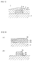
- the conventional ferroelectric memory 1 of this kind shown in Figure 13, includes a not-shown semiconductor substrate and a first insulation film 2 formed thereon. On the first insulation film 2, a lower electrode 3, a ferroelectric film 4 and an upper electrode 5 are formed in this order. Further, a second insulation film 6 is formed in a manner covering these films.
- a conductive film 3a is formed of platinum (Pt) or the like by sputtering over the first insulation film 2 formed on the semiconductor substrate, as shown in Figure 14(A). Then, a ferroelectric film 4a is formed of lead zirconate titanate (PZT) or the like on the conductive film 3a by a sol-gel process.
- Pt platinum
- PZT lead zirconate titanate
- a conductive film 5a is further formed by sputtering platinum (Pt) or the like over the ferroelectric film 4a. Then, as shown in Figure 14(B) dry etching is conducted sequentially on the conductive film 5a, the ferroelectric film 4a and the conductive film 3a, thereby providing an upper electrode 5, a ferroelectric film 4 and a lower electrode 3. Thereafter, an insulation film 6 ( Figure 13) is formed in a manner covering these films by a CVD process.
- a conductive film 5a, a ferroelectric film 4a and a conductive film 3a are formed to a thickness to provide an upper electrode 5, a ferroelectric film 4 and a lower electrode 3, so that dry etching is then conducted throughout a total film thickness in order to remove unwanted portions of these films,
- the prior art has required a much etch amount and hence a long etch time. This results in long-time exposure of the ferroelectric film 4 to the plasma atmosphere during a dry etch process.
- the plasma however has effects upon the ferroelectric 4 to lower its switching charge amount (Qsw).
- Qsw switching charge amount
- a ferroelectric memory comprises: an insulation film; a hollow formed in a top surface of the insulation film; a lower electrode formed in the hollow; a ferroelectric formed on the lower electrode; and an upper electrode formed on the ferroelectric.
- a manufacturing method is a method for manufacturing a ferroelectric memory having a lower electrode, ferroelectric and upper electrode formed on an insulation film, characterized in that a hollow is formed in a surface of the insulation film and then a lower electrode is formed in the hollow by a process including an application process.
- a hollow is formed in a top surface of an insulation film, and a lower electrode is formed in the hollow by a process including a spin coating method (e.g. sol-gel method).
- a spin coating method e.g. sol-gel method
- a precursor solution is dripped on the surface of the insulation film and splashed away by a centrifugal force. Consequently, the conductive film being formed has a thickness increased in a hollow portion that the precursor solution is ready to collect, i.e. a portion to be formed into a lower electrode, and decreased in other portion than the hollow. Accordingly, when etching the conductive film to form a lower electrode, it is satisfactory to etch only the portion other than the hollow, i.e.
- a resulting lower electrode is reduced in amount of a depression caused in a top surface center.
- a first electrode portion is formed at a hollow corner by a process including a spin coating method and further a second electrode portion is formed thereon by sputtering, a resulting lower electrode is reduced in variation of crystalline orientation thereof.
- the hollow will have a flat bottom surface at the predetermined depth position. Further, the film blocks the water content of the insulation film from reaching the ferroelectric through the lower electrode. Furthermore, if the lower electrode in the hollow and the insulation film at their top surfaces are planarized flush with each other, there is no necessity to etch the conductive film at portions other than the hollow in the later process. If a thin film is formed on a planarized lower electrode by using a same material as the lower electrode, eliminated is surface roughening caused on the lower electrode upon planarization.
- the ferroelectric can be prevented from being deteriorated in characteristics by a plasma effect.
- the ferroelectric can be stabilized in crystallinity and orientation by forming a first electrode portion at a hollow corner and a second electrode portion thereon to provide a lower electrode or by forming a thin film on a planarized lower electrode.
- the hollow can be made flat in its bottom surface in the predetermined depth, making possible to stably form a lower electrode.
- this film serves to block the moisture content of the insulation film from reaching the ferroelectric, thus preventing the ferroelectric from being deteriorated in characteristics.
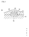
- a ferroelectric memory 10 of this embodiment which includes a first insulation film 12 formed on a not-shown silicon (Si) substrate.
- the first insulation film 12 has a hollow 14 formed in its top surface to have a lower electrode 16 inside the hollow 14.
- a ferroelectric 18 and an upper electrode 20 are formed on the lower electrode 16 in this order.
- a second insulation film 22 is formed covering these elements.
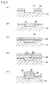
- a method for manufacturing a ferroelectric memory 10 will now be explained concretely with reference to Figure 2 and Figure 3.
- a not-shown silicon (Si) substrate is prepared, to form thereon by a CVD technique a first insulation film 12 of silicate glass containing phosphorus (PSG), silicate glass containing boron/phosphorus (BPSG) or the like.
- the first insulation film 12 is masked by a patterned resist 24 to form a hollow 14 by an RIE (reactive ion etching) technique as anisotropic dry etching.
- RIE reactive ion etching
- a first conductive film 26 as a gel dry film is formed by a sol-gel technique on a surface of the first insulation film 12 including an inside of the hollow 14. That is, an Ir precursor solution is formed by subjecting a metal alkoxide solution containing irridium (Ir) as an ingredient element to hydrolysis/polycondensation. This solution is applied onto a surface of the first insulation film 12 by a spin coating technique, and then dried into a gel dry film. In an application process using a spin coating technique, the precursor solution dripped on the surface of the first insulation film is splashed away due to a centrifugal force. However, the precursor solution existing inside the hollow 14 will not readily splashed away. This provides the first conductive film 26 with a film thickness that is greater at inside the hollow 14 than the other portion, as shown in Figure 2(B).
- a film 28 for providing a ferroelectric 18 is formed over a surface of the first conductive film 26 by the sol-gel technique, as shown in Figure 2(C). That is, a PZT (lead zirconate titanate) precursor solution is applied onto the surface of the first conductive film 26 by spin coating. The applied film is cured into a gel dry film. After forming the film 28, this structure overall is subjected to a heat process with utilizing RTA (Rapid Thermal Annealing) apparatus. The organic substances contained in the first conductive film 26 and film 28 are thermally decomposed and removed out of these films. Then, a second conductive film 30 is formed of platinum (Pt) over the film 28 by sputtering, as shown in Fig. 2(D).
- Pt platinum
- the second conductive film 30, the film 28 and the first conductive film 26 are sequentially etched (RIE technique) and removed of unwanted portions, as shown in Fig 2(E).
- the etch process requires to etch a total film thickness of the second conductive film and the film 28, i.e. by an amount for a thickness of an upper electrode 20 and ferroelectric 18. Nevertheless, it is satisfactory for the first conductive film 26 to be etched only at areas extending out of the hollow 14. As described before, the portion extending out of the hollow 14 is smaller in thickness than a lower electrode 16. For this reason, an etch time is reduced as compared to the prior art requiring to etch the entire thickness of a lower electrode 16.
- This structure is heat-processed using an RTA apparatus to bake and crystallize the first conductive film 26 and film 28.
- This provides a lower electrode 16 of irridium oxide (IrO 2 ) as well as a ferroelectric 18 of lead zirconate titanate (Pzt).
- the second conductive film 30 on the film 28 is formed of platinum (Pt) with preferential orientation. Accordingly, the crystallization in the ferroelectric 18 occurs in an orientation similar to that of the second conductive film 30. That is, the ferroelectric 18 can be controlled in orientation depending upon the second conductive film 30.
- a second insulation film 22 is formed of silicate glass containing phosphorus (PSG) or silicate glass containing boron/phosphorus covering these elements by CVD, as shown in Figure 1.
- a hollow 14 was formed in the top surface of the insulation film 12 so that a lower electrode 16 can be formed inside the hollow 14 by the sol-gel technique including a spin-coating application process.
- a lower electrode 16 can be formed inside the hollow 14 by the sol-gel technique including a spin-coating application process.
- the ferroelectric 18 can be prevented from being deteriorated in characteristics by the affection of a plasma.
- a ferroelectric memory 32 of another embodiment, shown in Figure 3, has a hole 34 formed through a second insulation film 22 covering a lower electrode 16, a ferroelectric 18 and an upper electrode 20. The hole is buried with an upper electrode 20.
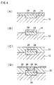
- a ferroelectric memory 32 spin coating is conducted to form a first conductive film 26 and film 28 over a first insulation film 12 formed with a hollow 14, as shown in Figure 4(A). Subsequently, as shown in Figure 4(B) etching is made (by an RIE technique) on the film 28 and first conductive film 26 to remove unwanted portions. The resulting structure is subjected to a heating process using an RTA apparatus. Then, a second insulation film 22 is formed in a manner covering the first conductive film 26 and film 28, as shown in Figure 4(C). The film 22 at its top surface is planarized by implementing a CMP (Chemical-Mechanical Polishing) technique.
- CMP Chemical-Mechanical Polishing
- etching is made (by RIE) on the second insulation film 22 to open a hole 34.
- a second conductive film 30 is formed over the second insulation film 22 in a manner filling this hole 34 by a spin coating technique (sol-gel technique).
- the second conductive film 30 and second insulation film 22 are planarized at top surfaces by the CMP (Chemical-Mechanical Polishing) technique.
- the resulting structure is subjected to heating process using an RTA apparatus to bake and crystallize the lower electrode 16, ferroelectric 18 and upper electrode 20.
- the planarization process may use etching in place of the CMP technique.
- the upper electrode 20 at its top surface is somewhat higher than a top surface of the second insulation film 22, as shown in Figure 5.
- the ferroelectric 18 can be prevented from being deteriorated in characteristic.
- the upper electrode 20 is buried in the hole 34, and further planarization is made for the top surfaces of the upper electrode 20 and second insulation film 22. It is therefore possible to form, on the second insulation film 22, an interconnect film in connection with the upper electrode 20.
- the first conductive film 26 portion extending out of the hollow 14 was removed by etching in the process of Figure 2(E) or Figure 4(B).
- this portion may be utilized for an interconnection 32 without being etched, as shown in Figure 6(A) or Figure 6(B).
- the film 28 was formed without planarizing the top surfaces of the first conductive film 26 and first insulation film 12.
- the film 28 may be formed after planarizing these top surfaces by a CMP (Chemical Mechanical Polishing) technique or etching.
- CMP Chemical Mechanical Polishing
- an etch time can be further shortened because of no necessity of etching the first conductive film 26 portion extending out of the hollow 14 in the later process.
- a thin film 36 may be formed on a surface of the planarized first conductive film 26 by using a same material as that of the first conductive film 26 as shown in Figure 8.
- a film 38 with a thickness of approximately 1000 angstroms may be formed of silicon nitride (Sin), silicon nitride oxide (SiON) or the like in a predetermined depth position of the first insulation film 12 so that this film 38 can be utilized as an etch stop for forming a hollow 14.
- the provision of a film 38 makes it possible to planarize a bottom surface of the hollow 14 at a predetermined depth. Accordingly, a lower electrode 16 ( Figure 1, Figure 3) can be stably formed on the bottom surface.
- This structure also serves to block the water content contained in the insulation film 12 below the film 38 from reaching the ferroelectric 18 thorough the lower electrode 16. It is therefore possible to prevent the ferroelectric 18 ( Figure 1, Figure 3) from being deteriorated in characteristic by the water content effect.
- a first electrode portion 16a may be formed at a corner of the hollow 14 by a process including spin coating (e.g. sol-gel technique)so that a second electrode portion 16b can be formed to provide a lower electrode 16.
- spin coating e.g. sol-gel technique
- the second electrode portion 16b is formed by a process including a spin coat technique (e.g. sol-gel technique)
- the second electrode portion 16b, or first conductive film 26b is formed by sputtering, the variation in crystalline orientation is reduced in a top surface of the lower electrode 16, as shown in Figure 11.
- the second electrode portion 16b can be made thin in thickness by a corresponding amount to the film thickness of the first electrode portion 16a. This reduce the amount of etching to be conductede in the etching process.
- the lower electrode 16 may use ruthenium oxide (RuO 2 ), rhodium oxide (RhO 2 ) or palladium oxide (PdO 2 ) in place of irridium oxide (IrO 2 ).
- ruthenium oxide RuO 2
- RhO 2 rhodium oxide
- PdO 2 palladium oxide
- a precursor solution is formed containing an ingredient element of ruthenium (Ru), rhodium (Rh), palladium (Pd) or the like.
- the lower electrode 16 and upper electrode 20 were formed by the sol-gel technique, they may be formed by another process including spin coat process, such as in an MOD method (organic-metal decomposition).
Landscapes
- Semiconductor Memories (AREA)
Applications Claiming Priority (2)
| Application Number | Priority Date | Filing Date | Title |
|---|---|---|---|
| JP34132698 | 1998-12-01 | ||
| JP34132698A JP4416055B2 (ja) | 1998-12-01 | 1998-12-01 | 強誘電体メモリおよびその製造方法 |
Publications (1)
| Publication Number | Publication Date |
|---|---|
| EP1006590A1 true EP1006590A1 (de) | 2000-06-07 |
Family
ID=18345200
Family Applications (1)
| Application Number | Title | Priority Date | Filing Date |
|---|---|---|---|
| EP99123866A Withdrawn EP1006590A1 (de) | 1998-12-01 | 1999-12-01 | Ferroelektrischer Speicher und Verfahren zur Herstellung |
Country Status (3)
| Country | Link |
|---|---|
| US (2) | US6900486B1 (de) |
| EP (1) | EP1006590A1 (de) |
| JP (1) | JP4416055B2 (de) |
Families Citing this family (7)
| Publication number | Priority date | Publication date | Assignee | Title |
|---|---|---|---|---|
| US7672558B2 (en) | 2004-01-12 | 2010-03-02 | Honeywell International, Inc. | Silicon optical device |
| ES2211366B1 (es) * | 2004-03-18 | 2005-03-01 | Miguel Jose Maldonado Lopez | Plataforma de ablacion posterior para lasik. |
| US7808024B2 (en) * | 2004-09-27 | 2010-10-05 | Intel Corporation | Ferroelectric polymer memory module |
| US7362443B2 (en) | 2005-11-17 | 2008-04-22 | Honeywell International Inc. | Optical gyro with free space resonator and method for sensing inertial rotation rate |
| US7463360B2 (en) * | 2006-04-18 | 2008-12-09 | Honeywell International Inc. | Optical resonator gyro with integrated external cavity beam generator |
| US7454102B2 (en) | 2006-04-26 | 2008-11-18 | Honeywell International Inc. | Optical coupling structure |
| US7535576B2 (en) * | 2006-05-15 | 2009-05-19 | Honeywell International, Inc. | Integrated optical rotation sensor and method for sensing rotation rate |
Citations (7)
| Publication number | Priority date | Publication date | Assignee | Title |
|---|---|---|---|---|
| JPH05327062A (ja) * | 1992-05-22 | 1993-12-10 | Sharp Corp | 強誘電体記憶素子 |
| EP0697719A2 (de) * | 1994-08-01 | 1996-02-21 | Texas Instruments Incorporated | Mikroelektronische Struktur mit einer Sperrschicht aus leitendem exotischen Nitrid für Elektroden mit einer hohen Dielektrizitätskonstante und Verfahren zu deren Herstellung |
| US5652446A (en) * | 1994-09-20 | 1997-07-29 | Nec Corporation | Semiconductor memory device with improved capacitor |
| US5801916A (en) * | 1995-11-13 | 1998-09-01 | Micron Technology, Inc. | Pre-patterned contact fill capacitor for dielectric etch protection |
| US5807774A (en) * | 1996-12-06 | 1998-09-15 | Sharp Kabushiki Kaisha | Simple method of fabricating ferroelectric capacitors |
| EP0886317A2 (de) * | 1997-06-16 | 1998-12-23 | Sanyo Electric Co. Ltd | Ferroelektrische Vorrichtung, nichtflüchtiger Halbleiterspeicher und Verfahren zu ihrer Herstellung |
| JPH11251549A (ja) * | 1998-03-06 | 1999-09-17 | Asahi Chem Ind Co Ltd | 強誘電体容量素子の形成方法 |
Family Cites Families (10)
| Publication number | Priority date | Publication date | Assignee | Title |
|---|---|---|---|---|
| GB2164047B (en) * | 1984-08-21 | 1989-05-24 | Secr Defence | Polymeric electrolytes |
| JPH0499057A (ja) * | 1990-08-07 | 1992-03-31 | Seiko Epson Corp | 半導体装置とその製造方法 |
| JPH0697719A (ja) | 1992-03-26 | 1994-04-08 | Nec Corp | アンテナのジャッキ駆動装置の固定機構 |
| JP3407204B2 (ja) * | 1992-07-23 | 2003-05-19 | オリンパス光学工業株式会社 | 強誘電体集積回路及びその製造方法 |
| KR950009813B1 (ko) * | 1993-01-27 | 1995-08-28 | 삼성전자주식회사 | 반도체장치 및 그 제조방법 |
| US5614438A (en) * | 1995-03-15 | 1997-03-25 | Radiant Technologies, Inc. | Method for making LSCO stack electrode |
| JP3279453B2 (ja) * | 1995-03-20 | 2002-04-30 | シャープ株式会社 | 不揮発性ランダムアクセスメモリ |
| JP3368726B2 (ja) * | 1995-08-07 | 2003-01-20 | ヤマハ株式会社 | 半導体記憶装置とその製造方法 |
| KR100215867B1 (ko) * | 1996-04-12 | 1999-08-16 | 구본준 | 반도체 소자의 커패시터 구조 및 제조 방법 |
| US6297085B1 (en) * | 1997-12-11 | 2001-10-02 | Texas Instruments Incorporated | Method for manufacturing ferroelectric capacitor and method for manufacturing ferroelectric memory |
-
1998
- 1998-12-01 JP JP34132698A patent/JP4416055B2/ja not_active Expired - Fee Related
-
1999
- 1999-11-30 US US09/451,979 patent/US6900486B1/en not_active Expired - Lifetime
- 1999-12-01 EP EP99123866A patent/EP1006590A1/de not_active Withdrawn
-
2001
- 2001-08-14 US US09/929,187 patent/US6656747B2/en not_active Expired - Lifetime
Patent Citations (7)
| Publication number | Priority date | Publication date | Assignee | Title |
|---|---|---|---|---|
| JPH05327062A (ja) * | 1992-05-22 | 1993-12-10 | Sharp Corp | 強誘電体記憶素子 |
| EP0697719A2 (de) * | 1994-08-01 | 1996-02-21 | Texas Instruments Incorporated | Mikroelektronische Struktur mit einer Sperrschicht aus leitendem exotischen Nitrid für Elektroden mit einer hohen Dielektrizitätskonstante und Verfahren zu deren Herstellung |
| US5652446A (en) * | 1994-09-20 | 1997-07-29 | Nec Corporation | Semiconductor memory device with improved capacitor |
| US5801916A (en) * | 1995-11-13 | 1998-09-01 | Micron Technology, Inc. | Pre-patterned contact fill capacitor for dielectric etch protection |
| US5807774A (en) * | 1996-12-06 | 1998-09-15 | Sharp Kabushiki Kaisha | Simple method of fabricating ferroelectric capacitors |
| EP0886317A2 (de) * | 1997-06-16 | 1998-12-23 | Sanyo Electric Co. Ltd | Ferroelektrische Vorrichtung, nichtflüchtiger Halbleiterspeicher und Verfahren zu ihrer Herstellung |
| JPH11251549A (ja) * | 1998-03-06 | 1999-09-17 | Asahi Chem Ind Co Ltd | 強誘電体容量素子の形成方法 |
Non-Patent Citations (2)
| Title |
|---|
| PATENT ABSTRACTS OF JAPAN vol. 18, no. 144 (E - 1521) 10 March 1994 (1994-03-10) * |
| PATENT ABSTRACTS OF JAPAN vol. 1999, no. 14 22 December 1999 (1999-12-22) * |
Also Published As
| Publication number | Publication date |
|---|---|
| JP2000174223A (ja) | 2000-06-23 |
| JP4416055B2 (ja) | 2010-02-17 |
| US6656747B2 (en) | 2003-12-02 |
| US6900486B1 (en) | 2005-05-31 |
| US20020005532A1 (en) | 2002-01-17 |
Similar Documents
| Publication | Publication Date | Title |
|---|---|---|
| TWI270178B (en) | Ferroelectric random access memory capacitor and method for manufacturing the same | |
| KR100346668B1 (ko) | 절연측벽캐패시터 | |
| US6284589B1 (en) | Method of fabricating concave capacitor including adhesion spacer | |
| US7041570B2 (en) | Method of forming a capacitor | |
| US5774327A (en) | High dielectric capacitors | |
| JPH1041478A (ja) | 電気デバイスおよび複合スタック電極の作製方法 | |
| JPH08316430A (ja) | 半導体メモリとその製造方法、スタックドキャパシタ | |
| JP2000150810A (ja) | 半導体装置及びその製造方法 | |
| US6335287B1 (en) | Method of forming trench isolation regions | |
| US6656747B2 (en) | Ferroelectric memory and method for manufacturing same | |
| US6131258A (en) | Sidewall capacitor with L-shaped dielectric | |
| WO1997035341A1 (fr) | Dispositif de stockage a semi-conducteur et sa production | |
| US6242321B1 (en) | Structure and fabrication method for non-planar memory elements | |
| US5874336A (en) | Method to improve yield for capacitors formed using etchback of polysilicon hemispherical grains | |
| US20050206469A1 (en) | Interdigitated capacitor and method for fabrication therof | |
| JPH10107223A (ja) | 誘電体キャパシタ及び誘電体メモリ装置と、これらの製造方法 | |
| US6534377B2 (en) | Capacitance elements and method of manufacturing the same | |
| US20010024862A1 (en) | Method for forming a lower electrode by using an electroplating method | |
| US6414344B1 (en) | Semiconductor device for use in a memory cell and method for the manufacture thereof | |
| US5420077A (en) | Method for forming a wiring layer | |
| US6335206B1 (en) | Integrated capacitor device and method of fabricating the same | |
| KR100230402B1 (ko) | 반도체소자의 커패시터 및 그 제조방법 | |
| JP2000223464A (ja) | 基板洗浄方法 | |
| US7183121B2 (en) | Process for fabrication of a ferrocapacitor | |
| KR20000044893A (ko) | 반도체 소자의 캐패시터 제조 방법 |
Legal Events
| Date | Code | Title | Description |
|---|---|---|---|
| PUAI | Public reference made under article 153(3) epc to a published international application that has entered the european phase |
Free format text: ORIGINAL CODE: 0009012 |
|
| AK | Designated contracting states |
Kind code of ref document: A1 Designated state(s): DE FR GB NL |
|
| AX | Request for extension of the european patent |
Free format text: AL;LT;LV;MK;RO;SI |
|
| 17P | Request for examination filed |
Effective date: 20001020 |
|
| AKX | Designation fees paid |
Free format text: DE FR GB NL |
|
| STAA | Information on the status of an ep patent application or granted ep patent |
Free format text: STATUS: THE APPLICATION HAS BEEN WITHDRAWN |
|
| 18W | Application withdrawn |
Effective date: 20091229 |