EP0697731A2 - Flachgehäuse für Halbleiter-IC - Google Patents
Flachgehäuse für Halbleiter-IC Download PDFInfo
- Publication number
- EP0697731A2 EP0697731A2 EP19950112887 EP95112887A EP0697731A2 EP 0697731 A2 EP0697731 A2 EP 0697731A2 EP 19950112887 EP19950112887 EP 19950112887 EP 95112887 A EP95112887 A EP 95112887A EP 0697731 A2 EP0697731 A2 EP 0697731A2
- Authority
- EP
- European Patent Office
- Prior art keywords
- leads
- suspension leads
- cavity
- flat package
- substrate
- Prior art date
- Legal status (The legal status is an assumption and is not a legal conclusion. Google has not performed a legal analysis and makes no representation as to the accuracy of the status listed.)
- Granted
Links
Images





Classifications
-
- H—ELECTRICITY
- H10—SEMICONDUCTOR DEVICES; ELECTRIC SOLID-STATE DEVICES NOT OTHERWISE PROVIDED FOR
- H10W—GENERIC PACKAGES, INTERCONNECTIONS, CONNECTORS OR OTHER CONSTRUCTIONAL DETAILS OF DEVICES COVERED BY CLASS H10
- H10W74/00—Encapsulations, e.g. protective coatings
-
- H—ELECTRICITY
- H10—SEMICONDUCTOR DEVICES; ELECTRIC SOLID-STATE DEVICES NOT OTHERWISE PROVIDED FOR
- H10W—GENERIC PACKAGES, INTERCONNECTIONS, CONNECTORS OR OTHER CONSTRUCTIONAL DETAILS OF DEVICES COVERED BY CLASS H10
- H10W76/00—Containers; Fillings or auxiliary members therefor; Seals
- H10W76/10—Containers or parts thereof
- H10W76/12—Containers or parts thereof characterised by their shape
- H10W76/15—Containers comprising an insulating or insulated base
- H10W76/157—Containers comprising an insulating or insulated base having interconnections parallel to the insulating or insulated base
-
- H—ELECTRICITY
- H10—SEMICONDUCTOR DEVICES; ELECTRIC SOLID-STATE DEVICES NOT OTHERWISE PROVIDED FOR
- H10W—GENERIC PACKAGES, INTERCONNECTIONS, CONNECTORS OR OTHER CONSTRUCTIONAL DETAILS OF DEVICES COVERED BY CLASS H10
- H10W42/00—Arrangements for protection of devices
- H10W42/20—Arrangements for protection of devices protecting against electromagnetic or particle radiation, e.g. light, X-rays, gamma-rays or electrons
-
- H—ELECTRICITY
- H10—SEMICONDUCTOR DEVICES; ELECTRIC SOLID-STATE DEVICES NOT OTHERWISE PROVIDED FOR
- H10W—GENERIC PACKAGES, INTERCONNECTIONS, CONNECTORS OR OTHER CONSTRUCTIONAL DETAILS OF DEVICES COVERED BY CLASS H10
- H10W90/00—Package configurations
- H10W90/701—Package configurations characterised by the relative positions of pads or connectors relative to package parts
-
- H—ELECTRICITY
- H10—SEMICONDUCTOR DEVICES; ELECTRIC SOLID-STATE DEVICES NOT OTHERWISE PROVIDED FOR
- H10W—GENERIC PACKAGES, INTERCONNECTIONS, CONNECTORS OR OTHER CONSTRUCTIONAL DETAILS OF DEVICES COVERED BY CLASS H10
- H10W70/00—Package substrates; Interposers; Redistribution layers [RDL]
- H10W70/60—Insulating or insulated package substrates; Interposers; Redistribution layers
- H10W70/67—Insulating or insulated package substrates; Interposers; Redistribution layers characterised by their insulating layers or insulating parts
- H10W70/68—Shapes or dispositions thereof
- H10W70/682—Shapes or dispositions thereof comprising holes having chips therein
-
- H—ELECTRICITY
- H10—SEMICONDUCTOR DEVICES; ELECTRIC SOLID-STATE DEVICES NOT OTHERWISE PROVIDED FOR
- H10W—GENERIC PACKAGES, INTERCONNECTIONS, CONNECTORS OR OTHER CONSTRUCTIONAL DETAILS OF DEVICES COVERED BY CLASS H10
- H10W70/00—Package substrates; Interposers; Redistribution layers [RDL]
- H10W70/60—Insulating or insulated package substrates; Interposers; Redistribution layers
- H10W70/67—Insulating or insulated package substrates; Interposers; Redistribution layers characterised by their insulating layers or insulating parts
- H10W70/68—Shapes or dispositions thereof
- H10W70/685—Shapes or dispositions thereof comprising multiple insulating layers
-
- H—ELECTRICITY
- H10—SEMICONDUCTOR DEVICES; ELECTRIC SOLID-STATE DEVICES NOT OTHERWISE PROVIDED FOR
- H10W—GENERIC PACKAGES, INTERCONNECTIONS, CONNECTORS OR OTHER CONSTRUCTIONAL DETAILS OF DEVICES COVERED BY CLASS H10
- H10W72/00—Interconnections or connectors in packages
- H10W72/50—Bond wires
- H10W72/541—Dispositions of bond wires
- H10W72/5445—Dispositions of bond wires being orthogonal to a side surface of the chip, e.g. parallel arrangements
-
- H—ELECTRICITY
- H10—SEMICONDUCTOR DEVICES; ELECTRIC SOLID-STATE DEVICES NOT OTHERWISE PROVIDED FOR
- H10W—GENERIC PACKAGES, INTERCONNECTIONS, CONNECTORS OR OTHER CONSTRUCTIONAL DETAILS OF DEVICES COVERED BY CLASS H10
- H10W72/00—Interconnections or connectors in packages
- H10W72/50—Bond wires
- H10W72/551—Materials of bond wires
- H10W72/552—Materials of bond wires comprising metals or metalloids, e.g. silver
-
- H—ELECTRICITY
- H10—SEMICONDUCTOR DEVICES; ELECTRIC SOLID-STATE DEVICES NOT OTHERWISE PROVIDED FOR
- H10W—GENERIC PACKAGES, INTERCONNECTIONS, CONNECTORS OR OTHER CONSTRUCTIONAL DETAILS OF DEVICES COVERED BY CLASS H10
- H10W90/00—Package configurations
- H10W90/701—Package configurations characterised by the relative positions of pads or connectors relative to package parts
- H10W90/751—Package configurations characterised by the relative positions of pads or connectors relative to package parts of bond wires
- H10W90/754—Package configurations characterised by the relative positions of pads or connectors relative to package parts of bond wires between a chip and a stacked insulating package substrate, interposer or RDL
Definitions
- the present invention relates to a flat package for a semiconductor IC (Integrated Circuit) and, more particularly, to a quad flat package having leads extending out in four directions.
- a flat package for a semiconductor IC is disclosed in, for example, "LSI Handbook" compiled by the Institute of Electronic and Communication Engineers of Japan and published by Ohm Sha, 1984, pp. 414-415. This document shows, particularly in Figure 3 ⁇ 62, a typical surface mounting package having leads extending out from all the four sides thereof. This type of package is generally referred to as a quad flat package (QFP).
- QFP quad flat package
- a flat package has been developed to implement the miniaturization and advanced functions of various kinds of electronic apparatuses, and is extensively used today.
- a QFP in particular facilitates impedance matching because it has a substantially square contour, i.e., all the wirings in the package have substantially the same length.
- a semiconductor chip mounted on the package should be shielded in order to be immune to external electromagnetic fields and to radiate no needless electromagnetic waves to the outside, i.e., to enhance the electromagnetic wave interference (EMI) characteristic.
- EMI electromagnetic wave interference
- an object of the present invention to provide a flat package for a semiconductor IC and capable of meeting the users' different needs relating to shield connection with a single standard type of ICs without limiting the number of valid leads.
- a flat package for a semiconductor IC of the present invention has a substrate having a metallized cavity for mounting a semiconductor chip, and a seal metallized portion for sealing a metallic cap for hermetic sealing.
- a lead frame has a quadrilateral frame, and four suspension leads respectively positioned at four corners of the frame for holding the substrate at the center of the frame.
- the substrate additionally has a first internal wiring for grounding and second internal wirings for grounding respectively connecting the cavity and the seal metallized portion to the suspension leads.
- the flat package is shown in a condition before hermetic sealing.
- the package is generally made up of a semiconductor chip 1, a substrate 2, and a lead frame 5.
- the substrate 2 is implemented as a ceramic or plastic laminate substrate including a wiring layer for electric connection, not shown.
- the substrate 2 has a cavity 21 and a seal metallized portion 22.
- the cavity 21, receiving the chip 1 therein, is metallized for conductivity.
- a metallic cap for hermetic sealing, not shown, is fitted on the seal metallized portion 22.
- the lead frame 5 has suspension leads 3 at four corners thereof for holding the substrate 2, leads 4 for connecting the package to external circuitry, and a tiebar or frame 51.
- Guide holes 52 are formed in the tiebar 51. After the leads 4 have been cut off from the tiebar 51, the electric characteristic of the IC is tested with the leads 4 held in their contact positions by the guide holes 52, as will be described specifically later. During this test, the suspension leads 3 additionally serve to hold the tiebar 51.
- the IC is packaged and sealed by the following procedure.
- the chip 1 is bonded to the cavity 21 of the substrate 2 by conductive adhesive.
- Electrode pads, not shown, provided on the chip 1 are respectively connected to the leads 4 by metallic wires via the wiring layer of the substrate 2.
- the metallic cap is soldered to the seal metallized portion 22, thereby hermetically sealing the chip 1.
- the leads 4 other than the suspension leads 3 are cut off from the tiebar 51.
- the guide holes 52 of the tiebar 51 are respectively coupled over guide pins provided on a testing jig. Hence, the leads 4 are accurately connected to corresponding contacts also provided on the testing jig. If the IC is acceptable as determined by the test, the suspension leads 3 are cut off to remove the tiebar 51. Finally, the leads 4 are each trimmed to have a predetermined shape.
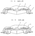
- the suspension leads 3 appear as shown either in FIG. 2A or in FIG. 2B.
- the suspension leads 3 are usually removed and, therefore, make no contribution to the electrical connection of the IC to external circuitry.
- the flat package having the above configuration is extensively used in a logical circuit having a high degree of integration and needing high-speed performance.
- the chip 1 should be shielded in order to be immune to external electromagnetic fields and to radiate no needless electromagnetic waves to the outside, i.e., to enhance the EMI characteristic. This has customarily been done by connecting the cavity 21 and seal metallized portion 22 to ground.
- one or both of the cavity 21 and seal metallized portion 22 are respectively connected to, among the leads 4, the leads 4 preselected for this purpose by exclusive wirings.
- the problem is that the number of leads 4 is limited by the relation between the lead pitch and the dimensions of the substrate 2.
- the exclusive leads 4 for shielding are not always guaranteed due to the required number of leads for electrical connection which is increasing to implement advanced functions. It is, therefore, a common practice to connect, within the substrate 2, one or both of the cavity 21 and shield metallized portion 22 to any one of ground wirings laid in the chip 1, depending on the user's desired specifications.
- a plurality of ground wirings exist in the chip 1. This, coupled with the combination of the cavity 21 and seal metallized portion 22, results in a great number of combinations of internal ground connections using the internal wirings. Hence, when a plurality of users each desires different specifications as to the ground connection, the supplier must prepare a plurality of ICs which are identical in configuration except for the shield, but different in type.
- Japanese Patent Laid-Open Publication No. 62-45156 discloses a package for a semiconductor device and having a lead frame including tab suspension leads.
- the lead frame electrically connects a semiconductor chip mounted on a ceramic package to the terminals of external circuitry.
- the chip is bonded to a tab also included in the lead frame by conductive adhesive while the tab is electrically connected to the tab suspension leads, thereby substantially connecting the chip to ground.
- This successfully connects the chip to ground for the shielding purpose without resorting to extra leads and thereby enhances the stable operation of the IC.
- the lead frame having the tab is for use in a ceramic package which accommodates a small scale IC having a small number of leads, it is not directly applicable to the previously stated flat package.
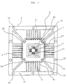
- a flat package embodying the present invention is shown in a condition before hermetic sealing.
- the package has a semiconductor chip 1 common to the previously stated chip 1, a substrate 2A replacing the conventional substrate 2, and a lead frame 5A replacing the conventional lead frame 5.
- the substrate 2A additionally has internal wirings 23 and 24 respectively connecting a cavity 21 and a seal metallized portion 22 to external circuitry.
- the lead frame 5A includes suspension leads 3A 3C connected to the wiring 23 and suspension leads 3B and 3D respectively connected to the wirings 24.
- the package is designed such that when the distance between nearby leads 4 is 0.5 mm, the leads 4 are 0.2 mm wide each while the suspension leads 3A-3D are 0.5 mm wide each.
- the suspension leads 3A-3D, having a greater width than the leads 4, are capable of surely holding the leads 4 in the event of a selection test.
- the flat package having the above configuration is sealed by the conventional procedure. Thereafter, the leads 4 other than the suspension leads 3A-3D are cut off from a tiebar 51. In this condition, the conventional electric characteristic test for selection is performed.
- the suspension leads 3A-3D serving to connect the package and tiebar 51 in the event of the test, may be configured as shown in FIG. 7.
- the previous embodiment is advantageous over this embodiment in that the leads 3A-3D of the former protect the outermost leads 4, which often receive the greatest signals, from deformation attributable to extraneous impacts more positively than the leads 3A-3D of the latter. This is because the leads 3A-3D of FIG. 3 each extends perpendicularly to the edge of the package.
- the package proved to be acceptable by the test, has its suspension leads 3A-3D cut off in the vicinity of the tiebar 51, so that the tiebar 51 is removed. Finally, the suspension leads 3A-3D are trimmed in the same manner as the leads 4.
- FIG. 4 shows the leads 4 and suspension lead 3A (3B,3C or 3D) in a trimmed condition.
- the lead 3A physically protects the outermost leads 41 from extraneous stresses.
- the suspension lead 3A is connected to the internal wiring 23 connected to the cavity 21.
- the suspension leads 3A and 3C and/or the suspension leads 3B and 3D may be connected to a power supply assigned to the IC, because the grounding for shielding should only be implemented by a ground potential as to high frequency. In this manner, the IC can be optimally shielded on a circuit board by having one or both of the suspension leads 3A and 3C and the suspension leads 3B and 3D connected to ground or to a power supply assigned thereto.
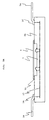
- FIGS. 5 and 5A show the flat package of the embodiment in a hermetically sealed condition.
- the reference numeral 6 designates a cap.
- FIGS. 8A and 8B show another alternative embodiment of the present invention in a hermetically sealed condition.
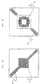
- FIGS. 9A and 9B show internal wiring layers particular to this embodiment.
- the suspension leads 3A and 3C are connected to the cavity 21 by a plain wiring.
- the suspension leads 3B and 3D are connected to the seal metallized portion 22 by a plain wiring.
- signal wirings laid in the package are also shielded. This further enhances the EMI characteristic, i.e., isolates the chip from external electromagnetic fields and causes no needless electromagnetic waves to be radiated to the outside.
- a flat package in accordance with the present invention, includes a substrate having internal ground wirings respectively connecting a cavity and a seal metallized portion to respective suspension leads.
- the suspension leads are connected to ground for a shielding purpose.
- the package eliminates the need for exclusive ground leads which would limit the number of available valid leads.
- a single standard type of ICs can implement various shield configurations as desired by users.
Landscapes
- Lead Frames For Integrated Circuits (AREA)
- Shielding Devices Or Components To Electric Or Magnetic Fields (AREA)
Applications Claiming Priority (3)
| Application Number | Priority Date | Filing Date | Title |
|---|---|---|---|
| JP19261394 | 1994-08-16 | ||
| JP192613/94 | 1994-08-16 | ||
| JP19261394A JP2594762B2 (ja) | 1994-08-16 | 1994-08-16 | フラットパッケージ |
Publications (3)
| Publication Number | Publication Date |
|---|---|
| EP0697731A2 true EP0697731A2 (de) | 1996-02-21 |
| EP0697731A3 EP0697731A3 (de) | 1997-07-16 |
| EP0697731B1 EP0697731B1 (de) | 2002-11-20 |
Family
ID=16294178
Family Applications (1)
| Application Number | Title | Priority Date | Filing Date |
|---|---|---|---|
| EP19950112887 Expired - Lifetime EP0697731B1 (de) | 1994-08-16 | 1995-08-16 | Flachgehäuse für Halbleiter-IC |
Country Status (5)
| Country | Link |
|---|---|
| US (1) | US5616954A (de) |
| EP (1) | EP0697731B1 (de) |
| JP (1) | JP2594762B2 (de) |
| KR (1) | KR0178567B1 (de) |
| DE (1) | DE69528869T2 (de) |
Families Citing this family (9)
| Publication number | Priority date | Publication date | Assignee | Title |
|---|---|---|---|---|
| US5861667A (en) * | 1997-03-11 | 1999-01-19 | Texas Instruments Incorporated | Single end in out arrangement |
| JPH10288625A (ja) * | 1997-04-15 | 1998-10-27 | Mitsubishi Electric Corp | 半導体加速度検出装置 |
| US6025616A (en) * | 1997-06-25 | 2000-02-15 | Honeywell Inc. | Power distribution system for semiconductor die |
| US5903051A (en) * | 1998-04-03 | 1999-05-11 | Motorola, Inc. | Electronic component and method of manufacture |
| JP4072505B2 (ja) * | 2003-02-28 | 2008-04-09 | エルピーダメモリ株式会社 | 積層型半導体パッケージ |
| US7563646B2 (en) * | 2007-05-31 | 2009-07-21 | Stratedge Corporation | Molded ceramic surface mount package |
| TWI405313B (zh) * | 2010-03-31 | 2013-08-11 | Quanta Comp Inc | 具側邊接腳之積體電路封裝元件 |
| US8525321B2 (en) | 2011-07-06 | 2013-09-03 | Fairchild Semiconductor Corporation | Conductive chip disposed on lead semiconductor package |
| CN102437061A (zh) * | 2011-11-30 | 2012-05-02 | 深圳市威怡电气有限公司 | 电子元件及其封装方法 |
Citations (1)
| Publication number | Priority date | Publication date | Assignee | Title |
|---|---|---|---|---|
| JPS6245156A (ja) | 1985-08-23 | 1987-02-27 | Hitachi Ltd | 気密封止電子装置 |
Family Cites Families (11)
| Publication number | Priority date | Publication date | Assignee | Title |
|---|---|---|---|---|
| JPS5521110A (en) * | 1978-08-02 | 1980-02-15 | Oki Electric Ind Co Ltd | Package for accommodating semiconductor parts |
| US4972253A (en) * | 1988-06-27 | 1990-11-20 | Digital Equipment Corporation | Programmable ceramic high performance custom package |
| JPH0281459A (ja) * | 1988-09-16 | 1990-03-22 | Sumitomo Electric Ind Ltd | Icパッケージ |
| JPH03256351A (ja) * | 1990-03-06 | 1991-11-15 | Nec Corp | 半導体装置 |
| US5043534A (en) * | 1990-07-02 | 1991-08-27 | Olin Corporation | Metal electronic package having improved resistance to electromagnetic interference |
| US5168344A (en) * | 1990-08-15 | 1992-12-01 | W. R. Grace & Co. Conn. | Ceramic electronic package design |
| JPH0498857A (ja) * | 1990-08-16 | 1992-03-31 | Nec Kyushu Ltd | 半導体装置用パッケージ |
| JP3009788B2 (ja) * | 1991-11-15 | 2000-02-14 | 日本特殊陶業株式会社 | 集積回路用パッケージ |
| EP0547807A3 (en) * | 1991-12-16 | 1993-09-22 | General Electric Company | Packaged electronic system |
| JP3105089B2 (ja) * | 1992-09-11 | 2000-10-30 | 株式会社東芝 | 半導体装置 |
| JP2912779B2 (ja) * | 1992-11-26 | 1999-06-28 | 京セラ株式会社 | 半導体素子収納用パッケージの製造方法 |
-
1994
- 1994-08-16 JP JP19261394A patent/JP2594762B2/ja not_active Expired - Fee Related
-
1995
- 1995-08-14 KR KR1019950025019A patent/KR0178567B1/ko not_active Expired - Fee Related
- 1995-08-16 US US08/515,600 patent/US5616954A/en not_active Expired - Fee Related
- 1995-08-16 DE DE1995628869 patent/DE69528869T2/de not_active Expired - Fee Related
- 1995-08-16 EP EP19950112887 patent/EP0697731B1/de not_active Expired - Lifetime
Patent Citations (1)
| Publication number | Priority date | Publication date | Assignee | Title |
|---|---|---|---|---|
| JPS6245156A (ja) | 1985-08-23 | 1987-02-27 | Hitachi Ltd | 気密封止電子装置 |
Non-Patent Citations (1)
| Title |
|---|
| "LSI Handbook", 1984, OHM SHA, pages: 414 - 415 |
Also Published As
| Publication number | Publication date |
|---|---|
| DE69528869D1 (de) | 2003-01-02 |
| DE69528869T2 (de) | 2004-02-26 |
| JPH0855949A (ja) | 1996-02-27 |
| EP0697731B1 (de) | 2002-11-20 |
| US5616954A (en) | 1997-04-01 |
| KR960009132A (ko) | 1996-03-22 |
| KR0178567B1 (ko) | 1999-03-20 |
| JP2594762B2 (ja) | 1997-03-26 |
| EP0697731A3 (de) | 1997-07-16 |
Similar Documents
| Publication | Publication Date | Title |
|---|---|---|
| US5581122A (en) | Packaging assembly with consolidated common voltage connections for integrated circuits | |
| US5734198A (en) | Multi-layer lead frame for a semiconductor device | |
| EP0564865A1 (de) | Halbleiteranordnung mit Kontakten für Testzwecke und Herstellungsmethode für dieselben | |
| US5225709A (en) | Package having a structure for stabilizing and/or impedance-matching a semiconductor IC device accommodated therein | |
| US20030197250A1 (en) | Semiconductor device and method of fabricating the same | |
| US5789816A (en) | Multiple-chip integrated circuit package including a dummy chip | |
| US5965936A (en) | Multi-layer lead frame for a semiconductor device | |
| WO2003023850A1 (en) | Semiconductor package | |
| EP0484062B1 (de) | Eine Halbleiteranordnung mit zwei integrierten Schaltungspackungen | |
| EP0697731B1 (de) | Flachgehäuse für Halbleiter-IC | |
| US6781223B2 (en) | Semiconductor device having a signal lead exposed on the undersurface of a sealing resin with an air gap between the signal lead and a mounting substrate | |
| US6847115B2 (en) | Packaged semiconductor device for radio frequency shielding | |
| US6998292B2 (en) | Apparatus and method for inter-chip or chip-to-substrate connection with a sub-carrier | |
| JPH0752759B2 (ja) | パツケ−ジ | |
| KR19990029106A (ko) | 갈륨 아세나이드 집적회로용 와이어본딩 되지 않은 입/출력 인터페이스 | |
| US20030151123A1 (en) | Semiconductor die package having two die paddles | |
| JP3150560B2 (ja) | 半導体装置 | |
| US7339269B2 (en) | High frequency IC package, high frequency unit using high frequency IC package, and manufacturing method thereof | |
| JP2000183488A (ja) | ハイブリッドモジュール | |
| JPH10107091A (ja) | 電子部品の実装構造およびその製造方法 | |
| EP0656741A2 (de) | Halbleitergehäusung | |
| JP2643898B2 (ja) | 樹脂封止型半導体装置およびその製造方法 | |
| JPH06260568A (ja) | Icソケット | |
| JPH04216653A (ja) | 半導体集積回路用パッケージおよびその実装方法 | |
| JPH09307012A (ja) | 半導体パッケージ |
Legal Events
| Date | Code | Title | Description |
|---|---|---|---|
| PUAI | Public reference made under article 153(3) epc to a published international application that has entered the european phase |
Free format text: ORIGINAL CODE: 0009012 |
|
| AK | Designated contracting states |
Kind code of ref document: A2 Designated state(s): DE FR GB |
|
| PUAL | Search report despatched |
Free format text: ORIGINAL CODE: 0009013 |
|
| AK | Designated contracting states |
Kind code of ref document: A3 Designated state(s): DE FR GB |
|
| 17P | Request for examination filed |
Effective date: 19970611 |
|
| 17Q | First examination report despatched |
Effective date: 19981014 |
|
| GRAG | Despatch of communication of intention to grant |
Free format text: ORIGINAL CODE: EPIDOS AGRA |
|
| GRAG | Despatch of communication of intention to grant |
Free format text: ORIGINAL CODE: EPIDOS AGRA |
|
| GRAH | Despatch of communication of intention to grant a patent |
Free format text: ORIGINAL CODE: EPIDOS IGRA |
|
| GRAH | Despatch of communication of intention to grant a patent |
Free format text: ORIGINAL CODE: EPIDOS IGRA |
|
| GRAA | (expected) grant |
Free format text: ORIGINAL CODE: 0009210 |
|
| AK | Designated contracting states |
Kind code of ref document: B1 Designated state(s): DE FR GB |
|
| REG | Reference to a national code |
Ref country code: GB Ref legal event code: FG4D |
|
| REF | Corresponds to: |
Ref document number: 69528869 Country of ref document: DE Date of ref document: 20030102 |
|
| RAP2 | Party data changed (patent owner data changed or rights of a patent transferred) |
Owner name: NEC ELECTRONICS CORPORATION |
|
| ET | Fr: translation filed | ||
| PG25 | Lapsed in a contracting state [announced via postgrant information from national office to epo] |
Ref country code: GB Free format text: LAPSE BECAUSE OF NON-PAYMENT OF DUE FEES Effective date: 20030816 |
|
| PLBE | No opposition filed within time limit |
Free format text: ORIGINAL CODE: 0009261 |
|
| STAA | Information on the status of an ep patent application or granted ep patent |
Free format text: STATUS: NO OPPOSITION FILED WITHIN TIME LIMIT |
|
| 26N | No opposition filed |
Effective date: 20030821 |
|
| PG25 | Lapsed in a contracting state [announced via postgrant information from national office to epo] |
Ref country code: DE Free format text: LAPSE BECAUSE OF NON-PAYMENT OF DUE FEES Effective date: 20040302 |
|
| GBPC | Gb: european patent ceased through non-payment of renewal fee |
Effective date: 20030816 |
|
| PG25 | Lapsed in a contracting state [announced via postgrant information from national office to epo] |
Ref country code: FR Free format text: LAPSE BECAUSE OF NON-PAYMENT OF DUE FEES Effective date: 20040430 |
|
| REG | Reference to a national code |
Ref country code: FR Ref legal event code: ST |