EP0698921A2 - Structure en coudres adaptée pour l'intégration de modul co-cuite - Google Patents
Structure en coudres adaptée pour l'intégration de modul co-cuite Download PDFInfo
- Publication number
- EP0698921A2 EP0698921A2 EP95113349A EP95113349A EP0698921A2 EP 0698921 A2 EP0698921 A2 EP 0698921A2 EP 95113349 A EP95113349 A EP 95113349A EP 95113349 A EP95113349 A EP 95113349A EP 0698921 A2 EP0698921 A2 EP 0698921A2
- Authority
- EP
- European Patent Office
- Prior art keywords
- insulating layers
- multilayer circuit
- dielectric insulating
- substrate
- layers
- Prior art date
- Legal status (The legal status is an assumption and is not a legal conclusion. Google has not performed a legal analysis and makes no representation as to the accuracy of the status listed.)
- Granted
Links
Images

Classifications
-
- H—ELECTRICITY
- H10—SEMICONDUCTOR DEVICES; ELECTRIC SOLID-STATE DEVICES NOT OTHERWISE PROVIDED FOR
- H10W—GENERIC PACKAGES, INTERCONNECTIONS, CONNECTORS OR OTHER CONSTRUCTIONAL DETAILS OF DEVICES COVERED BY CLASS H10
- H10W70/00—Package substrates; Interposers; Redistribution layers [RDL]
- H10W70/60—Insulating or insulated package substrates; Interposers; Redistribution layers
- H10W70/67—Insulating or insulated package substrates; Interposers; Redistribution layers characterised by their insulating layers or insulating parts
- H10W70/68—Shapes or dispositions thereof
-
- H—ELECTRICITY
- H05—ELECTRIC TECHNIQUES NOT OTHERWISE PROVIDED FOR
- H05K—PRINTED CIRCUITS; CASINGS OR CONSTRUCTIONAL DETAILS OF ELECTRIC APPARATUS; MANUFACTURE OF ASSEMBLAGES OF ELECTRICAL COMPONENTS
- H05K1/00—Printed circuits
- H05K1/18—Printed circuits structurally associated with non-printed electric components
- H05K1/182—Printed circuits structurally associated with non-printed electric components associated with components mounted in printed circuit boards [PCB], e.g. insert-mounted components [IMC]
- H05K1/183—Printed circuits structurally associated with non-printed electric components associated with components mounted in printed circuit boards [PCB], e.g. insert-mounted components [IMC] associated with components mounted in and supported by recessed areas of the PCBs
-
- H—ELECTRICITY
- H10—SEMICONDUCTOR DEVICES; ELECTRIC SOLID-STATE DEVICES NOT OTHERWISE PROVIDED FOR
- H10W—GENERIC PACKAGES, INTERCONNECTIONS, CONNECTORS OR OTHER CONSTRUCTIONAL DETAILS OF DEVICES COVERED BY CLASS H10
- H10W70/00—Package substrates; Interposers; Redistribution layers [RDL]
- H10W70/60—Insulating or insulated package substrates; Interposers; Redistribution layers
- H10W70/611—Insulating or insulated package substrates; Interposers; Redistribution layers for connecting multiple chips together
-
- H—ELECTRICITY
- H10—SEMICONDUCTOR DEVICES; ELECTRIC SOLID-STATE DEVICES NOT OTHERWISE PROVIDED FOR
- H10W—GENERIC PACKAGES, INTERCONNECTIONS, CONNECTORS OR OTHER CONSTRUCTIONAL DETAILS OF DEVICES COVERED BY CLASS H10
- H10W70/00—Package substrates; Interposers; Redistribution layers [RDL]
- H10W70/60—Insulating or insulated package substrates; Interposers; Redistribution layers
- H10W70/62—Insulating or insulated package substrates; Interposers; Redistribution layers characterised by their interconnections
- H10W70/63—Vias, e.g. via plugs
- H10W70/635—Through-vias
-
- H—ELECTRICITY
- H05—ELECTRIC TECHNIQUES NOT OTHERWISE PROVIDED FOR
- H05K—PRINTED CIRCUITS; CASINGS OR CONSTRUCTIONAL DETAILS OF ELECTRIC APPARATUS; MANUFACTURE OF ASSEMBLAGES OF ELECTRICAL COMPONENTS
- H05K1/00—Printed circuits
- H05K1/02—Details
- H05K1/0296—Conductive pattern lay-out details not covered by sub groups H05K1/02 - H05K1/0295
- H05K1/0298—Multilayer circuits
-
- H—ELECTRICITY
- H05—ELECTRIC TECHNIQUES NOT OTHERWISE PROVIDED FOR
- H05K—PRINTED CIRCUITS; CASINGS OR CONSTRUCTIONAL DETAILS OF ELECTRIC APPARATUS; MANUFACTURE OF ASSEMBLAGES OF ELECTRICAL COMPONENTS
- H05K1/00—Printed circuits
- H05K1/02—Details
- H05K1/03—Use of materials for the substrate
- H05K1/0306—Inorganic insulating substrates, e.g. ceramic, glass
-
- H—ELECTRICITY
- H05—ELECTRIC TECHNIQUES NOT OTHERWISE PROVIDED FOR
- H05K—PRINTED CIRCUITS; CASINGS OR CONSTRUCTIONAL DETAILS OF ELECTRIC APPARATUS; MANUFACTURE OF ASSEMBLAGES OF ELECTRICAL COMPONENTS
- H05K2201/00—Indexing scheme relating to printed circuits covered by H05K1/00
- H05K2201/10—Details of components or other objects attached to or integrated in a printed circuit board
- H05K2201/10613—Details of electrical connections of non-printed components, e.g. special leads
- H05K2201/10621—Components characterised by their electrical contacts
- H05K2201/10681—Tape Carrier Package [TCP]; Flexible sheet connector
-
- H—ELECTRICITY
- H05—ELECTRIC TECHNIQUES NOT OTHERWISE PROVIDED FOR
- H05K—PRINTED CIRCUITS; CASINGS OR CONSTRUCTIONAL DETAILS OF ELECTRIC APPARATUS; MANUFACTURE OF ASSEMBLAGES OF ELECTRICAL COMPONENTS
- H05K3/00—Apparatus or processes for manufacturing printed circuits
- H05K3/30—Assembling printed circuits with electric components, e.g. with resistors
- H05K3/32—Assembling printed circuits with electric components, e.g. with resistors electrically connecting electric components or wires to printed circuits
- H05K3/34—Assembling printed circuits with electric components, e.g. with resistors electrically connecting electric components or wires to printed circuits by soldering
- H05K3/341—Surface mounted components
- H05K3/3421—Leaded components
-
- H—ELECTRICITY
- H10—SEMICONDUCTOR DEVICES; ELECTRIC SOLID-STATE DEVICES NOT OTHERWISE PROVIDED FOR
- H10W—GENERIC PACKAGES, INTERCONNECTIONS, CONNECTORS OR OTHER CONSTRUCTIONAL DETAILS OF DEVICES COVERED BY CLASS H10
- H10W70/00—Package substrates; Interposers; Redistribution layers [RDL]
- H10W70/60—Insulating or insulated package substrates; Interposers; Redistribution layers
- H10W70/67—Insulating or insulated package substrates; Interposers; Redistribution layers characterised by their insulating layers or insulating parts
- H10W70/68—Shapes or dispositions thereof
- H10W70/681—Shapes or dispositions thereof comprising holes not having chips therein, e.g. for outgassing, underfilling or bond wire passage
Definitions
- the subject invention is directed generally to unitized multilayer circuit structures, and more particularly to a unitized multilayer circuit structure that includes integrally formed mechanical features that facilitate the installation of the unitized multilayer circuit structure.
- Hybrid multilayer circuit structures also known as hybrid microcircuits, implement the interconnection and packaging of discrete circuit devices, and generally include a unitized multilayer circuit structure formed from a plurality of integrally fused insulating layers (e.g., ceramic layers) having conductor traces disposed therebetween.
- the discrete circuit devices e.g., integrated circuits
- the discrete circuit devices are commonly mounted on the top insulating layer so as not to be covered by another insulating layer or on a insulating layer having die cutouts formed thereon to provide cavities for the discrete devices.
- Passive components such as capacitors and resistors can be formed on the same layer that supports the discrete devices, for example, by thick film processes, or they can be formed between the insulating layers, for example, also by thick film processes.
- Unitized multilayer circuit structures are commonly made pursuant to co-fired technology wherein a unitized multilayer circuit module is made from layers of pyrolyzable dielectric tape (comprising for example a ceramic material) known in the art as "green tape".
- green tape pyrolyzable dielectric tape
- each of the green tape layers of a particular module is punched and screen printed to include a predetermined pattern of conductive vias, interconnecting conductive traces, and electrical components such as resistors and capacitors, or portions of capacitors.
- the individual screen printed green tape layers for a module are then stacked in the required order, and laminated together using a chosen temperature and pressure.
- the laminated structure is then fired at an elevated temperature.
- Such co-fired technology has been implemented with low temperature co-fired ceramic (LTCC) as well as with high temperature co-fired ceramic (HTCC).
- a unitized multilayer circuit structure is commonly integrated into higher level assemblies by soldering or bolting the unitized circuit structure into place, and attachments thereto are achieved by soldering, gluing, or welding.
- a consideration with such techniques is the requirement of complex robotics and/or heat.
- securing and attachment techniques typically require alignment mechanisms that are separate from the securing and attachment mechanisms.
- Another advantage would be to provide a unitized multilayer circuit structure that is secured and aligned into a higher level assembly by an integral mechanism.
- a unitized multilayer circuit structure that includes a plurality of planar dielectric insulating layers stacked in laminar fashion to form a substrate having sides formed by edges of the dielectric insulating layers recessed regions formed in one or more one sides of the substrate for use in attaching the unitized multilayer circuit structure to a higher level assembly or for attaching electrical contact circuitry to the unitized multilayer circuit structure.
- the subject invention is implemented in a unitized multilayer circuit structure that is utilized for interconnecting various discrete circuits mounted on the outside of the unitized structure.
- the unitized multilayer circuit structure is formed from a plurality of dielectric layers (comprising ceramic, for example), conductive traces disposed between the layers, and conductive vias formed in the layers which together with any buried elements (e.g., elements formed on the top of a dielectric layer and covered by an overlying dielectric layer) are processed to form an integrally fused unitized multilayer structure.
- appropriate metallization including for example ground plane metallization, is applied to the outside of the unitized structure, and the discrete circuits are mounted and electrically connected.
- each unitized multilayer circuit structure 10 is comprised of a plurality of planar dielectric layers 11 stacked in laminar fashion to form a substrate having sides 12 formed by edges of the dielectric insulating layers.
- the substrates are shown for illustrative purposes as being end to end, and steps 13 are formed at each end of each unitized multilayer circuit structure 10, such that one step from one substrate is facing a corresponding step from the other substrate.
- Each step includes a forward edge 13a and side edges 13b.
- Recesses 15 are formed in the opposing sides of each substrate that are below the steps 13, as well as in each of the sides of the substrates above the respective steps 13 that face each other. Contacts are disposed on the respective steps that face each other, and are interconnected by wire bonds 17.
- the recesses 15 that are below the steps that face each other are engaged with a projection of a rigid post 19 that is secured to a base 21 of a higher assembly.
- the recesses below the steps on the other ends of the substrates are engaged by tapered projections of respective resilient snap fasteners 23 that are secured to the base 21.
- Each substrate is attached to the base 21, for example, by engaging one end of the substrate to the projection of the rigid post 19 and then pushing the other end of the substrate toward the base 21 to engage the tapered projection of one of the snap fasteners 23 into the recess 15 that located at such end.
- the recesses that are above the steps that face each other accept the tapered projections of a snap-in cap 25 that is snapped into place over the wire bonds and the contacts disposed on the substrate steps that face each other.
- the steps are formed by utilizing shorter ceramic tape layers for the layers that are above the steps, and the recesses 15 are formed by cutting or punching openings along corresponding edges of the ceramic tape layers in which the recesses are to be formed.
- each unitized multilayer circuit structure 20 is similar to the unitized multilayer circuit structure 10 of FIG. 1 and is comprised of a plurality of planar dielectric layers 11 stacked in laminar fashion to form a substrate having sides formed by edges of the dielectric insulating layers.
- the substrates are shown for illustrative purposes as being end to end, and steps 13 are formed at the ends of the substrates that are next to each other, such that one step from one substrate is facing a corresponding step from the other substrate.
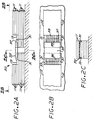
- Each step includes a forward edge 13a and side edges, and grooves 31 are formed in each of the side edges of the inwardly facing steps of the unitized circuit structures 20.
- the multilayer circuit structures 20 can have recesses similar to the recesses 15 shown in FIGS. 1A and 1B for attachment thereof to a base of a higher level assembly as described above relative to the structures 10 of FIGS. 1A and 1B.
- Metal traces 33 are disposed on the inwardly facing steps 13, and a tape 37 having metal traces 39 formed thereon spans the inwardly facing steps 13.
- a carrier element 35 is attached to the tape 37, and functions to laterally align the metal traces 39 on the tape 37 with respective metal traces 33 on the inwardly facing steps such that metal traces 39 on the tape 37 can be appropriately electrically connected to metal traces 33 on the inwardly facing steps 13, for example by soldering.
- the carrier 35 and the tape 37 attached thereto are placed on the inwardly facing steps 13 with the downwardly extending edges of the carrier engaged in the grooves 31, the metal traces 39 are laterally aligned with corresponding metal traces 33 on the inwardly facing steps 13.
- the steps 13 are formed by utilizing shorter ceramic tape layers for the layers that are above the steps while the grooves are formed by cutting or punching openings along corresponding edges of the ceramic tape layers in which the grooves are to be formed.
Landscapes
- Engineering & Computer Science (AREA)
- Microelectronics & Electronic Packaging (AREA)
- Production Of Multi-Layered Print Wiring Board (AREA)
- Combinations Of Printed Boards (AREA)
- Structure Of Printed Boards (AREA)
Applications Claiming Priority (2)
| Application Number | Priority Date | Filing Date | Title |
|---|---|---|---|
| US08/296,392 US5498905A (en) | 1994-08-26 | 1994-08-26 | Layered features for co-fired module integration |
| US296392 | 1994-08-26 |
Publications (3)
| Publication Number | Publication Date |
|---|---|
| EP0698921A2 true EP0698921A2 (fr) | 1996-02-28 |
| EP0698921A3 EP0698921A3 (fr) | 1996-10-23 |
| EP0698921B1 EP0698921B1 (fr) | 2001-04-11 |
Family
ID=23141825
Family Applications (1)
| Application Number | Title | Priority Date | Filing Date |
|---|---|---|---|
| EP95113349A Expired - Lifetime EP0698921B1 (fr) | 1994-08-26 | 1995-08-25 | Ensemble consitué d'un substrat à circuit multicouches et d'une base |
Country Status (6)
| Country | Link |
|---|---|
| US (1) | US5498905A (fr) |
| EP (1) | EP0698921B1 (fr) |
| JP (1) | JP2703522B2 (fr) |
| DE (1) | DE69520624T2 (fr) |
| ES (1) | ES2155490T3 (fr) |
| IL (1) | IL115050A (fr) |
Families Citing this family (3)
| Publication number | Priority date | Publication date | Assignee | Title |
|---|---|---|---|---|
| US5994166A (en) | 1997-03-10 | 1999-11-30 | Micron Technology, Inc. | Method of constructing stacked packages |
| US6738600B1 (en) | 2000-08-04 | 2004-05-18 | Harris Corporation | Ceramic microelectromechanical structure |
| US6437981B1 (en) | 2000-11-30 | 2002-08-20 | Harris Corporation | Thermally enhanced microcircuit package and method of forming same |
Family Cites Families (18)
| Publication number | Priority date | Publication date | Assignee | Title |
|---|---|---|---|---|
| DE2449739A1 (de) * | 1974-10-19 | 1976-04-29 | Junghans Gmbh Geb | Kontaktanordnung fuer eine auswechselbare elektronische baueinheit |
| JPS63155648A (ja) * | 1986-12-18 | 1988-06-28 | Toshiba Corp | 固体撮像素子用セラミツクパツケ−ジ |
| JPH088321B2 (ja) * | 1987-01-19 | 1996-01-29 | 住友電気工業株式会社 | 集積回路パツケ−ジ |
| US5136471A (en) * | 1987-02-26 | 1992-08-04 | Nec Corporation | Laminate wiring board |
| JPH01217950A (ja) * | 1988-02-26 | 1989-08-31 | Toshiba Corp | 固体撮像装置 |
| US4882657A (en) * | 1988-04-06 | 1989-11-21 | Ici Array Technology, Inc. | Pin grid array assembly |
| JPH02170382A (ja) * | 1988-12-23 | 1990-07-02 | Nec Corp | パッケージ実装構造 |
| JPH0322497A (ja) * | 1989-06-19 | 1991-01-30 | Toshiba Corp | セラミック多層配線基板 |
| US5399898A (en) * | 1992-07-17 | 1995-03-21 | Lsi Logic Corporation | Multi-chip semiconductor arrangements using flip chip dies |
| US5051869A (en) * | 1990-05-10 | 1991-09-24 | Rockwell International Corporation | Advanced co-fired multichip/hybrid package |
| WO1992002040A1 (fr) * | 1990-07-25 | 1992-02-06 | Dsm N.V. | Boîtier pour l'incorporation de circuits integres et procede de production associe |
| US5245216A (en) * | 1990-09-11 | 1993-09-14 | Kabushiki Kaisha Toshiba | Plastic-molded type semiconductor device |
| JP2883458B2 (ja) * | 1991-02-27 | 1999-04-19 | 株式会社東芝 | 混成集積回路用配線板の製造方法 |
| JPH0513959A (ja) * | 1991-07-02 | 1993-01-22 | Matsushita Electric Ind Co Ltd | 多層配線回路基板 |
| DE69210329T2 (de) * | 1991-07-25 | 1996-11-28 | Ncr Int Inc | Mehrschichtiger Träger für integrierte Schaltungen und Verfahren zu dessen Herstellung |
| US5397916A (en) * | 1991-12-10 | 1995-03-14 | Normington; Peter J. C. | Semiconductor device including stacked die |
| JP2903865B2 (ja) * | 1992-06-03 | 1999-06-14 | 富士通株式会社 | プリント板ユニット挿抜構造 |
| JPH06120624A (ja) * | 1992-10-08 | 1994-04-28 | Fujitsu Ltd | 微細多層配線板構造 |
-
1994
- 1994-08-26 US US08/296,392 patent/US5498905A/en not_active Expired - Fee Related
-
1995
- 1995-08-23 IL IL115050A patent/IL115050A/xx not_active IP Right Cessation
- 1995-08-25 ES ES95113349T patent/ES2155490T3/es not_active Expired - Lifetime
- 1995-08-25 EP EP95113349A patent/EP0698921B1/fr not_active Expired - Lifetime
- 1995-08-25 DE DE69520624T patent/DE69520624T2/de not_active Expired - Fee Related
- 1995-08-28 JP JP7219284A patent/JP2703522B2/ja not_active Expired - Lifetime
Non-Patent Citations (3)
| Title |
|---|
| H.T. SAWHILL ET AL.: "Low Temperature Co-Fireable Ceramics with Co-Fired Resistors", ISHM PROCEEDINGS, 1986, pages 268 - 271 |
| R.G. POND ET AL.: "Processing and Reliability of Resistors Incorporated Within Low Temperature Co-fired Ceramic Structures", ISHM PROCEEDINGS, 1986, pages 461 - 472, XP000646671 |
| W.A. VITRIOL ET AL.: "Development of a Low Temperature Co-fired Multilayer Ceramic Technology", ISHM PROCEEDINGS, 1983, pages 593 - 598 |
Also Published As
| Publication number | Publication date |
|---|---|
| JP2703522B2 (ja) | 1998-01-26 |
| DE69520624T2 (de) | 2001-08-23 |
| ES2155490T3 (es) | 2001-05-16 |
| US5498905A (en) | 1996-03-12 |
| IL115050A (en) | 1997-09-30 |
| JPH08172275A (ja) | 1996-07-02 |
| EP0698921B1 (fr) | 2001-04-11 |
| IL115050A0 (en) | 1995-12-08 |
| DE69520624D1 (de) | 2001-05-17 |
| EP0698921A3 (fr) | 1996-10-23 |
Similar Documents
| Publication | Publication Date | Title |
|---|---|---|
| US6219253B1 (en) | Molded electronic package, method of preparation using build up technology and method of shielding | |
| US5055966A (en) | Via capacitors within multi-layer, 3 dimensional structures/substrates | |
| EP0805494B1 (fr) | Module multi-couche semi-conducteur de puissance à haute densité d'empaquetage | |
| US5006673A (en) | Fabrication of pad array carriers from a universal interconnect structure | |
| US6739047B2 (en) | Method of making ceramic multilayer circuit boards mounted in a patterned metal support substrate | |
| US6760227B2 (en) | Multilayer ceramic electronic component and manufacturing method thereof | |
| US5519176A (en) | Substrate and ceramic package | |
| US4410874A (en) | Large area hybrid microcircuit assembly | |
| US4797715A (en) | Optoelectric component for surface mounting | |
| EP0713252A2 (fr) | Montage d'éléments de circuit | |
| CN100556234C (zh) | 混合型电子部件及其制造方法 | |
| EP3584833B1 (fr) | Module de puissance à alignement amélioré | |
| JPS5826826B2 (ja) | 集積回路用セラミック・パッケ−ジ | |
| US4697204A (en) | Leadless chip carrier and process for fabrication of same | |
| EP0272046A2 (fr) | Structure de circuit comprenant un substrat composite en céramique | |
| US4599486A (en) | High capacitance bus bar including multilayer ceramic capacitors | |
| EP0079211A2 (fr) | Empaquetage pour dispositif semi-conducteur et procédé pour sa fabrication | |
| KR100895964B1 (ko) | 저 프로파일 집적 모듈 상호접속들 | |
| EP0698921B1 (fr) | Ensemble consitué d'un substrat à circuit multicouches et d'une base | |
| EP1528847A1 (fr) | Insert dissipant la chaleur, circuit comprenant ledit insert et méthode de production | |
| US4568999A (en) | Multilayer ceramic capacitor on printed circuit | |
| US4630170A (en) | Decoupling capacitor and method of manufacture thereof | |
| US5429859A (en) | LTCC alignment marks for mechanical parts placement | |
| US12557673B2 (en) | Electronic circuit module | |
| EP0359513A2 (fr) | Support pour puce semi-conductrice et procédé pour sa fabrication |
Legal Events
| Date | Code | Title | Description |
|---|---|---|---|
| PUAI | Public reference made under article 153(3) epc to a published international application that has entered the european phase |
Free format text: ORIGINAL CODE: 0009012 |
|
| AK | Designated contracting states |
Kind code of ref document: A2 Designated state(s): DE ES GB |
|
| PUAL | Search report despatched |
Free format text: ORIGINAL CODE: 0009013 |
|
| AK | Designated contracting states |
Kind code of ref document: A3 Designated state(s): DE ES GB |
|
| 17P | Request for examination filed |
Effective date: 19970326 |
|
| 17Q | First examination report despatched |
Effective date: 19980616 |
|
| RAP1 | Party data changed (applicant data changed or rights of an application transferred) |
Owner name: RAYTHEON COMPANY |
|
| GRAG | Despatch of communication of intention to grant |
Free format text: ORIGINAL CODE: EPIDOS AGRA |
|
| RTI1 | Title (correction) |
Free format text: ASSEMBLY OF A MULTILAYER CIRCUIT STRUCTURE AND A BASE |
|
| GRAG | Despatch of communication of intention to grant |
Free format text: ORIGINAL CODE: EPIDOS AGRA |
|
| GRAH | Despatch of communication of intention to grant a patent |
Free format text: ORIGINAL CODE: EPIDOS IGRA |
|
| RTI1 | Title (correction) |
Free format text: ASSEMBLY OF A MULTILAYER CIRCUIT STRUCTURE AND A BASE |
|
| GRAH | Despatch of communication of intention to grant a patent |
Free format text: ORIGINAL CODE: EPIDOS IGRA |
|
| GRAA | (expected) grant |
Free format text: ORIGINAL CODE: 0009210 |
|
| AK | Designated contracting states |
Kind code of ref document: B1 Designated state(s): DE ES GB |
|
| REG | Reference to a national code |
Ref country code: ES Ref legal event code: FG2A Ref document number: 2155490 Country of ref document: ES Kind code of ref document: T3 |
|
| REF | Corresponds to: |
Ref document number: 69520624 Country of ref document: DE Date of ref document: 20010517 |
|
| REG | Reference to a national code |
Ref country code: GB Ref legal event code: IF02 |
|
| PLBE | No opposition filed within time limit |
Free format text: ORIGINAL CODE: 0009261 |
|
| STAA | Information on the status of an ep patent application or granted ep patent |
Free format text: STATUS: NO OPPOSITION FILED WITHIN TIME LIMIT |
|
| 26N | No opposition filed | ||
| PGFP | Annual fee paid to national office [announced via postgrant information from national office to epo] |
Ref country code: GB Payment date: 20020712 Year of fee payment: 8 |
|
| PGFP | Annual fee paid to national office [announced via postgrant information from national office to epo] |
Ref country code: DE Payment date: 20020724 Year of fee payment: 8 |
|
| PGFP | Annual fee paid to national office [announced via postgrant information from national office to epo] |
Ref country code: ES Payment date: 20020812 Year of fee payment: 8 |
|
| PG25 | Lapsed in a contracting state [announced via postgrant information from national office to epo] |
Ref country code: GB Free format text: LAPSE BECAUSE OF NON-PAYMENT OF DUE FEES Effective date: 20030825 |
|
| PG25 | Lapsed in a contracting state [announced via postgrant information from national office to epo] |
Ref country code: ES Free format text: LAPSE BECAUSE OF NON-PAYMENT OF DUE FEES Effective date: 20030826 |
|
| PG25 | Lapsed in a contracting state [announced via postgrant information from national office to epo] |
Ref country code: DE Free format text: LAPSE BECAUSE OF NON-PAYMENT OF DUE FEES Effective date: 20040302 |
|
| GBPC | Gb: european patent ceased through non-payment of renewal fee | ||
| REG | Reference to a national code |
Ref country code: ES Ref legal event code: FD2A Effective date: 20030826 |