EP0698979A2 - Circuit de commande en courant pour bus différentiel - Google Patents
Circuit de commande en courant pour bus différentiel Download PDFInfo
- Publication number
- EP0698979A2 EP0698979A2 EP95305038A EP95305038A EP0698979A2 EP 0698979 A2 EP0698979 A2 EP 0698979A2 EP 95305038 A EP95305038 A EP 95305038A EP 95305038 A EP95305038 A EP 95305038A EP 0698979 A2 EP0698979 A2 EP 0698979A2
- Authority
- EP
- European Patent Office
- Prior art keywords
- source
- current
- drain
- mosfet
- electrode
- Prior art date
- Legal status (The legal status is an assumption and is not a legal conclusion. Google has not performed a legal analysis and makes no representation as to the accuracy of the status listed.)
- Withdrawn
Links
- 239000000872 buffer Substances 0.000 claims abstract description 11
- 230000004044 response Effects 0.000 claims abstract description 5
- 230000008878 coupling Effects 0.000 claims description 18
- 238000010168 coupling process Methods 0.000 claims description 18
- 238000005859 coupling reaction Methods 0.000 claims description 18
- 229910044991 metal oxide Inorganic materials 0.000 claims description 6
- 150000004706 metal oxides Chemical class 0.000 claims description 6
- 239000004065 semiconductor Substances 0.000 claims description 6
- 230000000295 complement effect Effects 0.000 claims description 3
- 230000005669 field effect Effects 0.000 claims description 3
- 238000010586 diagram Methods 0.000 description 6
- 238000002955 isolation Methods 0.000 description 5
- 230000005540 biological transmission Effects 0.000 description 2
- 238000013459 approach Methods 0.000 description 1
- 238000005516 engineering process Methods 0.000 description 1
- 230000036039 immunity Effects 0.000 description 1
- 238000000034 method Methods 0.000 description 1
- 230000008569 process Effects 0.000 description 1
- 230000001052 transient effect Effects 0.000 description 1
- 230000007704 transition Effects 0.000 description 1
Images


Classifications
-
- H—ELECTRICITY
- H03—ELECTRONIC CIRCUITRY
- H03K—PULSE TECHNIQUE
- H03K17/00—Electronic switching or gating, i.e. not by contact-making and –breaking
- H03K17/04—Modifications for accelerating switching
- H03K17/041—Modifications for accelerating switching without feedback from the output circuit to the control circuit
- H03K17/04106—Modifications for accelerating switching without feedback from the output circuit to the control circuit in field-effect transistor switches
Definitions
- This invention relates to circuits that can be used to drive differential backplane buses and more particularly to circuits which drive these buses in a way such that the difference in voltage on the bus represents a digital binary value.
- a typical prior art differential bus for ECL (emitter coupled logic) consists of differential leads that must be isolated from the bus when a master is not using the bus. ECL achieves this isolation by using a third output state of the driver which is a high impedance isolation state.
- ECL emitter coupled logic
- both signal paths are biased equally to an appropriate ECL termination voltage which is normally 2 volts below the top rail voltage.
- ECL termination voltage which is normally 2 volts below the top rail voltage.
- ECL Error-Coupled C
- Still another difficulty with commonly used interface technologies is that they use voltage mode bus drivers which drive the bus to certain predetermined voltages to represent the logic states.
- the time slot period for one bit approaches the amount of time that a signal edge takes to traverse a fraction of the backplane length.
- the last digital bit from one of the masters can be passing a second master on the bus when it is time for that second master to begin transmission. If the second master sees the digital value on the bus which it intends to transmit, the voltage mode bus driver from that second master will not contribute to the bus until that last bit from the first master is ended. This causes the bus driver in the second master to produce a first digital bit with less than the full time slot period, and this short digital bit typically cannot be properly received.
- a backplane bus for differential signals is provided wherein two signal leads are present for each of the digital bits to be transmitted on the bus.
- the two signal leads for each one of the digital bits are terminated with their characteristic impedances by a network at each end of the transmission paths, and these networks bias the two signal leads with a different DC voltage on each one of the two leads.
- This normally present DC voltage difference between the two leads represents one of the two binary digital states.
- Digital information is coupled to the two leads of the bus for each digital bit through a current mode bus driver which couples current into one of the two leads and out of the other one of the two leads in response to the other binary digital state, thereby changing the difference in voltage between the two leads.
- the current mode bus driver for this new advantageous bus must be isolated from the bus for one of the two binary digital states and must couple current into one of the two leads of the bus and out of the other one of the two leads of the bus for the other one of the two binary digital states.
- the present invention involves a current mode bus driver which is useful in coupling an input digital signal to a differential voltage bus of the type which is biased with a voltage difference representing one binary type.
- a current source is connected to one lead of the bus and a current sink is connected to the other lead of the bus when the input digital signal represents the other binary type, thereby changing the voltage difference on the bus to represent that other binary type.
- the current source and are current sink are connected together and isolated from the bus.
- the current source and current sink are switchably connected together or to the bus by MOSFETs whose gates are driven by unique buffer driver circuits each of which uses an NPN transistor to drive the gate of a MOSFET with a high peak current thereby ensuring rapid switching of voltages on the bus.
- the current source and current sink are provided by a unique combination of MOSFETs and NPN transistors thereby permitting the differential voltages on the bus to swing around a lower voltage than would otherwise be permitted.
- FIG. 1 A current mode bus driver of the type useful in coupling pseudo or positive emitter coupled logic (PECL) signals to the DL backplane bus disclosed in my above-identified copending application is shown in Fig. 1.
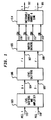
- the circuits of figures 2, 3, 4 and 5 are connected in tandem as shown to provide an apparatus which causes the PECL differential voltage signals to operate the signal leads L+ and L- of the BUS. The operation of the entire apparatus will be more readily understood after reading the following detailed description of the operation of the individual circuits of Figs. 2-5.
- the essential characteristic of the current mode bus driver of Fig. 1 is to supply a current source to one signal lead of the bus and a current sink to the other signal lead of the bus for an input binary value of one type, and to isolate the current source and sink from the bus for an input binary value of the other type.
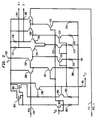
- the part of the apparatus in Fig. 1 which accomplishes this task is present in the circuit of Fig. 5, and it is therefore most useful in obtaining an understanding of the present invention to discuss this circuit first.
- the remaining circuits of Figs. 2-4 simply modify the voltage levels of the PECL signals at the input of the apparatus and increase their power level to the point where they can effectively switch the current source and sink at a high rate of speed with digital signals on lines 110-113 at the input of block 114 in Fig. 1.
- a fixed reference potential, V cs is coupled to the base of an NPN transistor 501 whose emitter is connected through a resistor 502 to ground thereby establishing a reference current into the collector of transistor 501.
- the collector of transistor 501 is connected to, and the reference current is drawn from, the drain of a metal oxide semiconductor field effect transistor (MOSFET) 503 of the p-channel enhancement type.
- MOSFET metal oxide semiconductor field effect transistor
- the gate of MOSFET 503 is also connected to its drain, and its source electrode is connected to a potential source 515 of V s , which in the present embodiment is equal to 5 volts.
- a MOSFET 504 of the p-channel enhancement type also has its source electrode connected to the potential source of V s , and has its gate electrode connected to the gate electrode of MOSFET 503.
- MOSFET's 503 and 504 are connected in a current mirror arrangement whereby the current out of the drain of MOSFET 504 is related to the current out of the drain of MOSFET 503 by the ratio of the widths of the gate electrodes. Since the current out of the drain of MOSFET 503 is only used as a reference current, it is set, by choosing the value of resistor 502, equal to about one-fourth the current out of the drain of MOSFET 504 in order to reduce the amount of power consumed. In the present embodiment, the desired current is equal to about 10 ma., and the reference current is equal to about 2.5 ma. Accordingly, the width of the gate electrode of MOSFET 504 is chosen to be equal to four times the width of the gate electrode of MOSFET 503.
- a MOSFET 508 of the p-channel enhancement type also has its source electrode connected to the potential source, V s , and its gate electrode connected to the gate electrode of MOSFET 503 with a gate electrode width equal to that of MOSFET 504.
- V s potential source
- MOSFET 503 MOSFET 503 with a gate electrode width equal to that of MOSFET 504.
- a mirrored current of about 10 ma. is available from the drain of MOSFET 508 on line 516. This is the current which in selected cases will be switched in a manner to be described hereinafter onto signal lead 102 (L+) of the BUS.
- the mirrored current out of the drain of MOSFET 504 is coupled into the collector electrode of an NPN transistor 505.
- the collector of transistor 505 is connected to its base electrode through the base-emitter junction of an NPN transistor 507, the collector electrode of which is connected to the potential source 515 of V s .
- the emitter of transistor 505 is connected through a resistor 506 to ground.
- An NPN transistor 509 with an emitter area equal to that of transistor 505 has its base electrode connected to the base of transistor 505, and its emitter electrode connected to ground through a resistor 510 substantially equal in value to resistor 506.
- transistors 505, 507 and 509 as a current mirror which provides a current sink at the collector of transistor 509 for a current, I-, on line 517 equal in value to the current being driven into the collector of transistor 505.
- this current into the collector of transistor 505 is equal in value to the current, I+, on line 516, and therefor the magnitude of current source of I+ is substantially equal to the magnitude current sink of I-.
- the current, I+, on line 516 is connected to the drain of an n-channel enhancement type MOSFET 510 whose source is connected to signal lead 102 (L+) and whose gate is connected to receive a digital signal (COH) present on line 110.
- the current, I+ is coupled through to signal lead 102 (L+) of the BUS.
- the current, I-, on line 517 is connected to the source of an n-channel enhancement type MOSFET 511 whose drain is connected to signal lead 101 (L-) of the BUS and whose gate is connected to receive a digital signal (COL) on line 111.
- signal lead 101 (L-) of the BUS is connected through to the current sink, I-, on line 517.
- the current, I+, on line 516 is also connected to the drain of a n-channel enhancement type MOSFET 512 whose gate is connected to receive a digital signal (CBH) on a line 112.
- the source of MOSFET 512 is directly connected to the drain of an n-channel enhancement type MOSFET 513 whose gate is connected to receive a digital signal (CBL) on line 113 and whose source is connected to the current sink, I-, on line 517.
- CBH digital signal
- CBL digital signal
- the current source and current sink can be rapidly switched between the signal leads of the BUS and isolated from the BUS without introducing large transient effects. Consequently, the circuit of Fig. 5 can be driven by signals from any other type logic system such as ECL or PECL by translating the signals from that other logic system into signals on lines 110-113 with the correct polarity and sufficient power to operate the switches represented by MOSFET's 510-513.
- the circuit of Fig. 4 has four novel buffers which can advantageously provide this high peak current on lines 110-113 in response to two digital input signals F+ and F- on lines 107 and 108 respectively.
- lines 110-113 are each connected to the emitter of an NPN transistor 400-403 respectively.
- the collector electrodes of these transistors 400-403 are all connected to the positive potential source 515 of V s .
- P-channel enhancement type MOSFET's 410-413 are connected with n-channel enhancement type MOSFETs 420-423 to form four standard complementary metal oxide semiconductor (CMOS) inverters.
- CMOS complementary metal oxide semiconductor
- each of the NPN transistors is connected to the output of one of these inverters. Consequently, if the gate of any one of the MOSFETs 410-413 is driven with a sufficiently low voltage relative to the positive potential source, V s , the MOSFET drives its respective NPN transistor toward conduction and the corresponding MOSFET switch in Fig. 5 is closed. As shown in Fig. 4, MOSFET's 410 and 411 are driven by the F- signal on line 108 whereas MOSFET's 412 and 413 are driven by the F+ signal on line 107.
- each F signal has a voltage transition of about 2.0 volts centered about 2.5 volts, that is, each F signal swings between 1.5 and 3.5 volts.
- the corresponding p-channel MOSFET (410-413) passes so little current that the corresponding NPN transistor is no longer able to conduct since the corresponding n-channel MOSFET (420-423) is driven toward saturation by the 3.5 volts thereby effectively removing current which would otherwise flow into the base electrode of the corresponding NPN transistor.
- n-channel enhancement type MOSFET's 430-433 each has its drain electrode connected to one of the lines 110-113 respectively, and its source connected to ground.
- the gate of each of the MOSFET's 430-433 is connected to the F signal driving its respective switch in Fig. 5. Consequently, when the F- signal on line 108 is driven to the 3.5 volt level, MOSFET's 430 and 431 are driven toward saturation thereby causing MOSFET switches 510 and 511 in Fig. 5 to be turned off.
- MOSFET's 432 and 433 are driven toward saturation thereby causing MOSFET switches 512 and 513 in Fig. 5 to be turned off.
- the low level of 1.5 volt for the F-signal on line 108 causes the circuit of Fig. 5 to connect the current source and sink to the signal lines 102 and 101 of the BUS
- the low level of 1.5 volt for the F+ signal on line 107 causes the current source and sink to be connected together and isolated from the BUS.
- the high level signal of 3.5 volt on either of the F signals causes its corresponding MOSFET switch to be rapidly turned off.
- differential voltage digital signals represented by F+ and F- on lines 107 and 108 respectively can be used to drive a DL bus of the type disclosed in my above-identified copending application.
- the F signals have a 2.0 volt swing around a median value of about 2.5 volts.
- Those skilled in the art can use this information to design circuits which can translate any one of the well known digital formats into F signals that can be used to drive the Figs. 4 and 5 apparatus.
- the present embodiment shown in Fig 1 uses input signals on lines 115 and 116 from a positive or pseudo ECL (PECL) system. Each PECL signal has a swing of about 0.8 volts around a median voltage of about 3.6 volts.
- the function of the remainder of the circuits shown in Figs. 2 and 3 is to translate the input PECL signals into F signals on lines 107 and 108 which can properly drive the buffer driver circuits of Fig. 4.
- the fixed reference potential (V CS ) of about 1.8 volts is connected to the base of an NPN transistor 201.
- the emitter of transistor 201 is connected through a resistor 202 to ground and its collector is connected to the drain of a p-channel enhancement type MOSFET 203.
- MOSFET 203 is connected with a p-channel enhancement type MOSFET 204 in a current mirror arrangement which functions in a fashion identical to that of the current mirror arrangement discussed herein above in connection with MOSFET's 503 and 504.
- the reference current established into the collector of transistor 201 is mirrored out of the drain of MOSFET 204, and this mirrored current is coupled into the collector of an NPN transistor 205 which in turn is connected with transistor 206 and resistor 225 in an arrangement which functions in a fashion identical to that described herein above with respect to elements 505-507 in Fig. 5.
- a reference potential, V LS is established at the base of transistor 205.
- the fixed reference potential, V CS is also connected to the base electrodes of transistors 207 and 223 each of which has its emitter electrode connected through a resistor (208 and 224 respectively) to ground.
- the current into the collector of transistor 207 is drawn from the emitter of an NPN transistor 209 whose collector is connected to the 5.0 volt potential source 515 and whose base is connected to line 116 to receive the PECL- signal.
- the emitter follower stage formed by transistor 209 simply drops the PECL- signal by about 1 volt.
- an NPN transistor 219 provides an emitter follower stage with the current into the collector of transistor 223 to receive and drop the potential of the PECL+ signal on line 115.
- the reference potential of V LS on the base of transistor 205 is coupled to the bases of NPN transistors 211, 213, and 221 each of which has its emitter electrode connected through resistors 212, 214 and 222, respectively, to ground thereby forming three more current sinks into their collector electrodes.
- the NPN transistors 210 and 220 are connected to two of these current sinks to form two additional emitter followers that serve to drop the PECL- and PECL+ signals out of the first emitter follower stages by an additional volt.
- the resulting digital signals at the emitters of transistors 210 and 220 are now centered around a potential of about 1.6 volts as compared with the 3.6 volt of the original PECL signals.
- the current into the collector of transistor 213 is drawn from the emitter electrodes of NPN transistors 215 and 216 each of which has its collector electrode connected through a resistor 217 and 218 respectively to form a differential amplifier stage.
- This differential amplifier stage has its inputs (bases of transistors 215 and 216) connected to receive the signals at the emitters of transistors 210 and 220.
- the amplified signals are the D+ and D- signals provided on the lines 104 and 105 in Fig. 1. These amplified D signals have about a 2 volt swing centered around about 3.5 volts.
- the reference potential of V LS from Fig. 2 is connected by way of line 301 to the base electrodes of NPN transistors 302 and 304 each of which has its emitter electrode connected through a resistor 303 and 305, respectively, to ground.
- the resulting current sinks into the collectors of transistors 302 and 304 are drawn from the emitters of NPN transistors 306 and 307 each of which has its collector electrode connected to positive potential source 515 in order to form two additional emitter follower stages.
- the D+ and D- signals on lines 104 and 105 are coupled to the base electrodes of transistors 306 and 307 respectively.
Landscapes
- Logic Circuits (AREA)
Applications Claiming Priority (2)
| Application Number | Priority Date | Filing Date | Title |
|---|---|---|---|
| US281057 | 1994-07-27 | ||
| US08/281,057 US5450026A (en) | 1994-07-27 | 1994-07-27 | Current mode driver for differential bus |
Publications (2)
| Publication Number | Publication Date |
|---|---|
| EP0698979A2 true EP0698979A2 (fr) | 1996-02-28 |
| EP0698979A3 EP0698979A3 (fr) | 1996-04-24 |
Family
ID=23075769
Family Applications (1)
| Application Number | Title | Priority Date | Filing Date |
|---|---|---|---|
| EP95305038A Withdrawn EP0698979A3 (fr) | 1994-07-27 | 1995-07-19 | Circuit de commande en courant pour bus différentiel |
Country Status (4)
| Country | Link |
|---|---|
| US (1) | US5450026A (fr) |
| EP (1) | EP0698979A3 (fr) |
| JP (1) | JPH0876901A (fr) |
| CA (1) | CA2152109A1 (fr) |
Families Citing this family (26)
| Publication number | Priority date | Publication date | Assignee | Title |
|---|---|---|---|---|
| JP3640703B2 (ja) * | 1995-05-24 | 2005-04-20 | 株式会社ルネサステクノロジ | バス駆動回路、レシーバ回路およびバスシステム |
| US5699013A (en) * | 1995-12-11 | 1997-12-16 | Thomson Consumer Electronics, Inc. | Tri-state audio differential driver |
| US5880689A (en) * | 1995-12-11 | 1999-03-09 | Massachusetts Institute Of Technology | Balanced digital-to-analog converter |
| US5767699A (en) * | 1996-05-28 | 1998-06-16 | Sun Microsystems, Inc. | Fully complementary differential output driver for high speed digital communications |
| US5959481A (en) * | 1997-02-18 | 1999-09-28 | Rambus Inc. | Bus driver circuit including a slew rate indicator circuit having a one shot circuit |
| US5889430A (en) * | 1997-06-26 | 1999-03-30 | The Aerospace Corporation | Current mode transistor circuit |
| US5889431A (en) * | 1997-06-26 | 1999-03-30 | The Aerospace Corporation | Current mode transistor circuit method |
| DE19803796B4 (de) * | 1998-01-30 | 2006-10-26 | Telefonaktiebolaget Lm Ericsson (Publ) | Ausgangspuffer zum Ansteuern einer symmetrischen Übertragungsleitung |
| US6184714B1 (en) | 1998-02-25 | 2001-02-06 | Vanguard International Semiconductor Corporation | Multiple-bit, current mode data bus |
| US6194949B1 (en) * | 1998-03-04 | 2001-02-27 | Nortel Networks Limited | Driver circuit for high speed data |
| KR100307634B1 (ko) | 1998-11-04 | 2001-11-07 | 윤종용 | 전류제어 회로 및 이를 구비하는 패킷 방식 반도체 메모리장치 |
| US6255852B1 (en) | 1999-02-09 | 2001-07-03 | Micron Technology, Inc. | Current mode signal interconnects and CMOS amplifier |
| US7554829B2 (en) | 1999-07-30 | 2009-06-30 | Micron Technology, Inc. | Transmission lines for CMOS integrated circuits |
| JP3498042B2 (ja) * | 2000-06-05 | 2004-02-16 | Necエレクトロニクス株式会社 | 電子機器及びそれを備えた電子機器システム |
| US6476642B1 (en) | 2000-07-17 | 2002-11-05 | Agere Systems Guardian Corp. | Differential current driver circuit |
| US7101770B2 (en) | 2002-01-30 | 2006-09-05 | Micron Technology, Inc. | Capacitive techniques to reduce noise in high speed interconnections |
| US7235457B2 (en) | 2002-03-13 | 2007-06-26 | Micron Technology, Inc. | High permeability layered films to reduce noise in high speed interconnects |
| US6900116B2 (en) | 2002-03-13 | 2005-05-31 | Micron Technology Inc. | High permeability thin films and patterned thin films to reduce noise in high speed interconnections |
| US6846738B2 (en) * | 2002-03-13 | 2005-01-25 | Micron Technology, Inc. | High permeability composite films to reduce noise in high speed interconnects |
| US7160577B2 (en) | 2002-05-02 | 2007-01-09 | Micron Technology, Inc. | Methods for atomic-layer deposition of aluminum oxides in integrated circuits |
| US7192892B2 (en) | 2003-03-04 | 2007-03-20 | Micron Technology, Inc. | Atomic layer deposited dielectric layers |
| US6970053B2 (en) * | 2003-05-22 | 2005-11-29 | Micron Technology, Inc. | Atomic layer deposition (ALD) high permeability layered magnetic films to reduce noise in high speed interconnection |
| US7927948B2 (en) | 2005-07-20 | 2011-04-19 | Micron Technology, Inc. | Devices with nanocrystals and methods of formation |
| US7631953B2 (en) * | 2006-03-31 | 2009-12-15 | Lexmark International, Inc. | Micro-fluid ejection apparatus signal communication devices and methods |
| US11462283B2 (en) * | 2020-08-26 | 2022-10-04 | Micron Technology, Inc. | Latch circuits with improved single event upset immunity and related systems, apparatuses, and methods |
| CN121309257B (zh) * | 2025-12-11 | 2026-04-17 | 盈力半导体(上海)有限公司 | 总线驱动电路和通信接口 |
Family Cites Families (7)
| Publication number | Priority date | Publication date | Assignee | Title |
|---|---|---|---|---|
| DE1933052A1 (de) * | 1969-06-30 | 1971-01-07 | Licentia Gmbh | Anordnung zur Datenuebertragung |
| JPS63240109A (ja) * | 1987-03-27 | 1988-10-05 | Toshiba Corp | 差動増幅器 |
| GB2209104A (en) * | 1987-08-26 | 1989-04-26 | Philips Nv | An amplifier load circuit and an amplifier including the load circuit |
| US4890010A (en) * | 1988-12-22 | 1989-12-26 | Ncr Corporation | Matched current source serial bus driver |
| GB8912461D0 (en) * | 1989-05-31 | 1989-07-19 | Lucas Ind Plc | Line driver |
| JP2545146B2 (ja) * | 1990-01-25 | 1996-10-16 | 富士通株式会社 | レベル変換回路 |
| US5146111A (en) * | 1991-04-10 | 1992-09-08 | International Business Machines Corporation | Glitch-proof powered-down on chip receiver with non-overlapping outputs |
-
1994
- 1994-07-27 US US08/281,057 patent/US5450026A/en not_active Expired - Lifetime
-
1995
- 1995-06-19 CA CA002152109A patent/CA2152109A1/fr not_active Abandoned
- 1995-07-19 EP EP95305038A patent/EP0698979A3/fr not_active Withdrawn
- 1995-07-26 JP JP7209323A patent/JPH0876901A/ja active Pending
Non-Patent Citations (1)
| Title |
|---|
| None |
Also Published As
| Publication number | Publication date |
|---|---|
| EP0698979A3 (fr) | 1996-04-24 |
| US5450026A (en) | 1995-09-12 |
| JPH0876901A (ja) | 1996-03-22 |
| CA2152109A1 (fr) | 1996-01-28 |
Similar Documents
| Publication | Publication Date | Title |
|---|---|---|
| US5450026A (en) | Current mode driver for differential bus | |
| EP1316146B1 (fr) | Circuit permettant de produire des signaux differentiels basse tension | |
| JP4215134B2 (ja) | 対称な差分出力信号を持つcanバスドライバ | |
| KR100324987B1 (ko) | 차동트라이스테이트 발생방법 및 차동트라이스테이트 회로 | |
| JP2002094365A (ja) | 出力バッファ回路 | |
| JP2975122B2 (ja) | レベル変換回路 | |
| US5430396A (en) | Backplane bus for differential signals | |
| US5097148A (en) | Integrated circuit buffer with improved drive capability | |
| AU717718B2 (en) | Universal sender device | |
| JPH06224733A (ja) | 送受信回路およびそのための方法 | |
| CN103312312A (zh) | 半导体器件 | |
| JPH07321636A (ja) | 電流スイッチング回路 | |
| JP3509900B2 (ja) | 出力バッファ回路と入力バッファ回路とを有するシステム | |
| US6239619B1 (en) | Method and apparatus for dynamic termination logic of data buses | |
| JP2001257578A (ja) | ドライバ回路 | |
| US5982191A (en) | Broadly distributed termination for buses using switched terminator logic | |
| US5869984A (en) | Output buffer circuit utilizing FETS for lowering output resistance of a circuit block | |
| EP0490243A1 (fr) | Circuit d'attaque de sortie à trois états BICMOS | |
| JPH10126316A (ja) | 終端装置 | |
| WO1996003738A1 (fr) | Procede pour multiplexer des informations video | |
| US20040119498A1 (en) | Converter from ECL to CMOS and network element for transmitting signals | |
| JP2998329B2 (ja) | 半導体集積回路 | |
| JP2903885B2 (ja) | Cmos出力バッファ回路 | |
| JPH0422313Y2 (fr) | ||
| JPH1022808A (ja) | 信号伝送回路 |
Legal Events
| Date | Code | Title | Description |
|---|---|---|---|
| PUAI | Public reference made under article 153(3) epc to a published international application that has entered the european phase |
Free format text: ORIGINAL CODE: 0009012 |
|
| AK | Designated contracting states |
Kind code of ref document: A2 Designated state(s): DE ES FR GB IT |
|
| PUAL | Search report despatched |
Free format text: ORIGINAL CODE: 0009013 |
|
| AK | Designated contracting states |
Kind code of ref document: A3 Designated state(s): DE ES FR GB IT |
|
| 17P | Request for examination filed |
Effective date: 19961010 |
|
| 17Q | First examination report despatched |
Effective date: 20001229 |
|
| STAA | Information on the status of an ep patent application or granted ep patent |
Free format text: STATUS: THE APPLICATION IS DEEMED TO BE WITHDRAWN |
|
| 18D | Application deemed to be withdrawn |
Effective date: 20010509 |