EP0700086A2 - Boîtier de circuit intégré avec dissipation de chaleur améliorée - Google Patents
Boîtier de circuit intégré avec dissipation de chaleur améliorée Download PDFInfo
- Publication number
- EP0700086A2 EP0700086A2 EP95305611A EP95305611A EP0700086A2 EP 0700086 A2 EP0700086 A2 EP 0700086A2 EP 95305611 A EP95305611 A EP 95305611A EP 95305611 A EP95305611 A EP 95305611A EP 0700086 A2 EP0700086 A2 EP 0700086A2
- Authority
- EP
- European Patent Office
- Prior art keywords
- leadframe
- package
- lead portions
- inner lead
- leads
- Prior art date
- Legal status (The legal status is an assumption and is not a legal conclusion. Google has not performed a legal analysis and makes no representation as to the accuracy of the status listed.)
- Withdrawn
Links
Images


Classifications
-
- H—ELECTRICITY
- H10—SEMICONDUCTOR DEVICES; ELECTRIC SOLID-STATE DEVICES NOT OTHERWISE PROVIDED FOR
- H10W—GENERIC PACKAGES, INTERCONNECTIONS, CONNECTORS OR OTHER CONSTRUCTIONAL DETAILS OF DEVICES COVERED BY CLASS H10
- H10W70/00—Package substrates; Interposers; Redistribution layers [RDL]
- H10W70/40—Leadframes
- H10W70/411—Chip-supporting parts, e.g. die pads
- H10W70/415—Leadframe inner leads serving as die pads
-
- H—ELECTRICITY
- H10—SEMICONDUCTOR DEVICES; ELECTRIC SOLID-STATE DEVICES NOT OTHERWISE PROVIDED FOR
- H10W—GENERIC PACKAGES, INTERCONNECTIONS, CONNECTORS OR OTHER CONSTRUCTIONAL DETAILS OF DEVICES COVERED BY CLASS H10
- H10W70/00—Package substrates; Interposers; Redistribution layers [RDL]
- H10W70/40—Leadframes
- H10W70/461—Leadframes specially adapted for cooling
-
- H—ELECTRICITY
- H10—SEMICONDUCTOR DEVICES; ELECTRIC SOLID-STATE DEVICES NOT OTHERWISE PROVIDED FOR
- H10W—GENERIC PACKAGES, INTERCONNECTIONS, CONNECTORS OR OTHER CONSTRUCTIONAL DETAILS OF DEVICES COVERED BY CLASS H10
- H10W72/00—Interconnections or connectors in packages
- H10W72/50—Bond wires
- H10W72/541—Dispositions of bond wires
- H10W72/5449—Dispositions of bond wires not being orthogonal to a side surface of the chip, e.g. fan-out arrangements
-
- H—ELECTRICITY
- H10—SEMICONDUCTOR DEVICES; ELECTRIC SOLID-STATE DEVICES NOT OTHERWISE PROVIDED FOR
- H10W—GENERIC PACKAGES, INTERCONNECTIONS, CONNECTORS OR OTHER CONSTRUCTIONAL DETAILS OF DEVICES COVERED BY CLASS H10
- H10W72/00—Interconnections or connectors in packages
- H10W72/851—Dispositions of multiple connectors or interconnections
- H10W72/874—On different surfaces
- H10W72/884—Die-attach connectors and bond wires
-
- H—ELECTRICITY
- H10—SEMICONDUCTOR DEVICES; ELECTRIC SOLID-STATE DEVICES NOT OTHERWISE PROVIDED FOR
- H10W—GENERIC PACKAGES, INTERCONNECTIONS, CONNECTORS OR OTHER CONSTRUCTIONAL DETAILS OF DEVICES COVERED BY CLASS H10
- H10W74/00—Encapsulations, e.g. protective coatings
-
- H—ELECTRICITY
- H10—SEMICONDUCTOR DEVICES; ELECTRIC SOLID-STATE DEVICES NOT OTHERWISE PROVIDED FOR
- H10W—GENERIC PACKAGES, INTERCONNECTIONS, CONNECTORS OR OTHER CONSTRUCTIONAL DETAILS OF DEVICES COVERED BY CLASS H10
- H10W90/00—Package configurations
- H10W90/701—Package configurations characterised by the relative positions of pads or connectors relative to package parts
- H10W90/731—Package configurations characterised by the relative positions of pads or connectors relative to package parts of die-attach connectors
- H10W90/736—Package configurations characterised by the relative positions of pads or connectors relative to package parts of die-attach connectors between a chip and a stacked lead frame, conducting package substrate or heat sink
-
- H—ELECTRICITY
- H10—SEMICONDUCTOR DEVICES; ELECTRIC SOLID-STATE DEVICES NOT OTHERWISE PROVIDED FOR
- H10W—GENERIC PACKAGES, INTERCONNECTIONS, CONNECTORS OR OTHER CONSTRUCTIONAL DETAILS OF DEVICES COVERED BY CLASS H10
- H10W90/00—Package configurations
- H10W90/701—Package configurations characterised by the relative positions of pads or connectors relative to package parts
- H10W90/751—Package configurations characterised by the relative positions of pads or connectors relative to package parts of bond wires
- H10W90/756—Package configurations characterised by the relative positions of pads or connectors relative to package parts of bond wires between a chip and a stacked lead frame, conducting package substrate or heat sink
Definitions
- the present invention relates to the housing and protection of integrated circuit chips. More specifically, the present invention relates to a leadframe structure that offers enhanced thermal dissipation for integrated circuit chips.
- the leadframe typically consists of a metallic paddle on which the IC is mounted and lead fingers for providing electrically conductive paths from the bonding pads of the IC to external elements, such as circuit boards.
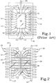
- FIG. 1 An example of a prior leadframe is illustrated in FIG. 1.
- the IC 10 is typically attached to a leadframe paddle 12 .
- Electrically conductive lead fingers 14 are electrically connected to the IC 10 with wire bonds 16 and serve to provide electrically conductive paths from the IC 10 to external elements (not shown).
- the leadframe is typically encapsulated in a moulding compound 18 .
- the external widths of the lead fingers 14 are typically standardized according to the type of package. For example, 8-lead dual in-line plastic (DIP) and 8-lead small outline integrated circuit (SOIC) packages have outer lead finger portions that are between approximately 0.33 and 0.51 mm wide.
- DIP dual in-line plastic
- SOIC small outline integrated circuit
- the heat conduction paths are along extensions 20 of the leadframe paddle 12 and through the moulding compound 18 , which typically has poor thermal conductivity when compared to the lead fingers (which are typically made of copper). Although the lead fingers 14 are generally excellent heat conductors,they contribute relatively little to the thermal dissipation because the distance and moulding compound between them and the paddle 12 lowers the thermal conductivity.
- the size of the IC 10 that this type of leadframe can accomodate is limited by the size of the leadframe paddle 12 .
- the package dimensions In order to incorporate the Bayan design into standard package designs, such as 8-lead DIP or 8-lead SOIC packages, the package dimensions must be increased by up to 50 percent to accommodate the additional paddle pins. As a result, these packages must be redesigned to accommodate the Bayan leadframe structure.
- Another leadframe structure increases thermal dissipation by placing the inner ends of the lead fingers in close proximity to the leadframe paddle and branching the outer ends of each lead finger, so that a portion of each lead finger is attached to a thermally conductive sheet positioned on top of the IC package.
- the Sasahara structure improves thermal dissipation over standard leadframe structures, additional tooling is required to trim and form the lead fingers after the leadframe has been encapsulated in the moulding compound, and additional manufacturing steps are required to apply the thermally conductive sheet to the top of the IC package.
- a third leadframe structure described in United States Patent No. 4,943,843 by Okinaga et al., extends some of the lead fingers underneath the IC so that they are better anchored to the moulding compound that typically encapsulates the leadframe and IC.
- a side benefit of this design is increased thermal dissipation via the lead fingers that extend underneath the IC. However, an even higher level of heat transfer is desirable.
- the present invention provides a leadframe that exhibits high thermal dissipation and that can be incorporated in standard IC package designs.
- High thermal dissipation is achieved by widening the inner lead portions with respect to the outer lead portions and extending them along a major surface of the IC.
- the wide inner lead portions cover at least 80 percent of the IC surface and also support the IC, eliminating the need for a leadframe paddle.
- the wide inner lead portions are more efficient in conducting heat away from the IC than prior "standard" width inner lead portions because of the increased thermal contact area between them and the IC.
- the heat conducted to the inner lead portions is conducted to the outside of the package via the leads and into the circuit board upon which the IC package is mounted.
- the inner portion of the ground lead is made wider than the other inner lead portions.
- the ground lead is typically connected to a ground plane on the circuit board which can also function as a heat sink.
- the ground lead is a more efficient heat dissipator than the other non-grounded leads.
- the second embodiment takes advantage of this by making the surface area of the inner ground lead portion at least twice that of the other inner lead portions so that more heat is conducted into the ground lead.
- the present leadframe structure utilizes the existing leads of a leadframe to conduct heat away from the IC. Since the number of leads are not increased, the thermally efficient leadframe structure can be incorporated into existing IC package designs without increasing the size of the IC package. In addition, existing IC package designs that utilize the present leadframe structure can accomodate larger ICs than before because the present leadframe structure has no leadframe paddle to limit the IC size.
- the present leadframe structure does not require additional thermally conductive components, such as thermally conductive sheets. As a result, additional manufacturing steps and tools are not required.
- FIG. 1, described above, is a sectional view of an IC package incorporating a prior leadframe structure.
- FIG. 2 is a plan view of the thermally enhanced leadframe structure of the present invention.
- FIG. 3 is a plan view of an IC package incorporating the invention.
- FIG. 4 is a sectional view of the embodiment of FIG. 3 taken along the section line 4-4.
- FIG. 5 is a plan view of an IC package incorporating another embodiment of the invention with an enlarged inner ground lead portion.
- FIG. 2 illustrates the thermally enhanced leadframe structure of the present invention.
- the leadframe generally consists of leads 22 that are held in position with tie-bars 23 .
- the leadframe is preferably made from electrically and thermally conductive material, such as copper.
- the widths of the outer lead portions 24 are typically between approximately 0.33 and 0.51 mm, with an approximate center-to-center spacing of 1.27 mm. These are the standard outer widths and spacings generally used in leadframes. Prior leadframes that utilize their leads to support the IC typically have uniform width leads.
- the inner lead portions 26 of the present leadframe structure are wider than their respective outer lead portions 24 .
- the widths of the wider inner lead portions 26 are between approximately 1.07 and 1.14 mm.
- the center-to-center spacing of all the inner lead portions is preferably, but not necessarily, the same as that of the outer lead portions 24 .
- the widths of the inner lead portions 26 are controlled by making the gaps between them as small as the manufacturing process will allow, while maintaining electrical isolation. If the leadframe is manufactured with standard chemical etching techniques, the gap can be generally as small as the leadframe is thick, typically between 0.127 and 0.203 mm.
- FIG. 3 illustrates an IC package with the thermally enhanced leadframe structure of FIG. 2.
- the leads 22 extend underneath and support an IC 28 , and are electrically connected to bonding pads 30 on the IC 28 with wire bonds 32 .
- the IC 28 and the inner lead portions 26 are encapsulated in a moulding compound 34 , such as Sumitomo EME 6300H moulding compound.
- the wider inner lead portions 26 result in a larger thermal contact area between them and the IC 28 , which increases the amount of heat conducted away from the IC 28 .
- the inner lead portions 26 contain perforations 36 and indentations 38 .
- the moulding compound 34 flows through the perforations 36 and into the indentations 38 , thereby securely anchoring the leads 22 in the moulding compound 34 .
- the tie bars (element 23 in FIG. 2) are cut so that the leads 22 are electrically isolated from each other. Since the leads 22 are securely anchored in the moulding compound 34 , their relative positions are maintained after the tie bar is cut.
- FIG. 4 is a sectional view of the embodiment of FIG. 3 taken along the section line 4-4.
- the IC 28 is attached to the inner lead portions 26 by an electrically insulating and thermally conductive adhesive 40 , such as Alpha Metals Stay StikTM tape adhesive.
- An additional benefit of supporting the IC 28 with the inner lead portions 26 is the ability to accomodate wider ICs than is possible with standard leadframes.
- the IC In standard leadframes, the IC is supported by a leadframe paddle and the IC width cannot be greater than the width of the paddle.
- the paddle width is limited because the paddle cannot be in electrical contact with the inner lead portions (there must be a space of approximately 203 to 254 microns between the inner lead portions and the leadframe paddle). Since the present leadframe does not utilize a leadframe paddle, this width limitation is not present. As a result, the present leadframe can accomodate ICs that are approximately 405 to 508 microns wider than than those accomodated by standard leadframes.
- heat generated by the IC 28 is transmitted to the inner lead portions 26 .
- the large thermal contact area between the IC 28 and the inner lead portions 26 results in an efficient heat transfer between them.
- the heat is ultimately transmitted to the circuit board (not shown) by the leads 22 .
- the present invention utilizes the leads 22 for heat dissipation, other heat conducting paths are still present. For example, some of the heat radiated into the moulding compound 34 is conducted to the surface of the package, where it is radiated into the air.
- At least one of the leads 22 is designated a ground lead and is connected to a metal ground plane on the circuit board (not shown).
- the metal ground plane on the circuit board also serves as an efficient heat sink because of its thermal conduction properties and the relatively large area that it typically occupies on the circuit board. As a result, the ground plane is a more efficient heat conductor than other portions of the circuit board.
- FIG. 5 illustrates a leadframe structure that takes advantage of the higher heat conduction properties of the ground plane.
- the ground lead 42 is designed so that its inner portion 44 extends under a substantially larger area of the IC 28 surface than any other individual inner lead portion 26 , preferably an area at least twice as large.
- the larger inner ground lead portion 44 results in a larger thermal contact area between the IC 28 and the ground lead 42 (which is connected to the ground plan e/heat sink on the circuit board (not-shown)).
- this embodiment takes advantage of the more efficient heat conduction path provided by the ground lead/ground plane combination, while still utilizing the other leads 22 in the package for heat conduction.
Landscapes
- Lead Frames For Integrated Circuits (AREA)
- Structures Or Materials For Encapsulating Or Coating Semiconductor Devices Or Solid State Devices (AREA)
- Die Bonding (AREA)
Applications Claiming Priority (2)
| Application Number | Priority Date | Filing Date | Title |
|---|---|---|---|
| US29748994A | 1994-08-29 | 1994-08-29 | |
| US297489 | 1994-08-29 |
Publications (2)
| Publication Number | Publication Date |
|---|---|
| EP0700086A2 true EP0700086A2 (fr) | 1996-03-06 |
| EP0700086A3 EP0700086A3 (fr) | 1997-08-20 |
Family
ID=23146533
Family Applications (1)
| Application Number | Title | Priority Date | Filing Date |
|---|---|---|---|
| EP95305611A Withdrawn EP0700086A3 (fr) | 1994-08-29 | 1995-08-11 | Boîtier de circuit intégré avec dissipation de chaleur améliorée |
Country Status (3)
| Country | Link |
|---|---|
| US (1) | US5541446A (fr) |
| EP (1) | EP0700086A3 (fr) |
| JP (1) | JP2735509B2 (fr) |
Cited By (3)
| Publication number | Priority date | Publication date | Assignee | Title |
|---|---|---|---|---|
| WO2010111885A1 (fr) * | 2009-04-03 | 2010-10-07 | Kaixin, Inc. | Grille de connexion pour un boîtier de ci et son procédé de fabrication |
| US8072053B2 (en) | 2009-03-06 | 2011-12-06 | Kaixin Inc. | Leadless integrated circuit package having electrically routed contacts |
| US9362138B2 (en) | 2009-09-02 | 2016-06-07 | Kaixin, Inc. | IC package and method for manufacturing the same |
Families Citing this family (25)
| Publication number | Priority date | Publication date | Assignee | Title |
|---|---|---|---|---|
| US5886414A (en) * | 1996-09-20 | 1999-03-23 | Integrated Device Technology, Inc. | Removal of extended bond pads using intermetallics |
| US5783868A (en) * | 1996-09-20 | 1998-07-21 | Integrated Device Technology, Inc. | Extended bond pads with a plurality of perforations |
| US5907769A (en) | 1996-12-30 | 1999-05-25 | Micron Technology, Inc. | Leads under chip in conventional IC package |
| US5955777A (en) * | 1997-07-02 | 1999-09-21 | Micron Technology, Inc. | Lead frame assemblies with voltage reference plane and IC packages including same |
| US6159764A (en) * | 1997-07-02 | 2000-12-12 | Micron Technology, Inc. | Varied-thickness heat sink for integrated circuit (IC) packages and method of fabricating IC packages |
| US6144089A (en) * | 1997-11-26 | 2000-11-07 | Micron Technology, Inc. | Inner-digitized bond fingers on bus bars of semiconductor device package |
| US6314639B1 (en) | 1998-02-23 | 2001-11-13 | Micron Technology, Inc. | Chip scale package with heat spreader and method of manufacture |
| US7233056B1 (en) * | 1998-02-23 | 2007-06-19 | Micron Technology, Inc. | Chip scale package with heat spreader |
| US6600215B1 (en) * | 1998-04-02 | 2003-07-29 | Micron Technology, Inc. | Method and apparatus for coupling a semiconductor die to die terminals |
| US6326687B1 (en) | 1998-09-01 | 2001-12-04 | Micron Technology, Inc. | IC package with dual heat spreaders |
| US6117797A (en) | 1998-09-03 | 2000-09-12 | Micron Technology, Inc. | Attachment method for heat sinks and devices involving removal of misplaced encapsulant |
| US6711812B1 (en) | 1999-04-13 | 2004-03-30 | Unicap Electronics Industrial Corporation | Method of making metal core substrate printed circuit wiring board enabling thermally enhanced ball grid array (BGA) packages |
| US6265761B1 (en) | 1999-05-07 | 2001-07-24 | Maxim Integrated Products, Inc. | Semiconductor devices with improved lead frame structures |
| US6225683B1 (en) | 1999-05-14 | 2001-05-01 | Analog Devices, Inc. | Die size-increasing integrated circuit leads and thermally enhanced leadframe |
| US6359334B1 (en) | 1999-06-08 | 2002-03-19 | Micron Technology, Inc. | Thermally conductive adhesive tape for semiconductor devices and method using the same |
| US7042071B2 (en) * | 2002-10-24 | 2006-05-09 | Matsushita Electric Industrial Co., Ltd. | Leadframe, plastic-encapsulated semiconductor device, and method for fabricating the same |
| US8129222B2 (en) * | 2002-11-27 | 2012-03-06 | United Test And Assembly Test Center Ltd. | High density chip scale leadframe package and method of manufacturing the package |
| US7253506B2 (en) * | 2003-06-23 | 2007-08-07 | Power-One, Inc. | Micro lead frame package |
| US7615851B2 (en) * | 2005-04-23 | 2009-11-10 | Stats Chippac Ltd. | Integrated circuit package system |
| US7449369B2 (en) * | 2006-01-23 | 2008-11-11 | Stats Chippac Ltd. | Integrated circuit package system with multiple molding |
| US8629537B2 (en) * | 2006-01-23 | 2014-01-14 | Stats Chippac Ltd. | Padless die support integrated circuit package system |
| US8105880B2 (en) | 2007-12-05 | 2012-01-31 | Analog Devices, Inc. | Method for attaching a semiconductor die to a leadframe, and a semiconductor device |
| US8492966B2 (en) * | 2009-09-25 | 2013-07-23 | Mark J. Hagmann | Symmetric field emission devices using distributed capacitive ballasting with multiple emitters to obtain large emitted currents at high frequencies |
| US9385060B1 (en) | 2014-07-25 | 2016-07-05 | Altera Corporation | Integrated circuit package with enhanced thermal conduction |
| US9705121B2 (en) | 2014-08-18 | 2017-07-11 | Johnson Controls Technology Company | Lead frame for a battery module |
Citations (3)
| Publication number | Priority date | Publication date | Assignee | Title |
|---|---|---|---|---|
| US4943843A (en) | 1985-03-25 | 1990-07-24 | Hitachi, Ltd. | Semiconductor device |
| JPH02310954A (ja) | 1989-05-26 | 1990-12-26 | Hitachi Ltd | リードフレーム及びそれを用いた半導体装置 |
| US5146310A (en) | 1989-10-16 | 1992-09-08 | National Semiconductor Corp. | Thermally enhanced leadframe |
Family Cites Families (14)
| Publication number | Priority date | Publication date | Assignee | Title |
|---|---|---|---|---|
| JPS6433939A (en) * | 1987-07-29 | 1989-02-03 | Hitachi Ltd | Resin sealed type semiconductor device |
| US4987474A (en) * | 1987-09-18 | 1991-01-22 | Hitachi, Ltd. | Semiconductor device and method of manufacturing the same |
| JP2706077B2 (ja) * | 1988-02-12 | 1998-01-28 | 株式会社日立製作所 | 樹脂封止型半導体装置及びその製造方法 |
| US4937656A (en) * | 1988-04-22 | 1990-06-26 | Mitsubishi Denki Kabushiki Kaisha | Semiconductor device |
| JPH01270257A (ja) * | 1988-04-22 | 1989-10-27 | Hitachi Ltd | レジン封止型半導体装置 |
| JPH02134854A (ja) * | 1988-11-16 | 1990-05-23 | Hitachi Ltd | 樹脂封止型半導体装置 |
| JPH02153557A (ja) * | 1988-12-05 | 1990-06-13 | Nec Corp | 樹脂封止型半導体装置 |
| JPH02156559A (ja) * | 1988-12-08 | 1990-06-15 | Nec Corp | 混成集積回路 |
| EP0405330A3 (en) * | 1989-06-29 | 1992-05-06 | Motorola, Inc. | Flagless leadframe, package and method |
| JPH0382148A (ja) * | 1989-08-25 | 1991-04-08 | Hitachi Ltd | 半導体装置 |
| JPH03109755A (ja) * | 1989-09-25 | 1991-05-09 | Hitachi Ltd | 樹脂封止型ic |
| JP2520527Y2 (ja) * | 1990-09-29 | 1996-12-18 | ミツミ電機株式会社 | リードフレーム |
| KR100276781B1 (ko) * | 1992-02-03 | 2001-01-15 | 비센트 비. 인그라시아 | 리드-온-칩 반도체장치 및 그 제조방법 |
| AU4663293A (en) * | 1992-07-07 | 1994-01-31 | Rtb Technology, Inc. | High density memory and method of forming the same |
-
1995
- 1995-06-19 JP JP7151674A patent/JP2735509B2/ja not_active Expired - Lifetime
- 1995-08-11 EP EP95305611A patent/EP0700086A3/fr not_active Withdrawn
- 1995-09-26 US US08/534,095 patent/US5541446A/en not_active Expired - Lifetime
Patent Citations (3)
| Publication number | Priority date | Publication date | Assignee | Title |
|---|---|---|---|---|
| US4943843A (en) | 1985-03-25 | 1990-07-24 | Hitachi, Ltd. | Semiconductor device |
| JPH02310954A (ja) | 1989-05-26 | 1990-12-26 | Hitachi Ltd | リードフレーム及びそれを用いた半導体装置 |
| US5146310A (en) | 1989-10-16 | 1992-09-08 | National Semiconductor Corp. | Thermally enhanced leadframe |
Cited By (5)
| Publication number | Priority date | Publication date | Assignee | Title |
|---|---|---|---|---|
| US8072053B2 (en) | 2009-03-06 | 2011-12-06 | Kaixin Inc. | Leadless integrated circuit package having electrically routed contacts |
| US8497159B2 (en) | 2009-03-06 | 2013-07-30 | Kaixin, Inc. | Method of manufacturing leadless integrated circuit packages having electrically routed contacts |
| WO2010111885A1 (fr) * | 2009-04-03 | 2010-10-07 | Kaixin, Inc. | Grille de connexion pour un boîtier de ci et son procédé de fabrication |
| US8785253B2 (en) | 2009-04-03 | 2014-07-22 | Kaixin, Inc. | Leadframe for IC package and method of manufacture |
| US9362138B2 (en) | 2009-09-02 | 2016-06-07 | Kaixin, Inc. | IC package and method for manufacturing the same |
Also Published As
| Publication number | Publication date |
|---|---|
| EP0700086A3 (fr) | 1997-08-20 |
| US5541446A (en) | 1996-07-30 |
| JPH0878595A (ja) | 1996-03-22 |
| JP2735509B2 (ja) | 1998-04-02 |
Similar Documents
| Publication | Publication Date | Title |
|---|---|---|
| US5541446A (en) | Integrated circuit package with improved heat dissipation | |
| US5796159A (en) | Thermally efficient integrated circuit package | |
| US4862245A (en) | Package semiconductor chip | |
| US7061080B2 (en) | Power module package having improved heat dissipating capability | |
| US5650662A (en) | Direct bonded heat spreader | |
| KR101388328B1 (ko) | 통합 tht 히트 스프레더 핀을 구비한 리드 프레임 기반 오버-몰딩 반도체 패키지와 그 제조 방법 | |
| CA1238119A (fr) | Microplaquette conditionee | |
| US6566164B1 (en) | Exposed copper strap in a semiconductor package | |
| EP1329951A2 (fr) | Composant préfabriqué, double face, électriquement isolant, thermiquement conductive | |
| EP0690501A2 (fr) | Boîtier pour circuit intégré avec un dissipateur de chaleur en diamant | |
| US20080119065A1 (en) | Circuit device | |
| EP4020547B1 (fr) | Dispositif électronique emballé à dissipation thermique élevée et son procédé de fabrication | |
| US5532905A (en) | Thermally enhanced leadframe for packages that utilize a large number of leads | |
| US5299091A (en) | Packaged semiconductor device having heat dissipation/electrical connection bumps and method of manufacturing same | |
| US5525835A (en) | Semiconductor chip module having an electrically insulative thermally conductive thermal dissipator directly in contact with the semiconductor element | |
| US5939781A (en) | Thermally enhanced integrated circuit packaging system | |
| US5019893A (en) | Single package, multiple, electrically isolated power semiconductor devices | |
| US5519576A (en) | Thermally enhanced leadframe | |
| US7102211B2 (en) | Semiconductor device and hybrid integrated circuit device | |
| EP0253295A1 (fr) | Boîtier à diffusion thermique améliorée pour circuit intégré LSI | |
| US7405474B1 (en) | Low cost thermally enhanced semiconductor package | |
| EP0086724A2 (fr) | Cadre de convexion pour circuit intégré comprenant une dissipation de puissance améliorée | |
| US20040094828A1 (en) | Double-sided multi-chip circuit component | |
| EP0436126A2 (fr) | Dispositif semi-conducteur encapsulé en résine | |
| WO1996002943A1 (fr) | Grille de connexion amelioree thermiquement |
Legal Events
| Date | Code | Title | Description |
|---|---|---|---|
| PUAI | Public reference made under article 153(3) epc to a published international application that has entered the european phase |
Free format text: ORIGINAL CODE: 0009012 |
|
| AK | Designated contracting states |
Kind code of ref document: A2 Designated state(s): DE FR GB |
|
| PUAL | Search report despatched |
Free format text: ORIGINAL CODE: 0009013 |
|
| AK | Designated contracting states |
Kind code of ref document: A3 Designated state(s): DE FR GB |
|
| STAA | Information on the status of an ep patent application or granted ep patent |
Free format text: STATUS: THE APPLICATION IS DEEMED TO BE WITHDRAWN |
|
| 18D | Application deemed to be withdrawn |
Effective date: 19980303 |