EP0702407A2 - Leitermuster einer integrierten Halbleiterschaltungsanordnung - Google Patents
Leitermuster einer integrierten Halbleiterschaltungsanordnung Download PDFInfo
- Publication number
- EP0702407A2 EP0702407A2 EP95117510A EP95117510A EP0702407A2 EP 0702407 A2 EP0702407 A2 EP 0702407A2 EP 95117510 A EP95117510 A EP 95117510A EP 95117510 A EP95117510 A EP 95117510A EP 0702407 A2 EP0702407 A2 EP 0702407A2
- Authority
- EP
- European Patent Office
- Prior art keywords
- hole
- wiring
- width
- connection
- wiring portion
- Prior art date
- Legal status (The legal status is an assumption and is not a legal conclusion. Google has not performed a legal analysis and makes no representation as to the accuracy of the status listed.)
- Granted
Links
Images


Classifications
-
- H—ELECTRICITY
- H10—SEMICONDUCTOR DEVICES; ELECTRIC SOLID-STATE DEVICES NOT OTHERWISE PROVIDED FOR
- H10W—GENERIC PACKAGES, INTERCONNECTIONS, CONNECTORS OR OTHER CONSTRUCTIONAL DETAILS OF DEVICES COVERED BY CLASS H10
- H10W20/00—Interconnections in chips, wafers or substrates
- H10W20/01—Manufacture or treatment
- H10W20/031—Manufacture or treatment of conductive parts of the interconnections
- H10W20/056—Manufacture or treatment of conductive parts of the interconnections by filling conductive material into holes, grooves or trenches
-
- H—ELECTRICITY
- H10—SEMICONDUCTOR DEVICES; ELECTRIC SOLID-STATE DEVICES NOT OTHERWISE PROVIDED FOR
- H10W—GENERIC PACKAGES, INTERCONNECTIONS, CONNECTORS OR OTHER CONSTRUCTIONAL DETAILS OF DEVICES COVERED BY CLASS H10
- H10W20/00—Interconnections in chips, wafers or substrates
- H10W20/40—Interconnections external to wafers or substrates, e.g. back-end-of-line [BEOL] metallisations or vias connecting to gate electrodes
- H10W20/41—Interconnections external to wafers or substrates, e.g. back-end-of-line [BEOL] metallisations or vias connecting to gate electrodes characterised by their conductive parts
- H10W20/43—Layouts of interconnections
-
- H—ELECTRICITY
- H10—SEMICONDUCTOR DEVICES; ELECTRIC SOLID-STATE DEVICES NOT OTHERWISE PROVIDED FOR
- H10W—GENERIC PACKAGES, INTERCONNECTIONS, CONNECTORS OR OTHER CONSTRUCTIONAL DETAILS OF DEVICES COVERED BY CLASS H10
- H10W20/00—Interconnections in chips, wafers or substrates
- H10W20/01—Manufacture or treatment
- H10W20/071—Manufacture or treatment of dielectric parts thereof
- H10W20/081—Manufacture or treatment of dielectric parts thereof by forming openings in the dielectric parts
-
- H—ELECTRICITY
- H10—SEMICONDUCTOR DEVICES; ELECTRIC SOLID-STATE DEVICES NOT OTHERWISE PROVIDED FOR
- H10W—GENERIC PACKAGES, INTERCONNECTIONS, CONNECTORS OR OTHER CONSTRUCTIONAL DETAILS OF DEVICES COVERED BY CLASS H10
- H10W20/00—Interconnections in chips, wafers or substrates
- H10W20/40—Interconnections external to wafers or substrates, e.g. back-end-of-line [BEOL] metallisations or vias connecting to gate electrodes
- H10W20/41—Interconnections external to wafers or substrates, e.g. back-end-of-line [BEOL] metallisations or vias connecting to gate electrodes characterised by their conductive parts
- H10W20/42—Vias, e.g. via plugs
-
- H—ELECTRICITY
- H10—SEMICONDUCTOR DEVICES; ELECTRIC SOLID-STATE DEVICES NOT OTHERWISE PROVIDED FOR
- H10W—GENERIC PACKAGES, INTERCONNECTIONS, CONNECTORS OR OTHER CONSTRUCTIONAL DETAILS OF DEVICES COVERED BY CLASS H10
- H10W72/00—Interconnections or connectors in packages
- H10W72/90—Bond pads, in general
Definitions
- the present invention relates to a wiring pattern of a semiconductor integrated circuit device, and more particularly to the technique of matching allowance between a connection hole such as a contact hole or through hole, and a wiring.
- a connecting hole e.g., a contact hole or a through hole
- a wiring is set equally around the connecting holes, in order to compensate for the deviation which occurs in the step of lithography randomly in every direction.
- around width H at the periphery of the connecting hole is formed with an equal width as shown in Figs. 1A and 1B, which illustrate a connecting hole 11, wiring layer 12, and an inter-layer insulation layer 13.
- connection hole resistance As is shown in Fig. 1B, a notch S is formed in the wiring layer on the connection hole 11.
- connection hole resistance The wiring resistance around connection hole 11 (to be called “connection hole resistance” hereinafter) can be substituted with an equivalent circuit shown in Fig. 2, which is designed so that when deviation between the connection hole 11 and the pattern of the wiring 12 is zero, current paths I2 and I2' on the wiring extension side become wide enough.
- connection hole 11 In reality, however, due to matching error ⁇ in the step of pattern matching, a variety of deviations occur between the connection hole 11 and the wiring layer 12.
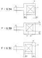
- Figs. 3A to 3C illustrate some examples of matching deviation between the connection hole 11 and the wiring layer 12.
- Fig. 3A shows a case where the connection hole 11 deviates in the direction opposite to the wiring extension side.
- resistances R3 and R3' inevitably increase.
- electrical current i3 which is affected by the resistances, occupies a very little portion of the whole current.
- resistances R2 and R2' decrease; therefore there is little change in connection hole resistance as a whole.
- Fig. 3B shows a case where the connection hole 11 deviates in the vertical direction to the wiring extension side.
- resistances (R2 + R3) and (R2' + R3') complimentarily increase and decrease canceling with each other, whereby the connection hole resistance is little affected as a whole.
- Fig. 3C shows a case where the connection hole 11 deviates towards the wiring extension side.
- the connection hole resistance inevitably increases. More specifically, current flows through all of resistances r1, R2 and R3. As around width B2 narrows, currents I2 and I2' flowing through resistances R2 and R2' decrease, and current i1 flowing through resistance r1, which becomes high inevitably due to structure, increases. Therefore, the matching deviation directly affects the connection hole resistance to increase, and disconnection of the wiring due to heat-emission or electromigration may occur at the notch S.
- the object of the present invention is to provide a wiring pattern of a semiconductor integrated circuit device in which the connection hole resistance does not increase even if matching deviation between a connection hole such as a contact hole or through hole, and a wiring layer occurs.
- the wiring pattern of the semiconductor integrated circuit device comprises a wiring portion extending from the connection hole and a connection portion located above the connection hole and connected to the wiring portion so that it makes an obtuse angle, in which a matching allowance for the connection hole on the wiring portion side is formed wider than the regular matching allowance by a predetermined width with which a required yield of successful matching can be assured.
- Fig. 4 shows a wiring pattern of a semiconductor integral circuit according to an embodiment of the present invention, including a semiconductor substrate 21, a connection hole 22, a wiring layer 23, a wiring width A, matching allowances between the connection hole and the wiring layer B and C, a wiring portion P, and a connection portion Q.
- connection hole 22 such as a contact hole or through hole is formed on the semiconductor substrate 21, and the wiring layer 23 is formed on the connection hole 22.
- the wiring layer 23 consists of the wiring portion P, which is a wiring portion extending in one direction from a side of the square-shaped connection hole 22, and connection portion Q, which is a wiring portion located on the connection hole 22.
- the matching allowance B on the wiring portion P side of the connection portion Q is formed so that it has a predetermined width, in other words, a width with which a sufficient current path can be obtained when the matching deviation of the wiring layer 23 is set to zero.
- the matching allowance B on the wiring portion P side is set so that it is a predetermined width wider than the regular matching allowance to cover the necessary matching efficiency.
- the matching allowance C at the sides other than the wiring portion P side is set to an appropriate width so that the pattern of the wiring layer 23 does not become too large.
- the minimum around width of the wiring portion P side for obtaining a sufficient electric current path is about 1.0 ⁇ m.
- the required yield of the successful allowance is 3 ⁇ ( ⁇ is a value for dispersion in the normal distribution)
- the predetermined width with which 3 ⁇ can be assured is about 0.5 ⁇ m
- the allowance B on the wiring portion P side should be set to about 1.5 ⁇ m to obtain a sufficient current path.
- the around width is about 1.5 ⁇ m as originally designed for the width of the matching allowance B. Even if the matching deviation of the wiring is as much as 0.5 ⁇ m in the direction opposite to the wiring portion P, the around width of about 1.0 ⁇ can be assured.
- the matching allowances C for the sides other than the wiring portion P side are set to about 0.7 ⁇ m so as to obtain an around width of, for example, about 0.2 ⁇ at a minimum. This is because, if the width of the matching allowances C are set to the same as that of the matching allowance B, the size of the wiring pattern of the wiring layer 23 around the connection hole 22 becomes very large lowering the degree of integration.
- the matching allowances other than that of the wiring portion P side should only be set to a minimally necessary width so that the wiring pattern does not become too large.
- the wiring width A is set to about 2 ⁇ m
- the size of the connection hole is set to about 3.0 ⁇ 3.0 ⁇ .
- the matching allowance B of the wiring portion P side is set a predetermined width wider than the predetermined allowance so as to cover matching deviation even in the case where the wiring layer deviates in the direction opposite to the wiring portion P side. Specifically, even if the wiring layer 23 deviates in the direction opposite to the wiring portion P side, a sufficient around width can be obtained within the range of the successful yield of matching allowance, whereby the contact hole resistance is not increased.
- connection hole resistance where the wiring layer 23 includes the matching allowance B of about 1.5 ⁇ m and the matching allowances C of about 0.7 ⁇ m was measured and the result is shown in Fig. 5 as represented by straight line II.
- line I when the amount of deviation in the direction opposite to the wiring portion P side is within 1.0 ⁇ m, in other words, the around width is in the range of 0.5-1.5 ⁇ m in the wiring layer 23, no increment in the connection hole resistance was not detected.
- the connection hole resistance in the case where the matching allowances for all sides of the connection hole 22 are equally set to about 1.0 ⁇ was measured and the result is also shown in this figure as represented by curve I.
- the present invention was applied to a bipolar LSI (A/D converter) having 4,500 elements, and no decrement in the degree of integration was not detected.
- Fig. 6 shows a wiring pattern of a semiconductor integrated circuit device according to another embodiment of the present invention.
- connection hole 22 such as a contact hole or through hole is formed on the semiconductor substrate 21, and the wiring layer 23 is formed on the connection hole 22.
- the wiring portion P and the contact portion Q are connected so that it makes an obtuse angle ( ⁇ /2 ⁇ ⁇ ) therebetween.
- the first embodiment mentioned above is a case where the wiring portion P and the contact portion Q are connected at right angle.
- the matching allowance B of the wiring portion P side is formed wider than a predetermined width so as to assure a sufficient current path when the matching deviation of matching pattern is set to zero.
- the matching allowance B is formed wider than the predetermined matching allowance by a predetermined width which assures the required yield of successful allowance.
- the minimum around width of the wiring portion P side for obtaining a sufficient electric current path is about 1.0 ⁇ m.
- the required yield of the successful allowance is 3 ⁇ ( ⁇ is a value for dispersion in the normal distribution)
- the predetermined width with which 3 ⁇ can be assured is about 0.5 ⁇ m
- the allowance B on the wiring portion P side should be set to about 1.5 ⁇ m to obtain a sufficient current path.
- the matching allowances other than the wiring portion P side are designed to be about 0.7 ⁇ m so as to obtain an around width of, for example, about 0.2 ⁇ at a minimum.
- the matching allowance B is, in advance, formed wider than the predetermined matching allowance by a predetermined width with which the actual matching deviation can be covered. Therefore, even if the wiring layer 23 deviates in the direction opposite to the wiring portion P side, the necessary around width can be obtained, and therefore the connection hole resistance does not increase.
- the above-described embodiments include the cases where there is only one wiring portion P; however, the present invention, of course, can be applied for the case where there are more than one wiring portion P, for example, as shown in Fig. 7. In this case also, there will not be any problem if the matching allowances B of each of the wiring portions P is formed wider than a predetermined matching allowance by a width with which a required yield can be assured.
Landscapes
- Internal Circuitry In Semiconductor Integrated Circuit Devices (AREA)
- Design And Manufacture Of Integrated Circuits (AREA)
- Semiconductor Integrated Circuits (AREA)
Applications Claiming Priority (3)
| Application Number | Priority Date | Filing Date | Title |
|---|---|---|---|
| JP1293490A JPH03154341A (ja) | 1989-11-10 | 1989-11-10 | 半導体装置 |
| JP293490/89 | 1989-11-10 | ||
| EP90121295A EP0427226B1 (de) | 1989-11-10 | 1990-11-07 | Verfahren zur Herstellung eines Leitermusters einer integrierten Schaltungshalbleiteranordnung |
Related Parent Applications (3)
| Application Number | Title | Priority Date | Filing Date |
|---|---|---|---|
| EP90121295A Division EP0427226B1 (de) | 1989-11-10 | 1990-11-07 | Verfahren zur Herstellung eines Leitermusters einer integrierten Schaltungshalbleiteranordnung |
| EP90121295A Division-Into EP0427226B1 (de) | 1989-11-10 | 1990-11-07 | Verfahren zur Herstellung eines Leitermusters einer integrierten Schaltungshalbleiteranordnung |
| EP90121295.1 Division | 1990-11-07 |
Publications (3)
| Publication Number | Publication Date |
|---|---|
| EP0702407A2 true EP0702407A2 (de) | 1996-03-20 |
| EP0702407A3 EP0702407A3 (de) | 1997-01-29 |
| EP0702407B1 EP0702407B1 (de) | 2006-01-11 |
Family
ID=17795414
Family Applications (2)
| Application Number | Title | Priority Date | Filing Date |
|---|---|---|---|
| EP90121295A Expired - Lifetime EP0427226B1 (de) | 1989-11-10 | 1990-11-07 | Verfahren zur Herstellung eines Leitermusters einer integrierten Schaltungshalbleiteranordnung |
| EP95117510A Expired - Lifetime EP0702407B1 (de) | 1989-11-10 | 1990-11-07 | Leitermuster einer integrierten Halbleiterschaltungsanordnung |
Family Applications Before (1)
| Application Number | Title | Priority Date | Filing Date |
|---|---|---|---|
| EP90121295A Expired - Lifetime EP0427226B1 (de) | 1989-11-10 | 1990-11-07 | Verfahren zur Herstellung eines Leitermusters einer integrierten Schaltungshalbleiteranordnung |
Country Status (5)
| Country | Link |
|---|---|
| US (4) | US5126819A (de) |
| EP (2) | EP0427226B1 (de) |
| JP (1) | JPH03154341A (de) |
| KR (1) | KR930010077B1 (de) |
| DE (2) | DE69033802T2 (de) |
Cited By (1)
| Publication number | Priority date | Publication date | Assignee | Title |
|---|---|---|---|---|
| DE3801331A1 (de) * | 1988-01-19 | 1989-07-27 | Gefinex Gmbh | Zielscheibe zum bogenschiessen |
Families Citing this family (11)
| Publication number | Priority date | Publication date | Assignee | Title |
|---|---|---|---|---|
| JPH03154341A (ja) * | 1989-11-10 | 1991-07-02 | Toshiba Corp | 半導体装置 |
| EP0480580A3 (en) * | 1990-09-10 | 1992-09-02 | Canon Kabushiki Kaisha | Electrode structure of semiconductor device and method for manufacturing the same |
| US5539156A (en) * | 1994-11-16 | 1996-07-23 | International Business Machines Corporation | Non-annular lands |
| US5506450A (en) * | 1995-05-04 | 1996-04-09 | Motorola, Inc. | Semiconductor device with improved electromigration resistance and method for making the same |
| KR100215847B1 (ko) * | 1996-05-16 | 1999-08-16 | 구본준 | 반도체 장치의 금속 배선 및 그의 형성 방법 |
| US6081035A (en) * | 1996-10-24 | 2000-06-27 | Tessera, Inc. | Microelectronic bond ribbon design |
| DE19743264C2 (de) * | 1997-09-30 | 2002-01-17 | Infineon Technologies Ag | Verfahren zur Herstellung einer Emulationsschaltkreisanordnung sowie Emulationsschaltkreisanordnung mit zwei integrierten Schaltkreisen |
| US6103623A (en) * | 1998-10-05 | 2000-08-15 | Vanguard International Semiconductor Corporation | Method for fabricating a tungsten plug structure and an overlying interconnect metal structure without a tungsten etch back or CMP procedure |
| US7183653B2 (en) * | 2003-12-17 | 2007-02-27 | Intel Corporation | Via including multiple electrical paths |
| US8089160B2 (en) * | 2007-12-12 | 2012-01-03 | International Business Machines Corporation | IC interconnect for high current |
| JP5552261B2 (ja) * | 2009-05-12 | 2014-07-16 | パナソニック株式会社 | 半導体装置 |
Family Cites Families (21)
| Publication number | Priority date | Publication date | Assignee | Title |
|---|---|---|---|---|
| US4196443A (en) * | 1978-08-25 | 1980-04-01 | Rca Corporation | Buried contact configuration for CMOS/SOS integrated circuits |
| US4381215A (en) * | 1980-05-27 | 1983-04-26 | Burroughs Corporation | Method of fabricating a misaligned, composite electrical contact on a semiconductor substrate |
| JPS57112027A (en) * | 1980-12-29 | 1982-07-12 | Fujitsu Ltd | Manufacture of semiconductor device |
| JPS57201171A (en) * | 1981-06-02 | 1982-12-09 | Meinan Mach Works Inc | Polishing device |
| JPS5914649A (ja) * | 1982-07-16 | 1984-01-25 | Nec Corp | 半導体装置 |
| JPS59169150A (ja) * | 1983-03-16 | 1984-09-25 | Hitachi Ltd | 多層配線構造 |
| JPS59188149A (ja) * | 1984-04-02 | 1984-10-25 | Hitachi Ltd | 半導体装置 |
| JPS60208845A (ja) * | 1984-04-02 | 1985-10-21 | Oki Electric Ind Co Ltd | 半導体装置の配線形成法 |
| US4577212A (en) * | 1984-06-29 | 1986-03-18 | International Business Machines Corporation | Structure for inhibiting forward bias beta degradation |
| JPS61131469A (ja) * | 1984-11-29 | 1986-06-19 | Fujitsu Ltd | 半導体装置の製造方法 |
| JPS61194848A (ja) * | 1985-02-25 | 1986-08-29 | Hitachi Ltd | 半導体装置 |
| JPS60242643A (ja) * | 1985-03-22 | 1985-12-02 | Hitachi Ltd | 電子部品の配線 |
| JPS6378554A (ja) * | 1986-09-20 | 1988-04-08 | Mitsubishi Electric Corp | 半導体装置 |
| US4812419A (en) * | 1987-04-30 | 1989-03-14 | Hewlett-Packard Company | Via connection with thin resistivity layer |
| JPS63292672A (ja) * | 1987-05-26 | 1988-11-29 | Nec Corp | 半導体装置 |
| JPH01191914A (ja) * | 1988-01-27 | 1989-08-02 | Toshiba Corp | コンピュータシステム |
| JPH01191195A (ja) * | 1988-01-27 | 1989-08-01 | Toshiba Corp | 表示システム |
| JPH01305531A (ja) * | 1988-06-03 | 1989-12-08 | Nec Corp | 改良されたボンディングパッドを有する半導体装置 |
| JPH0277090A (ja) * | 1988-09-13 | 1990-03-16 | Toshiba Corp | 表示構成設定方式 |
| JPH0379059A (ja) * | 1989-08-22 | 1991-04-04 | Hitachi Ltd | 半導体集積回路装置およびその製造方法 |
| JPH03154341A (ja) * | 1989-11-10 | 1991-07-02 | Toshiba Corp | 半導体装置 |
-
1989
- 1989-11-10 JP JP1293490A patent/JPH03154341A/ja active Granted
-
1990
- 1990-11-06 US US07/609,601 patent/US5126819A/en not_active Expired - Lifetime
- 1990-11-07 DE DE69033802T patent/DE69033802T2/de not_active Expired - Lifetime
- 1990-11-07 KR KR1019900017927A patent/KR930010077B1/ko not_active Expired - Lifetime
- 1990-11-07 EP EP90121295A patent/EP0427226B1/de not_active Expired - Lifetime
- 1990-11-07 DE DE69034215T patent/DE69034215T2/de not_active Expired - Lifetime
- 1990-11-07 EP EP95117510A patent/EP0702407B1/de not_active Expired - Lifetime
-
1993
- 1993-06-18 US US08/077,946 patent/US5411916A/en not_active Expired - Lifetime
-
1995
- 1995-01-20 US US08/375,690 patent/US5523627A/en not_active Ceased
-
1998
- 1998-06-04 US US09/090,401 patent/USRE37059E1/en not_active Expired - Lifetime
Non-Patent Citations (1)
| Title |
|---|
| None |
Cited By (1)
| Publication number | Priority date | Publication date | Assignee | Title |
|---|---|---|---|---|
| DE3801331A1 (de) * | 1988-01-19 | 1989-07-27 | Gefinex Gmbh | Zielscheibe zum bogenschiessen |
Also Published As
| Publication number | Publication date |
|---|---|
| EP0702407B1 (de) | 2006-01-11 |
| USRE37059E1 (en) | 2001-02-20 |
| US5523627A (en) | 1996-06-04 |
| US5411916A (en) | 1995-05-02 |
| DE69033802D1 (de) | 2001-10-25 |
| EP0427226A3 (en) | 1991-08-21 |
| EP0427226A2 (de) | 1991-05-15 |
| EP0702407A3 (de) | 1997-01-29 |
| US5126819A (en) | 1992-06-30 |
| EP0427226B1 (de) | 2001-09-19 |
| JPH0578172B2 (de) | 1993-10-28 |
| DE69034215D1 (de) | 2006-04-06 |
| DE69034215T2 (de) | 2006-09-21 |
| KR930010077B1 (ko) | 1993-10-14 |
| KR910010688A (ko) | 1991-06-29 |
| DE69033802T2 (de) | 2002-04-04 |
| JPH03154341A (ja) | 1991-07-02 |
Similar Documents
| Publication | Publication Date | Title |
|---|---|---|
| KR0162247B1 (ko) | 가요성 인쇄회로 | |
| EP0702407A2 (de) | Leitermuster einer integrierten Halbleiterschaltungsanordnung | |
| DE102009054892B4 (de) | Magnetfeldstromsensoren und Verfahren | |
| EP0516402B1 (de) | Mit elektrischen Leitungen versehenes Substrat und dessen Herstellungsverfahren | |
| US7089652B2 (en) | Method of manufacturing flip chip resistor | |
| US20060060962A1 (en) | Electronic package having a folded package substrate | |
| US4209798A (en) | Module for integrated circuits | |
| JPS60500111A (ja) | 半導体チツプパツケ−ジ | |
| US6316827B1 (en) | Semiconductor device having improved temperature distribution | |
| JP4029049B2 (ja) | 電流検出用抵抗器 | |
| US5309020A (en) | Packaged semiconductor device assembly including two interconnected packaged semiconductor devices mounted on a common substrate | |
| KR100380514B1 (ko) | 집적회로및그동작방법 | |
| KR100397079B1 (ko) | 전계효과에의해제어가능한반도체소자 | |
| US5640097A (en) | Test pattern for separately determining plug resistance and interfactial resistance | |
| JP4050151B2 (ja) | 電気的接続素子を備えた集積回路 | |
| JPH057868B2 (de) | ||
| CN115362355A (zh) | 用于温度测量的设备和用于电流求取的设备 | |
| KR100634238B1 (ko) | 테이프 캐리어 패키지용 탭 테이프 | |
| US6346721B1 (en) | Integrated circuit having radially varying power bus grid architecture | |
| JPH10200221A (ja) | 大電流用プリント基板 | |
| KR20010039790A (ko) | 집적 반도체 칩 | |
| US5374848A (en) | Thermal stress resistant semiconductor device mounting arrangement | |
| RU2216080C2 (ru) | Защитный соединитель для телекоммуникационного устройства | |
| JP2797971B2 (ja) | 複合プリント基板の接続構造 | |
| KR920003316B1 (ko) | 전자장치의 도선들을 접속하기 위한 접속구조 |
Legal Events
| Date | Code | Title | Description |
|---|---|---|---|
| PUAI | Public reference made under article 153(3) epc to a published international application that has entered the european phase |
Free format text: ORIGINAL CODE: 0009012 |
|
| 17P | Request for examination filed |
Effective date: 19951107 |
|
| AC | Divisional application: reference to earlier application |
Ref document number: 427226 Country of ref document: EP |
|
| AK | Designated contracting states |
Kind code of ref document: A2 Designated state(s): DE FR GB |
|
| PUAL | Search report despatched |
Free format text: ORIGINAL CODE: 0009013 |
|
| AK | Designated contracting states |
Kind code of ref document: A3 Designated state(s): DE FR GB |
|
| 17Q | First examination report despatched |
Effective date: 19981124 |
|
| GRAP | Despatch of communication of intention to grant a patent |
Free format text: ORIGINAL CODE: EPIDOSNIGR1 |
|
| GRAS | Grant fee paid |
Free format text: ORIGINAL CODE: EPIDOSNIGR3 |
|
| GRAA | (expected) grant |
Free format text: ORIGINAL CODE: 0009210 |
|
| AC | Divisional application: reference to earlier application |
Ref document number: 0427226 Country of ref document: EP Kind code of ref document: P |
|
| AK | Designated contracting states |
Kind code of ref document: B1 Designated state(s): DE FR GB |
|
| REF | Corresponds to: |
Ref document number: 69034215 Country of ref document: DE Date of ref document: 20060406 Kind code of ref document: P |
|
| ET | Fr: translation filed | ||
| PLBE | No opposition filed within time limit |
Free format text: ORIGINAL CODE: 0009261 |
|
| STAA | Information on the status of an ep patent application or granted ep patent |
Free format text: STATUS: NO OPPOSITION FILED WITHIN TIME LIMIT |
|
| 26N | No opposition filed |
Effective date: 20061012 |
|
| PGFP | Annual fee paid to national office [announced via postgrant information from national office to epo] |
Ref country code: DE Payment date: 20091105 Year of fee payment: 20 |
|
| PGFP | Annual fee paid to national office [announced via postgrant information from national office to epo] |
Ref country code: GB Payment date: 20091104 Year of fee payment: 20 Ref country code: FR Payment date: 20091123 Year of fee payment: 20 |
|
| REG | Reference to a national code |
Ref country code: GB Ref legal event code: PE20 Expiry date: 20101106 |
|
| PG25 | Lapsed in a contracting state [announced via postgrant information from national office to epo] |
Ref country code: GB Free format text: LAPSE BECAUSE OF EXPIRATION OF PROTECTION Effective date: 20101106 |
|
| PG25 | Lapsed in a contracting state [announced via postgrant information from national office to epo] |
Ref country code: DE Free format text: LAPSE BECAUSE OF EXPIRATION OF PROTECTION Effective date: 20101107 |