EP0703584A1 - Integriertes Speicheradressen-Dekodierverfahren und Speicherschaltung unter Verwendung eines solchen Verfahrens - Google Patents
Integriertes Speicheradressen-Dekodierverfahren und Speicherschaltung unter Verwendung eines solchen Verfahrens Download PDFInfo
- Publication number
- EP0703584A1 EP0703584A1 EP95402054A EP95402054A EP0703584A1 EP 0703584 A1 EP0703584 A1 EP 0703584A1 EP 95402054 A EP95402054 A EP 95402054A EP 95402054 A EP95402054 A EP 95402054A EP 0703584 A1 EP0703584 A1 EP 0703584A1
- Authority
- EP
- European Patent Office
- Prior art keywords
- row
- circuit
- address
- signal
- voltage
- Prior art date
- Legal status (The legal status is an assumption and is not a legal conclusion. Google has not performed a legal analysis and makes no representation as to the accuracy of the status listed.)
- Granted
Links
- 230000015654 memory Effects 0.000 title claims abstract description 44
- 238000000034 method Methods 0.000 title claims abstract description 11
- 238000001914 filtration Methods 0.000 claims abstract description 36
- 230000008859 change Effects 0.000 claims abstract description 17
- 238000001514 detection method Methods 0.000 claims description 26
- 230000007704 transition Effects 0.000 claims description 17
- 230000005764 inhibitory process Effects 0.000 claims description 14
- 230000002401 inhibitory effect Effects 0.000 claims description 3
- 150000003839 salts Chemical class 0.000 claims description 3
- 230000004044 response Effects 0.000 claims description 2
- 239000003990 capacitor Substances 0.000 description 4
- 238000010586 diagram Methods 0.000 description 4
- 238000002955 isolation Methods 0.000 description 4
- 238000010200 validation analysis Methods 0.000 description 4
- 230000000903 blocking effect Effects 0.000 description 2
- 208000037516 chromosome inversion disease Diseases 0.000 description 2
- 238000005516 engineering process Methods 0.000 description 2
- 239000011159 matrix material Substances 0.000 description 2
- 241001296405 Tiso Species 0.000 description 1
- 230000004913 activation Effects 0.000 description 1
- 238000013475 authorization Methods 0.000 description 1
- 230000007423 decrease Effects 0.000 description 1
- 230000003111 delayed effect Effects 0.000 description 1
- 230000000694 effects Effects 0.000 description 1
- 238000009413 insulation Methods 0.000 description 1
- 230000010354 integration Effects 0.000 description 1
- 230000003071 parasitic effect Effects 0.000 description 1
- 230000008569 process Effects 0.000 description 1
- 238000012163 sequencing technique Methods 0.000 description 1
Images


Classifications
-
- G—PHYSICS
- G11—INFORMATION STORAGE
- G11C—STATIC STORES
- G11C8/00—Arrangements for selecting an address in a digital store
- G11C8/08—Word line control circuits, e.g. drivers, boosters, pull-up circuits, pull-down circuits, precharging circuits, for word lines
-
- G—PHYSICS
- G11—INFORMATION STORAGE
- G11C—STATIC STORES
- G11C8/00—Arrangements for selecting an address in a digital store
- G11C8/10—Decoders
-
- G—PHYSICS
- G11—INFORMATION STORAGE
- G11C—STATIC STORES
- G11C8/00—Arrangements for selecting an address in a digital store
- G11C8/18—Address timing or clocking circuits; Address control signal generation or management, e.g. for row address strobe [RAS] or column address strobe [CAS] signals
Definitions
- the invention relates to a method for decoding an address in an integrated circuit memory, and a corresponding memory.
- a voltage multiplier is notably characterized by its number of transistors and capacitors, its internal resistance and its ability to deliver a given current for a given time and at an output voltage as constant as possible: in other words, for a given output load, the given time after which the output voltage will start to collapse. This last characteristic is particularly sensitive, hampering the use of multipliers in circuits with high current consumption, unless using an expensive structure on the surface and very current consuming (number and characteristics of the transistors and capacitors).
- Asynchronous memory circuits that is to say not receiving an external clock signal, can receive data all the time: this data is immediately taken into account and the corresponding operations carried out.
- the addresses which appear are immediately decoded: the access time of these memories is thus very efficient.
- low-voltage asynchronous memories they are therefore able to take into account a new address very quickly: the corresponding rows and columns of the memory are selected and the control voltages applied.
- reading which is generally the default access mode, the reading voltage supplied by the multiplier is applied to the addressed row.
- the memory addresses are supplied by an external bus which may be noisy (parasitic) or shared with other integrated circuits. If the memory decoder takes into account all the address changes on the external bus, we select at very close rates different rows (which are capacitive lines) to which the voltage from the multiplier is successively applied: the multiplier n has more time to recharge between two row selections and collapses: the voltage at the output of the multiplier dangerously decreases towards zero before gradually increasing, the recharging time of the multiplier being particularly long, of the order of hundred nanoseconds.
- the invention proposes to solve this problem of collapse of the reading voltage of the rows incompatible with the access time of the memory.
- the invention relates to a method for decoding the addresses of a memory.
- an address decoding inhibition command is generated for a duration d1.
- the invention also relates to an integrated circuit memory comprising an address decoder for selecting memory cells.
- the memory includes a circuit for filtering address changes to inhibit said address decoder for a determined period d1 after detection of a change of address.
- the invention applies to the filtering of addresses of rows of the memory.
- the decoder comprising a row decoder and a column decoder
- the filtering circuit transmits a filtering signal applied to the row decoder.
- the row decoder comprising an address decoding circuit for selecting a row and deselecting the others, and a voltage switching circuit in the rows, it further comprises an inhibition circuit which receives the input signal filtering, to inhibit the voltage switching circuit.
- the decoding of the address is carried out permanently, only the switching of the read voltage on the row is inhibited. In this way, the access time to the memory is practically unchanged, the decoding of the address being slower than the voltage switching on the rows.
- the inhibition duration is chosen on the order of the maximum duration necessary for decoding the address (worst case).
- an address detection circuit and a pulse generation circuit of determined duration on receipt of an input pulse are used.
- Address transition or transition detection circuits on circuit control or validation signals are conventionally used in asynchronous circuits, to generate the internal clocks necessary for the sequencing of the operations to be executed. Conversely, when there is no address transition, they are used to generate a circuit standby signal, allowing very low consumption of the circuit.
- the operating principle of an address detection circuit is to compare the current state of an input signal to the previously memorized state, to memorize the current state if it is different from the previous memorized state. and generate an output pulse.
- Pulse generation circuits are also used in these same asynchronous circuits, at the output of the address transition detection circuit, to generate the internal clocks.
- the matrix memory plane 1 consists of columns connected to the cell drains and rows connected to the cell grids.
- the cells are produced in the example in floating gate MOS technology. However, the invention is not limited to this example.
- a decoder 2 thus comprises a decoder of rows DR and a decoder of columns DC.
- An address presented by an external address bus BA is stored in an address register 3 connected as an output to the address bus of the memory, denoted ADR.
- the internal address bus ADR is divided into two parts: row address applied as input to the row decoder DR and column address applied as input to the column decoder DC, coded in the example respectively on the address bits a0-a7 and a8-a15.
- the row decoder directly controls the rows of the memory: it applies a control voltage Vr to the addressed row, and puts the other rows to ground (Vss).
- the control voltage can be a read or write voltage.
- the column decoder controls a gate circuit 4 which applies the control voltage (Vc) to the addressed column (s) and the ground (Vss) to the others and connects the columns to the data input or output circuits, grouped under the reference 5 and connected to the external data input / output bus BD of the memory.
- Vc control voltage
- Vss ground
- the column and row control voltages are for example from a voltage generation circuit 6, receiving the voltages Vcc and Vss as input. It notably includes a multiplier circuit 6m receiving as input the low operating voltage Vcc, for example of the order of 3 volts and which provides a reading voltage of the order of 5 volts for the voltage Vr for controlling the rows.
- the memory architecture further comprises a circuit 7 for filtering addresses.
- This circuit is connected at input to the internal address bus ADR and outputs a filtering signal f applied at input to decoder 2 of the memory.
- this filtering circuit makes it possible to filter the excessively rapid address transitions, by inhibiting the decoder 2 for a period d1 after the detection of any change of address on the internal address bus ADR.
- this circuit 7 thus includes a circuit 8 for detecting a transition on each of the address bits, a logic OR gate circuit 9 for delivering change of information information d address as soon as at least one transition on an address bit is detected and a circuit 10 generating a pulse of duration d1 on the filtering signal f.
- the address transition detection circuit 8 comprises a detection stage per address bit to be taken into account: each stage 8i receives as input address bit noted ai and delivers a corresponding detection signal at output noted ati.
- a stage 8i comprises for example a flip-flop Di and an exclusive OR gate Xi.
- the input D of the flip-flop receives the address bit ai and the output Q of the flip-flop delivers a signal Qi.
- the exclusive OR gate Xi receives on an input the address bit ai and on another input, the signal Qi.
- the output of the exclusive OR gate delivers the detection signal ati and this signal is looped back to the clock input (H) of the scale.
- the operating principle is simple. To detect an address transition, it is necessary to store the previous high or low logic state, which allows the flip-flop Di which stores the previous state on its output Q.
- the state of the corresponding signal Qi is compared by permanence in the OR gate exclusive to the current state of the address bit ai.
- the output ati of the gate Xi is at a first logic level (0, in the example) as long as the signals ai and Qi have the same logic level. As soon as the signals ai and Qi have different logic states, the output of the gate Xi goes to a second logic level (1 in the example).
- the passage from the first level (0) to the second level (1) which corresponds to the detection of a transition on the address bit ai causes the memorization of the current state of the bit ai which is applied to the input D of the rocker.
- the signals ai and Qi then again have the same logic state and the output of the gate Xi returns to the first logic level (0).
- the detection of an address transition on the bit ai therefore generates a very short pulse on the ati output.
- the ati address transition detection signals are applied at the input of the OR gate circuit 9, to output an Sd signal of address change detection corresponding to a transition on at least one address bit.
- This signal Sd is applied to the pulse generation circuit 10, which generates a determined duration pulse d1 in response to the change of address detection pulse.
- a pulse generation circuit may include a charge and discharge control inverter of a capacitor and a circuit for reshaping the signal supplied by the capacitor. Other more complex embodiments are possible. These commonly used circuits are well known to those skilled in the art.
- the determined duration pulse d1 emitted on the filtering signal f inhibits the decoder 2 during this duration. In practice, therefore, only the addresses present on the address bus ADR are decoded for at least this period d1.
- FIG. 3 illustrates the operation of the filtering circuit.
- a change of address detection pulse is sent at the output Sd of the OR gate.
- the corresponding filtering signal f therefore comprises a first long pulse, which begins on the first address detection pulse and stops after the last duration d1 controlled by the seventh change of address detection pulse. Then another pulse is issued of duration d1, on the detection of the next change of address, the address remaining stable thereafter.
- the filtering signal will therefore be more particularly applied according to the invention to the row decoder DR.
- the filtering circuit preferably receives only the row address bits, a0-a7 in the example (FIG. 2).
- the decoder performs on the one hand the row address decoding to select the corresponding row and on the other hand controls the application of the necessary voltages on the rows: control voltage Vr on the selected row and zero voltage (Vss) on the other rows, which we will say are they, deselected.
- the decoder therefore comprises a pure decoding circuit and a voltage switching circuit.
- the filtering signal is then advantageously used (in an inhibition circuit) to inhibit the voltage switching circuit of the row decoder: thus the address decoding is carried out continuously, in parallel with the detection change of address and only the switching of voltages is inhibited by the filtering signal. If in the meantime the selection of the row disappears, the voltages will not be applied.
- the switching command of the voltage Vr is filtered on the selected row.
- Vss the zero voltage which is applied to it, which does not pose a problem of collapse of the voltage generated by the multiplier 6m.
- the switching of the zero voltage (Vss) if the line was previously selected (at Vr), is slower than the switching of the voltage Vr.
- the row decoder thus advantageously comprises for each row an inhibition circuit receiving as input the filtering signal f and a row selection control signal, and delivering as output a filtered selection control signal row applied to a voltage switching circuit (Vr) on the selected row.
- Vr voltage switching circuit
- the block address is coded on 4 bits, a5-a7, the row address is coded on 5 bits, a0-a4.
- the row decoder comprises k block address decoders delivering block validation signals. For each block address decoder, there are 32 row address decoders. Each row address decoder provides a selection control signal and a deselection control signal of the corresponding row.
- the row decoder also includes, associated with each block, 32 voltage switching circuits in a row. Each circuit is validated by the signals of the address decoder of the associated block and receives as input the selection control signal and the deselection control signal of the address decoder of the row to which it is connected as output and on which it switches the voltage Vr supplied by the voltage generation circuit 6 (selection) or the voltage Vss (deselection).
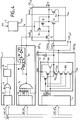
- the NAND gate with two isolated outputs is explained in CMOS technology in FIG. 4.
- the isolation is obtained in known manner by inserting an isolation transistor Tiso between a serial network RN of transistors N and a parallel network RP of transistors P.
- An output comn2 is taken between the output of the parallel network and the isolation transistor, the other output comp2 is taken between the isolation transistor and the input of the serial network (the output comp2 is the one that controls the switching of the voltage Vr, as will be seen below, hence the need for insulation between the two outputs).
- the decoder DECr4 of address row 4 of block B2 comprises a first circuit with inversion stage 14 and NAND gate 15 for decoding the address (4) of this group.
- the NAND gate also receives as input the signal VB2 for decoding validation delivered by the decoder of the associated block DECB2.
- the NAND gate is followed by an inverter 16 which outputs a sel signal 4.2 of row selection command.
- a deselection control signal dsel 4'2 of the address row 4 of the block B2 is delivered directly by the output of the NAND gate.
- the row decoder further comprises an inhibition circuit 17 receiving as input the filtering signal f supplied by the filtering 7 according to the invention and the sel row selector control signal 4.2 , to provide a selection control signal which is filtered according to the method of the invention, denoted fsel 4.2 .
- This inhibition circuit comprises in the example a first NAND gate 18 followed in series by an inverter 19.
- the selection control signal will be at logic "1", that is to say at approximately 3 volts in logic low-voltage and the deselection control signal dsel 4'2 will be at logic "0". Otherwise, it is the signal dsel 4'2 which will be at "1” and the signal salt 4.2 which will be at "0".
- the detection of a change of address on the bus generates a filtering signal f.
- the filtered selection command signal fsel 4.2 at the output of the inhibition circuit 17 according to the invention is therefore forced to logic "0" level for at least a period d1 upon detection of a change of address, in accordance with the timing diagram of FIG. 2. In fact, it is kept at zero as long as there is not a stable address for a duration greater than d1. Then, it takes the logic level of the sel sel sel command signal 4.2 : If row 4 of block B2 is effectively addressed, it therefore goes to logic level "1".
- control signals comp 2 ' comn 2' are active in the low state, noted “0” and corresponding at the zero logic voltage Vss and the signals fsel 4.2 and dsel 4'2 are active in the high state, noted “1” and corresponding to the high logic voltage, Vcc (3 volts in the example).
- the signal comn2 (“0") applied to the gate of the transistor Tn blocks it, while the selection transistor Ts is made passing by the signal fsel 4.2 ("1"): the transistor Tp of the inverter is therefore conducting and thus switches the voltage Vr on the row W 4.2 .
- row 4 of block B2 is deselected, it is the signal dsel 4'2 which becomes active ("1") and makes the deselection transistor Tds conductive, the transistors Ts and Tp being blocked. The row is then brought to Vss.
- the command signals comn2, comp2 are both at "1"
- the filtered selection command signal fsel 4.2 is at "0”
- the deselection command signal dsel 4 ' 2 is at "1”. Consequently, the transistors Ts and Tp are blocked, while the transistors Tn and Tds are on, which has the effect of maintaining (if the row was already deselected) or carrying (if the row was previously selected) the deselected row to ground.
- the blocking transistor Tb is on if the row is brought to ground: it thus puts the voltage Vr on the gate of the transistor Tp, which keeps it blocked.
- the filtered selection command signal fsel 4.2 is maintained at "0" by the inhibition circuit 17 as long as an address is not stable within the meaning of the invention (it is to say present for at least a period d1), the transistor Tp is blocked, preventing any current draw on the line of voltage Vr: The multiplier is therefore not requested until an address is not stable on the bus.
- the embodiment of the decoder which has just been explained in relation to FIG. 4 and more generally the inhibition of the selection command (salt 4.2 ) makes it possible to delay only the switching of the voltage Vr to the selected row. In particular, decoding and deselection are not delayed.
- the determined duration d1 corresponds to the maximum duration necessary for the decoding of the address, so that the filtering according to the invention has the least possible influence on the access time of the memory.
- the filtering method according to the invention makes it possible to make the operation of low-voltage asynchronous memories compatible with the use of an internal voltage multiplier, and its preferred embodiment advantageously makes it possible not to penalize the access time too much. Memory.
Landscapes
- Engineering & Computer Science (AREA)
- Microelectronics & Electronic Packaging (AREA)
- Dram (AREA)
- Static Random-Access Memory (AREA)
- Read Only Memory (AREA)
Applications Claiming Priority (2)
| Application Number | Priority Date | Filing Date | Title |
|---|---|---|---|
| FR9410833 | 1994-09-12 | ||
| FR9410833A FR2724483B1 (fr) | 1994-09-12 | 1994-09-12 | Procede de decodage d'adresse dans une memoire en circuit integre et circuit memoire mettant en oeuvre le procede |
Publications (2)
| Publication Number | Publication Date |
|---|---|
| EP0703584A1 true EP0703584A1 (de) | 1996-03-27 |
| EP0703584B1 EP0703584B1 (de) | 1998-04-22 |
Family
ID=9466839
Family Applications (1)
| Application Number | Title | Priority Date | Filing Date |
|---|---|---|---|
| EP95402054A Expired - Lifetime EP0703584B1 (de) | 1994-09-12 | 1995-09-11 | Adressen-Dekodierverfahren für einen integrierten Speicher und Speicherschaltung zur Anwendung eines solchen Verfahrens |
Country Status (5)
| Country | Link |
|---|---|
| US (1) | US5742546A (de) |
| EP (1) | EP0703584B1 (de) |
| JP (1) | JP3124713B2 (de) |
| DE (1) | DE69502155T2 (de) |
| FR (1) | FR2724483B1 (de) |
Cited By (1)
| Publication number | Priority date | Publication date | Assignee | Title |
|---|---|---|---|---|
| US6314099B1 (en) | 1997-11-28 | 2001-11-06 | Mitsubishi Electric System Lsi Design Corporation | Address match determining device, communication control system, and address match determining method |
Families Citing this family (8)
| Publication number | Priority date | Publication date | Assignee | Title |
|---|---|---|---|---|
| US5762193A (en) | 1996-10-23 | 1998-06-09 | Illinois Tool Works Inc. | Clip-on sheet for container carrier |
| FR2762708B1 (fr) * | 1997-04-29 | 1999-06-04 | Sgs Thomson Microelectronics | Procede de commande d'une cellule memoire et memoire non volatile programmable une seule fois en technologie cmos |
| US20050035429A1 (en) * | 2003-08-15 | 2005-02-17 | Yeh Chih Chieh | Programmable eraseless memory |
| US7768865B2 (en) * | 2008-04-21 | 2010-08-03 | Vikram Bollu | Address decoder and/or access line driver and method for memory devices |
| US8363766B2 (en) * | 2008-06-06 | 2013-01-29 | Freescale Semiconductor, Inc. | Device and method of synchronizing signals |
| GB2472015B (en) * | 2009-07-21 | 2011-06-15 | Andrew Gordon Cameron Bruce | Cranks powered by each individual leg, ankle and foot bicycle pedal cranks |
| US8477555B2 (en) * | 2011-06-30 | 2013-07-02 | Intel Corporation | Deselect drivers for a memory array |
| CN119512992B (zh) * | 2024-10-28 | 2026-01-23 | 湖南开鸿智谷数字产业发展有限公司 | 一种电路板通讯地址分配系统、方法、装置及存储介质 |
Citations (7)
| Publication number | Priority date | Publication date | Assignee | Title |
|---|---|---|---|---|
| JPS53117342A (en) * | 1977-03-23 | 1978-10-13 | Nec Corp | Memory unit |
| EP0030118A2 (de) * | 1979-11-29 | 1981-06-10 | Fujitsu Limited | Dekodierschaltung |
| EP0105757A2 (de) * | 1982-10-04 | 1984-04-18 | Fujitsu Limited | Asynchrone Halbleiterspeicheranordnung |
| EP0306392A1 (de) * | 1987-09-01 | 1989-03-08 | STMicroelectronics S.A. | Abfühlschaltung für Adressenumschaltungen |
| US4839787A (en) | 1987-05-20 | 1989-06-13 | Matsushita Electric Industrial Co., Ltd. | Integrated high voltage generating system |
| US5029135A (en) * | 1989-02-15 | 1991-07-02 | Ricoh Company, Ltd. | Semiconductor memory apparatus with internal synchronization |
| EP0558079A2 (de) * | 1992-02-28 | 1993-09-01 | Sony Corporation | Halbleiterspeicheranordnung mit einer Adressübergangsabfühlschaltung |
Family Cites Families (4)
| Publication number | Priority date | Publication date | Assignee | Title |
|---|---|---|---|---|
| JP2728679B2 (ja) * | 1988-06-27 | 1998-03-18 | 株式会社東芝 | 不揮発性半導体メモリ装置 |
| JPH04195894A (ja) * | 1990-11-27 | 1992-07-15 | Nec Ic Microcomput Syst Ltd | 非同期式ram |
| JP2734315B2 (ja) * | 1992-09-24 | 1998-03-30 | 日本電気株式会社 | 半導体メモリ装置 |
| JPH06236686A (ja) * | 1993-01-22 | 1994-08-23 | Nec Corp | 半導体装置 |
-
1994
- 1994-09-12 FR FR9410833A patent/FR2724483B1/fr not_active Expired - Fee Related
-
1995
- 1995-09-11 DE DE69502155T patent/DE69502155T2/de not_active Expired - Fee Related
- 1995-09-11 US US08/526,500 patent/US5742546A/en not_active Expired - Lifetime
- 1995-09-11 EP EP95402054A patent/EP0703584B1/de not_active Expired - Lifetime
- 1995-09-12 JP JP07259289A patent/JP3124713B2/ja not_active Expired - Fee Related
Patent Citations (7)
| Publication number | Priority date | Publication date | Assignee | Title |
|---|---|---|---|---|
| JPS53117342A (en) * | 1977-03-23 | 1978-10-13 | Nec Corp | Memory unit |
| EP0030118A2 (de) * | 1979-11-29 | 1981-06-10 | Fujitsu Limited | Dekodierschaltung |
| EP0105757A2 (de) * | 1982-10-04 | 1984-04-18 | Fujitsu Limited | Asynchrone Halbleiterspeicheranordnung |
| US4839787A (en) | 1987-05-20 | 1989-06-13 | Matsushita Electric Industrial Co., Ltd. | Integrated high voltage generating system |
| EP0306392A1 (de) * | 1987-09-01 | 1989-03-08 | STMicroelectronics S.A. | Abfühlschaltung für Adressenumschaltungen |
| US5029135A (en) * | 1989-02-15 | 1991-07-02 | Ricoh Company, Ltd. | Semiconductor memory apparatus with internal synchronization |
| EP0558079A2 (de) * | 1992-02-28 | 1993-09-01 | Sony Corporation | Halbleiterspeicheranordnung mit einer Adressübergangsabfühlschaltung |
Non-Patent Citations (1)
| Title |
|---|
| PATENT ABSTRACTS OF JAPAN vol. 2, no. 149 (E - 78) 13 December 1978 (1978-12-13) * |
Cited By (2)
| Publication number | Priority date | Publication date | Assignee | Title |
|---|---|---|---|---|
| US6314099B1 (en) | 1997-11-28 | 2001-11-06 | Mitsubishi Electric System Lsi Design Corporation | Address match determining device, communication control system, and address match determining method |
| DE19848241B4 (de) * | 1997-11-28 | 2004-08-26 | Mitsubishi Electric Semiconductor Application Engineering Corp. | Einrichtung und Verfahren zur Adressengleichheitsermittlung und Übertragungssteuersystem |
Also Published As
| Publication number | Publication date |
|---|---|
| DE69502155T2 (de) | 1998-08-13 |
| EP0703584B1 (de) | 1998-04-22 |
| FR2724483B1 (fr) | 1996-12-27 |
| FR2724483A1 (fr) | 1996-03-15 |
| JP3124713B2 (ja) | 2001-01-15 |
| US5742546A (en) | 1998-04-21 |
| JPH0887890A (ja) | 1996-04-02 |
| DE69502155D1 (de) | 1998-05-28 |
Similar Documents
| Publication | Publication Date | Title |
|---|---|---|
| EP0318363B1 (de) | Verfahren zum Testen von Zellen von elektrisch programmierbaren Speichern und entsprechende integrierte Schaltung | |
| FR2778012A1 (fr) | Dispositif et procede de lecture de cellules de memoire eeprom | |
| FR2689294A1 (fr) | Circuit de pompage de tension à utiliser dans des dispositifs de mémoire à semi-conducteur. | |
| EP0703584B1 (de) | Adressen-Dekodierverfahren für einen integrierten Speicher und Speicherschaltung zur Anwendung eines solchen Verfahrens | |
| FR2858874A1 (fr) | Dispositif de commande de memoire, carte a puce et procede de commande d'une operation de lecture d'une memoire | |
| FR2665973A1 (fr) | Circuit d'optimisation d'effacement automatique pour une memoire a semiconducteur programmable et effacable electriquement et procede s'y rapportant. | |
| FR2466906A1 (fr) | Circuit detecteur de transitions d'un niveau de signal a un autre | |
| EP0902949A1 (de) | Elektrisch lösch-und programmierbarer nichtflüchtiger speicher, geschützt gegen stromunterbrechungen | |
| FR2801419A1 (fr) | Procede et dispositif de lecture pour memoire en circuit integre | |
| FR2956228A1 (fr) | Procede d'ecriture a chevauchement dans une memoire non remanente | |
| EP0660331B1 (de) | Zeilendekodierer für einen Speicher mit niedriger Versorgungsspannung | |
| EP0601922B1 (de) | Mehrbitwort organisierter EEPROM Speicher | |
| EP1365418B1 (de) | Elektrisch lösch- und programmierbare Speicher mit interner Versorgungsspannungsregelungsvorrichtung | |
| FR2838840A1 (fr) | Comparateur de tension d'alimentation | |
| EP1727147A1 (de) | Leseverstärker für einen dynamischen Speicher | |
| EP0267091B1 (de) | Elektrisch programmierbarer Festwertspeicher | |
| FR2750240A1 (fr) | Generateur de reference de tension | |
| EP0606796B1 (de) | Verfahren zur uniformen Programmierung eines elektrisch programmierbaren Speichers und Speicher zur Durchführung des Verfahrens | |
| FR2879321A1 (fr) | Circuit de pilotage de bus | |
| FR2718867A1 (fr) | Procédé d'effacement d'une mémoire et circuits de mise en Óoeuvre. | |
| FR2870956A1 (fr) | Dispositif de traitement de donnees a neutralite de charge commutable et procede pour faire fonctionner un composant de circuit a dual-rail | |
| EP1256961B1 (de) | Nichtflüchtige Speicherarchitektur und integrierte Schaltung mit diesem Speicher | |
| EP1085520B1 (de) | Seitenprogrammiermodus für EEPROM und zugehörige Schaltung | |
| FR2810438A1 (fr) | Circuit de detection d'usure | |
| EP0130129B1 (de) | Festwertspeicher organisiert in zwei Halbflächen für Lesegeschwindigkeit |
Legal Events
| Date | Code | Title | Description |
|---|---|---|---|
| PUAI | Public reference made under article 153(3) epc to a published international application that has entered the european phase |
Free format text: ORIGINAL CODE: 0009012 |
|
| AK | Designated contracting states |
Kind code of ref document: A1 Designated state(s): DE FR GB IT |
|
| 17P | Request for examination filed |
Effective date: 19960314 |
|
| 17Q | First examination report despatched |
Effective date: 19960702 |
|
| GRAG | Despatch of communication of intention to grant |
Free format text: ORIGINAL CODE: EPIDOS AGRA |
|
| GRAG | Despatch of communication of intention to grant |
Free format text: ORIGINAL CODE: EPIDOS AGRA |
|
| GRAG | Despatch of communication of intention to grant |
Free format text: ORIGINAL CODE: EPIDOS AGRA |
|
| GRAH | Despatch of communication of intention to grant a patent |
Free format text: ORIGINAL CODE: EPIDOS IGRA |
|
| GRAH | Despatch of communication of intention to grant a patent |
Free format text: ORIGINAL CODE: EPIDOS IGRA |
|
| GRAA | (expected) grant |
Free format text: ORIGINAL CODE: 0009210 |
|
| AK | Designated contracting states |
Kind code of ref document: B1 Designated state(s): DE FR GB IT |
|
| GBT | Gb: translation of ep patent filed (gb section 77(6)(a)/1977) |
Effective date: 19980424 |
|
| ITF | It: translation for a ep patent filed | ||
| REF | Corresponds to: |
Ref document number: 69502155 Country of ref document: DE Date of ref document: 19980528 |
|
| RAP4 | Party data changed (patent owner data changed or rights of a patent transferred) |
Owner name: STMICROELECTRONICS S.A. |
|
| PLBE | No opposition filed within time limit |
Free format text: ORIGINAL CODE: 0009261 |
|
| STAA | Information on the status of an ep patent application or granted ep patent |
Free format text: STATUS: NO OPPOSITION FILED WITHIN TIME LIMIT |
|
| 26N | No opposition filed | ||
| REG | Reference to a national code |
Ref country code: GB Ref legal event code: IF02 |
|
| PGFP | Annual fee paid to national office [announced via postgrant information from national office to epo] |
Ref country code: GB Payment date: 20040908 Year of fee payment: 10 |
|
| PGFP | Annual fee paid to national office [announced via postgrant information from national office to epo] |
Ref country code: DE Payment date: 20040909 Year of fee payment: 10 |
|
| PGFP | Annual fee paid to national office [announced via postgrant information from national office to epo] |
Ref country code: FR Payment date: 20050823 Year of fee payment: 11 |
|
| PG25 | Lapsed in a contracting state [announced via postgrant information from national office to epo] |
Ref country code: IT Free format text: LAPSE BECAUSE OF NON-PAYMENT OF DUE FEES Effective date: 20050911 Ref country code: GB Free format text: LAPSE BECAUSE OF NON-PAYMENT OF DUE FEES Effective date: 20050911 |
|
| PG25 | Lapsed in a contracting state [announced via postgrant information from national office to epo] |
Ref country code: DE Free format text: LAPSE BECAUSE OF NON-PAYMENT OF DUE FEES Effective date: 20060401 |
|
| GBPC | Gb: european patent ceased through non-payment of renewal fee |
Effective date: 20050911 |
|
| REG | Reference to a national code |
Ref country code: FR Ref legal event code: ST Effective date: 20070531 |
|
| PG25 | Lapsed in a contracting state [announced via postgrant information from national office to epo] |
Ref country code: FR Free format text: LAPSE BECAUSE OF NON-PAYMENT OF DUE FEES Effective date: 20061002 |