EP0703608A1 - Verfahren zur Herstellung begrabener Oxidschichten in einem Silizium-Wafer - Google Patents
Verfahren zur Herstellung begrabener Oxidschichten in einem Silizium-Wafer Download PDFInfo
- Publication number
- EP0703608A1 EP0703608A1 EP94830452A EP94830452A EP0703608A1 EP 0703608 A1 EP0703608 A1 EP 0703608A1 EP 94830452 A EP94830452 A EP 94830452A EP 94830452 A EP94830452 A EP 94830452A EP 0703608 A1 EP0703608 A1 EP 0703608A1
- Authority
- EP
- European Patent Office
- Prior art keywords
- recesses
- silicon
- silicon wafer
- light ions
- ions
- Prior art date
- Legal status (The legal status is an assumption and is not a legal conclusion. Google has not performed a legal analysis and makes no representation as to the accuracy of the status listed.)
- Granted
Links
Images

Classifications
-
- H—ELECTRICITY
- H10—SEMICONDUCTOR DEVICES; ELECTRIC SOLID-STATE DEVICES NOT OTHERWISE PROVIDED FOR
- H10P—GENERIC PROCESSES OR APPARATUS FOR THE MANUFACTURE OR TREATMENT OF DEVICES COVERED BY CLASS H10
- H10P30/00—Ion implantation into wafers, substrates or parts of devices
- H10P30/20—Ion implantation into wafers, substrates or parts of devices into semiconductor materials, e.g. for doping
- H10P30/208—Ion implantation into wafers, substrates or parts of devices into semiconductor materials, e.g. for doping of electrically inactive species
- H10P30/209—Ion implantation into wafers, substrates or parts of devices into semiconductor materials, e.g. for doping of electrically inactive species in silicon to make buried insulating layers
-
- H—ELECTRICITY
- H10—SEMICONDUCTOR DEVICES; ELECTRIC SOLID-STATE DEVICES NOT OTHERWISE PROVIDED FOR
- H10P—GENERIC PROCESSES OR APPARATUS FOR THE MANUFACTURE OR TREATMENT OF DEVICES COVERED BY CLASS H10
- H10P90/00—Preparation of wafers not covered by a single main group of this subclass, e.g. wafer reinforcement
- H10P90/19—Preparing inhomogeneous wafers
- H10P90/1904—Preparing vertically inhomogeneous wafers
- H10P90/1906—Preparing SOI wafers
- H10P90/1914—Preparing SOI wafers using bonding
- H10P90/1916—Preparing SOI wafers using bonding with separation or delamination along an ion implanted layer, e.g. Smart-cut
-
- H—ELECTRICITY
- H10—SEMICONDUCTOR DEVICES; ELECTRIC SOLID-STATE DEVICES NOT OTHERWISE PROVIDED FOR
- H10W—GENERIC PACKAGES, INTERCONNECTIONS, CONNECTORS OR OTHER CONSTRUCTIONAL DETAILS OF DEVICES COVERED BY CLASS H10
- H10W10/00—Isolation regions in semiconductor bodies between components of integrated devices
- H10W10/10—Isolation regions comprising dielectric materials
- H10W10/181—Semiconductor-on-insulator [SOI] isolation regions, e.g. buried oxide regions of SOI wafers
Definitions
- the present invention relates to a method for forming buried oxide layers within silicon wafers.
- SOI Silicon on Insulator
- the SOS method consists in depositing (generally by Chemical Vapor Deposition (CVD)) epitaxial silicon on single-crystal substrates of aluminum trioxide, Al2O3.
- CVD Chemical Vapor Deposition
- the quality of grown silicon is acceptable, although mainly geminate defects occur at the silicon-crystal interface.
- a limit to the spread of this technology is the high cost of substrates of single-crystal aluminum trioxide with a diameter that is compatible with current values of single-crystal silicon wafers (5 or 6 inches).
- the SIMOX method instead consists in implanting oxygen ions in high doses within single-crystal silicon substrates. Ion implanting must be performed at high temperature to prevent the surface layers from becoming amorphous, and must be followed by a process at very high temperature to remove the residual damage and to form a compact oxide layer.
- the high dose of oxygen ions to be implanted and the high temperatures required to eliminate the defects lead to high costs and barely acceptable qualities, due to the defects that are present in the silicon layer and to the deformations applied to the entire wafer.
- Alternate methods are based on growing epitaxial silicon on windows opened in a layer of thermal oxide grown on silicon substrates. Silicon regrowth proceeds first vertically, up to the level of the grown oxide layer, and then both vertically and horizontally. However, the growth rates are slow and/or produce poor-quality material.
- a principal aim of the present invention is therefore to provide a method for forming buried oxide layers within silicon wafers that is simpler than known methods.
- an object of the present invention is to provide a method for forming buried oxide layers within silicon wafers that is capable of producing high-quality material.
- Another object of the present invention is to provide a method for forming buried oxide layers within silicon wafers that has low costs with respect to known methods.
- a method for forming buried oxide layers within silicon wafers characterized in that it comprises the following steps: the formation of recesses in a silicon wafer; the implanting of light ions in said silicon wafer at a depth that is smaller than the depth of said recesses, so as to form bubbles of said light ions in said silicon wafer; the evaporation of said light ions through said silicon wafer so as to leave cavities in the place of said bubbles; the oxidation of said cavities through said recesses so as to form a buried layer of silicon oxide.
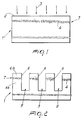
- a silicon wafer 1 is subjected to ion implanting on its entire surface 2 with low-mass inert ions 3, advantageously helium.
- Implanting occurs with relatively high helium doses which vary according to the implanting energy. For example, for an implanting energy of 20 KeV the dose is on the order of approximately 5 x 10¹⁶ atoms/sq cm, whereas for an energy of 300 KeV the dose is equal to approximately 1 x 10¹⁶ atoms/sq cm.
- a high density of small helium bubbles 4 forms at the average penetration depth of the ions 3.
- Penetration depth varies according to the implanting energy: for a value of 20 KeV of the implanting energy, penetration depth is equal to 0,3 ⁇ m, whereas for an energy of 300 KeV penetration depth is equal to 1 ⁇ m.
- the silicon wafer 1 is then subjected to heat treatments at temperatures above 700 o C. These heat treatments are capable of diffusing the helium present in the bubbles 4 up to the surface 2 of the silicon wafer 1, leaving a buried layer 7 of empty cavities in the place of the bubbles 4.
- recesses or trenches 5 are formed in the silicon wafer so that they are deeper than the depth at which the cavities 4 are located.
- protruding portions 6 which are divided by the cavities 4 into an upper section 6a and a lower section 6b.
- the silicon wafer 1 is placed in an oxidation furnace (not shown).
- An oxidation furnace (not shown).
- a fast thermal oxidation system has been chosen in the present embodiment of the present invention, but the oxidation system might be different.
- the silicon wafer 1 was subjected to the flux in an oxygen-rich environment and the temperature was raised to 1000 o C for 30 minutes.
- the buried layer which contains a high density of cavities 4, is uniformly oxidized through an oxide thickness that depends on the oxidation time and temperature, as shown in figure 3.
- Oxidation of the buried silicon layer 7 is allowed by the transport of oxygen O2 through the trenches 5 and in the porous structure of the cavity 4 formed by ion implanting.
- the upper layer 6a, insulated by the oxidized buried layer 7, is of high quality, since the slight damage thereof produced by the helium ion implanting is removed during the thermal process that produces oxidation. In particular, the damage occurs in the form of point-like defects which are eliminated by the thermal treatment.
- the wafer 1 thus obtained can then be introduced in any production cycle for forming semiconductor devices.
- the method according to the present invention fully achieves the intended aim and objects.
- the method according to the present invention is simple, inexpensive, and allows to obtain high-quality material.
- the simplicity of the method arises from the fact that only a small number of processes is required: the formation of the trenches 5, the implanting of light ions 3 to form cavities 4, and oxidation. These steps can also be performed in a sequence other than the one described herein.
- the high quality of the material obtained arises from the fact that the light ions produce defects that can be easily eliminated close to the surface of the specimen.
- various light elements can be used instead of helium.
- the structure shown in figure 2 can furthermore be formed in different ways; for example, the silicon columns or protruding portions 6 can be grown on the surface of the wafer 1.
- the cavities 4 can also be formed during the oxidation process itself instead of as a separate step.
Landscapes
- Formation Of Insulating Films (AREA)
- Element Separation (AREA)
Priority Applications (4)
| Application Number | Priority Date | Filing Date | Title |
|---|---|---|---|
| DE69408671T DE69408671T2 (de) | 1994-09-23 | 1994-09-23 | Verfahren zur Herstellung begrabener Oxidschichten in einem Silizium-Wafer |
| EP94830452A EP0703608B1 (de) | 1994-09-23 | 1994-09-23 | Verfahren zur Herstellung begrabener Oxidschichten in einem Silizium-Wafer |
| US08/527,850 US5723372A (en) | 1994-09-23 | 1995-09-14 | Method and apparatus for forming buried oxide layers within silicon wafers |
| JP7243271A JP2777783B2 (ja) | 1994-09-23 | 1995-09-21 | シリコンウェハ内に埋込酸化層を形成するための方法 |
Applications Claiming Priority (1)
| Application Number | Priority Date | Filing Date | Title |
|---|---|---|---|
| EP94830452A EP0703608B1 (de) | 1994-09-23 | 1994-09-23 | Verfahren zur Herstellung begrabener Oxidschichten in einem Silizium-Wafer |
Publications (2)
| Publication Number | Publication Date |
|---|---|
| EP0703608A1 true EP0703608A1 (de) | 1996-03-27 |
| EP0703608B1 EP0703608B1 (de) | 1998-02-25 |
Family
ID=8218534
Family Applications (1)
| Application Number | Title | Priority Date | Filing Date |
|---|---|---|---|
| EP94830452A Expired - Lifetime EP0703608B1 (de) | 1994-09-23 | 1994-09-23 | Verfahren zur Herstellung begrabener Oxidschichten in einem Silizium-Wafer |
Country Status (4)
| Country | Link |
|---|---|
| US (1) | US5723372A (de) |
| EP (1) | EP0703608B1 (de) |
| JP (1) | JP2777783B2 (de) |
| DE (1) | DE69408671T2 (de) |
Cited By (1)
| Publication number | Priority date | Publication date | Assignee | Title |
|---|---|---|---|---|
| DE19750167A1 (de) * | 1997-11-12 | 1999-05-27 | Fraunhofer Ges Forschung | Verfahren zur Herstellung integrierter Schaltkreise |
Families Citing this family (4)
| Publication number | Priority date | Publication date | Assignee | Title |
|---|---|---|---|---|
| DE69430913D1 (de) * | 1994-07-25 | 2002-08-08 | Cons Ric Microelettronica | Verfahren zur lokalen Reduzierung der Ladungsträgerlebensdauer |
| US6534380B1 (en) * | 1997-07-18 | 2003-03-18 | Denso Corporation | Semiconductor substrate and method of manufacturing the same |
| US20080203484A1 (en) * | 2007-02-23 | 2008-08-28 | Infineon Technologies Ag | Field effect transistor arrangement and method of producing a field effect transistor arrangement |
| FR2942073B1 (fr) * | 2009-02-10 | 2011-04-29 | Soitec Silicon On Insulator | Procede de realisation d'une couche de cavites |
Citations (4)
| Publication number | Priority date | Publication date | Assignee | Title |
|---|---|---|---|---|
| EP0164281A1 (de) * | 1984-04-19 | 1985-12-11 | Commissariat A L'energie Atomique | Verfahren zur Herstellung einer vergrabenen Isolierschicht in einem Halbleitersubstrat durch Ionenimplantation |
| JPS61180447A (ja) * | 1985-02-05 | 1986-08-13 | Matsushita Electric Ind Co Ltd | 半導体装置の製造方法 |
| GB2211991A (en) * | 1987-10-30 | 1989-07-12 | Atomic Energy Authority Uk | Electrical isolation of regions within semiconductor bodies |
| US5372952A (en) * | 1992-04-03 | 1994-12-13 | National Semiconductor Corporation | Method for forming isolated semiconductor structures |
Family Cites Families (2)
| Publication number | Priority date | Publication date | Assignee | Title |
|---|---|---|---|---|
| US5043292A (en) * | 1990-05-31 | 1991-08-27 | National Semiconductor Corporation | Self-aligned masking for ultra-high energy implants with application to localized buried implants and insolation structures |
| FR2681472B1 (fr) * | 1991-09-18 | 1993-10-29 | Commissariat Energie Atomique | Procede de fabrication de films minces de materiau semiconducteur. |
-
1994
- 1994-09-23 DE DE69408671T patent/DE69408671T2/de not_active Expired - Fee Related
- 1994-09-23 EP EP94830452A patent/EP0703608B1/de not_active Expired - Lifetime
-
1995
- 1995-09-14 US US08/527,850 patent/US5723372A/en not_active Expired - Lifetime
- 1995-09-21 JP JP7243271A patent/JP2777783B2/ja not_active Expired - Fee Related
Patent Citations (4)
| Publication number | Priority date | Publication date | Assignee | Title |
|---|---|---|---|---|
| EP0164281A1 (de) * | 1984-04-19 | 1985-12-11 | Commissariat A L'energie Atomique | Verfahren zur Herstellung einer vergrabenen Isolierschicht in einem Halbleitersubstrat durch Ionenimplantation |
| JPS61180447A (ja) * | 1985-02-05 | 1986-08-13 | Matsushita Electric Ind Co Ltd | 半導体装置の製造方法 |
| GB2211991A (en) * | 1987-10-30 | 1989-07-12 | Atomic Energy Authority Uk | Electrical isolation of regions within semiconductor bodies |
| US5372952A (en) * | 1992-04-03 | 1994-12-13 | National Semiconductor Corporation | Method for forming isolated semiconductor structures |
Non-Patent Citations (2)
| Title |
|---|
| E.J. ZORINSKY ER AL.: "THE "ISLANDS" METHOD- A MANUFACTURABLE POROUS SILICON SOI TECHNOLOGY", INTERNATIONAL ELECTRON DEVICES MEETING 1986 DEC. 7-10 1986, 1986, NEW YORK, pages 431 - 434, XP002079454 * |
| PATENT ABSTRACTS OF JAPAN vol. 11, no. 4 (E - 468) 7 January 1987 (1987-01-07) * |
Cited By (2)
| Publication number | Priority date | Publication date | Assignee | Title |
|---|---|---|---|---|
| DE19750167A1 (de) * | 1997-11-12 | 1999-05-27 | Fraunhofer Ges Forschung | Verfahren zur Herstellung integrierter Schaltkreise |
| DE19750167B4 (de) * | 1997-11-12 | 2006-08-31 | Fraunhofer-Gesellschaft zur Förderung der angewandten Forschung e.V. | Verfahren zur Herstellung integrierter Schaltkreise |
Also Published As
| Publication number | Publication date |
|---|---|
| US5723372A (en) | 1998-03-03 |
| JPH08111453A (ja) | 1996-04-30 |
| EP0703608B1 (de) | 1998-02-25 |
| JP2777783B2 (ja) | 1998-07-23 |
| DE69408671T2 (de) | 1998-06-18 |
| DE69408671D1 (de) | 1998-04-02 |
Similar Documents
| Publication | Publication Date | Title |
|---|---|---|
| US7148124B1 (en) | Method for forming a fragile layer inside of a single crystalline substrate preferably for making silicon-on-insulator wafers | |
| US5244819A (en) | Method to getter contamination in semiconductor devices | |
| US6429104B1 (en) | Method for forming cavities in a semiconductor substrate by implanting atoms | |
| EP0558554B1 (de) | Silizium auf porösen silizium, verfahren zur herstellung und produkt | |
| US5930643A (en) | Defect induced buried oxide (DIBOX) for throughput SOI | |
| US6593173B1 (en) | Low defect density, thin-layer, SOI substrates | |
| EP0595233A2 (de) | Verfahren zur Herstellung eines Halbleiters auf Isolator | |
| JP2007335867A (ja) | ヘテロ構造内で空孔拡散を制限する方法 | |
| JPH0637288A (ja) | 高エネルギーでイオン注入し、続いて熱処理することにより製造される、深く、薄い酸化物層を備えたsoi構造 | |
| EP0703608A1 (de) | Verfahren zur Herstellung begrabener Oxidschichten in einem Silizium-Wafer | |
| US4818711A (en) | High quality oxide on an ion implanted polysilicon surface | |
| US4451303A (en) | Diffusion of aluminum | |
| JPS5918196A (ja) | 単結晶薄膜の製造方法 | |
| JPH0846161A (ja) | Soi基板及びその製造方法 | |
| JPH088250B2 (ja) | Soi基板の作成方法及び作成装置 | |
| JPH08236614A (ja) | 半導体装置の製造方法 | |
| JPH06283421A (ja) | Soi基板およびその製造方法 | |
| JPH04242958A (ja) | 半導体基板の製造方法 | |
| Nejim et al. | Preparation and Characterisation of Thin Film Simox Material | |
| JPH10256153A (ja) | 非晶質Si層の低温単結晶化法 | |
| JP2558765B2 (ja) | 半導体装置の製造方法 | |
| JP5008799B2 (ja) | Simox基板の作製方法 | |
| JPH0748514B2 (ja) | デバイスの製造方法 | |
| JPH0574729A (ja) | 半導体装置の製造方法 | |
| JPH1079356A (ja) | 半導体基板の製造方法 |
Legal Events
| Date | Code | Title | Description |
|---|---|---|---|
| PUAI | Public reference made under article 153(3) epc to a published international application that has entered the european phase |
Free format text: ORIGINAL CODE: 0009012 |
|
| 17P | Request for examination filed |
Effective date: 19950427 |
|
| AK | Designated contracting states |
Kind code of ref document: A1 Designated state(s): DE FR GB IT |
|
| GRAG | Despatch of communication of intention to grant |
Free format text: ORIGINAL CODE: EPIDOS AGRA |
|
| GRAG | Despatch of communication of intention to grant |
Free format text: ORIGINAL CODE: EPIDOS AGRA |
|
| GRAH | Despatch of communication of intention to grant a patent |
Free format text: ORIGINAL CODE: EPIDOS IGRA |
|
| GRAH | Despatch of communication of intention to grant a patent |
Free format text: ORIGINAL CODE: EPIDOS IGRA |
|
| GRAA | (expected) grant |
Free format text: ORIGINAL CODE: 0009210 |
|
| AK | Designated contracting states |
Kind code of ref document: B1 Designated state(s): DE FR GB IT |
|
| REF | Corresponds to: |
Ref document number: 69408671 Country of ref document: DE Date of ref document: 19980402 |
|
| ITF | It: translation for a ep patent filed | ||
| ET | Fr: translation filed | ||
| PLBE | No opposition filed within time limit |
Free format text: ORIGINAL CODE: 0009261 |
|
| STAA | Information on the status of an ep patent application or granted ep patent |
Free format text: STATUS: NO OPPOSITION FILED WITHIN TIME LIMIT |
|
| 26N | No opposition filed | ||
| REG | Reference to a national code |
Ref country code: GB Ref legal event code: IF02 |
|
| PGFP | Annual fee paid to national office [announced via postgrant information from national office to epo] |
Ref country code: DE Payment date: 20031002 Year of fee payment: 10 |
|
| PGFP | Annual fee paid to national office [announced via postgrant information from national office to epo] |
Ref country code: FR Payment date: 20040908 Year of fee payment: 11 |
|
| PGFP | Annual fee paid to national office [announced via postgrant information from national office to epo] |
Ref country code: GB Payment date: 20040922 Year of fee payment: 11 |
|
| PG25 | Lapsed in a contracting state [announced via postgrant information from national office to epo] |
Ref country code: DE Free format text: LAPSE BECAUSE OF NON-PAYMENT OF DUE FEES Effective date: 20050401 |
|
| PG25 | Lapsed in a contracting state [announced via postgrant information from national office to epo] |
Ref country code: IT Free format text: LAPSE BECAUSE OF NON-PAYMENT OF DUE FEES;WARNING: LAPSES OF ITALIAN PATENTS WITH EFFECTIVE DATE BEFORE 2007 MAY HAVE OCCURRED AT ANY TIME BEFORE 2007. THE CORRECT EFFECTIVE DATE MAY BE DIFFERENT FROM THE ONE RECORDED. Effective date: 20050923 Ref country code: GB Free format text: LAPSE BECAUSE OF NON-PAYMENT OF DUE FEES Effective date: 20050923 |
|
| GBPC | Gb: european patent ceased through non-payment of renewal fee |
Effective date: 20050923 |
|
| PG25 | Lapsed in a contracting state [announced via postgrant information from national office to epo] |
Ref country code: FR Free format text: LAPSE BECAUSE OF NON-PAYMENT OF DUE FEES Effective date: 20060531 |
|
| REG | Reference to a national code |
Ref country code: FR Ref legal event code: ST Effective date: 20060531 |