EP0703611A1 - Méthode d'isolation de conducteurs métalliques, utilisant un matériau à faible constante diélectrique, et structures ainsi formées - Google Patents
Méthode d'isolation de conducteurs métalliques, utilisant un matériau à faible constante diélectrique, et structures ainsi formées Download PDFInfo
- Publication number
- EP0703611A1 EP0703611A1 EP95113563A EP95113563A EP0703611A1 EP 0703611 A1 EP0703611 A1 EP 0703611A1 EP 95113563 A EP95113563 A EP 95113563A EP 95113563 A EP95113563 A EP 95113563A EP 0703611 A1 EP0703611 A1 EP 0703611A1
- Authority
- EP
- European Patent Office
- Prior art keywords
- dielectric constant
- metal leads
- oxide
- low
- leads
- Prior art date
- Legal status (The legal status is an assumption and is not a legal conclusion. Google has not performed a legal analysis and makes no representation as to the accuracy of the status listed.)
- Granted
Links
Images


Classifications
-
- H—ELECTRICITY
- H10—SEMICONDUCTOR DEVICES; ELECTRIC SOLID-STATE DEVICES NOT OTHERWISE PROVIDED FOR
- H10P—GENERIC PROCESSES OR APPARATUS FOR THE MANUFACTURE OR TREATMENT OF DEVICES COVERED BY CLASS H10
- H10P14/00—Formation of materials, e.g. in the shape of layers or pillars
- H10P14/60—Formation of materials, e.g. in the shape of layers or pillars of insulating materials
- H10P14/68—Organic materials, e.g. photoresists
- H10P14/683—Organic materials, e.g. photoresists carbon-based polymeric organic materials, e.g. polyimides, poly cyclobutene or PVC
-
- H—ELECTRICITY
- H10—SEMICONDUCTOR DEVICES; ELECTRIC SOLID-STATE DEVICES NOT OTHERWISE PROVIDED FOR
- H10P—GENERIC PROCESSES OR APPARATUS FOR THE MANUFACTURE OR TREATMENT OF DEVICES COVERED BY CLASS H10
- H10P14/00—Formation of materials, e.g. in the shape of layers or pillars
- H10P14/60—Formation of materials, e.g. in the shape of layers or pillars of insulating materials
- H10P14/63—Formation of materials, e.g. in the shape of layers or pillars of insulating materials characterised by the formation processes
- H10P14/6326—Deposition processes
- H10P14/6342—Liquid deposition, e.g. spin-coating, sol-gel techniques or spray coating
-
- H—ELECTRICITY
- H10—SEMICONDUCTOR DEVICES; ELECTRIC SOLID-STATE DEVICES NOT OTHERWISE PROVIDED FOR
- H10P—GENERIC PROCESSES OR APPARATUS FOR THE MANUFACTURE OR TREATMENT OF DEVICES COVERED BY CLASS H10
- H10P14/00—Formation of materials, e.g. in the shape of layers or pillars
- H10P14/60—Formation of materials, e.g. in the shape of layers or pillars of insulating materials
- H10P14/65—Formation of materials, e.g. in the shape of layers or pillars of insulating materials characterised by treatments performed before or after the formation of the materials
- H10P14/6502—Formation of materials, e.g. in the shape of layers or pillars of insulating materials characterised by treatments performed before or after the formation of the materials of treatments performed before formation of the materials
- H10P14/6506—Formation of intermediate materials
-
- H—ELECTRICITY
- H10—SEMICONDUCTOR DEVICES; ELECTRIC SOLID-STATE DEVICES NOT OTHERWISE PROVIDED FOR
- H10P—GENERIC PROCESSES OR APPARATUS FOR THE MANUFACTURE OR TREATMENT OF DEVICES COVERED BY CLASS H10
- H10P14/00—Formation of materials, e.g. in the shape of layers or pillars
- H10P14/60—Formation of materials, e.g. in the shape of layers or pillars of insulating materials
- H10P14/65—Formation of materials, e.g. in the shape of layers or pillars of insulating materials characterised by treatments performed before or after the formation of the materials
- H10P14/6516—Formation of materials, e.g. in the shape of layers or pillars of insulating materials characterised by treatments performed before or after the formation of the materials of treatments performed after formation of the materials
- H10P14/6548—Formation of materials, e.g. in the shape of layers or pillars of insulating materials characterised by treatments performed before or after the formation of the materials of treatments performed after formation of the materials by forming intermediate materials, e.g. capping layers or diffusion barriers
-
- H—ELECTRICITY
- H10—SEMICONDUCTOR DEVICES; ELECTRIC SOLID-STATE DEVICES NOT OTHERWISE PROVIDED FOR
- H10P—GENERIC PROCESSES OR APPARATUS FOR THE MANUFACTURE OR TREATMENT OF DEVICES COVERED BY CLASS H10
- H10P14/00—Formation of materials, e.g. in the shape of layers or pillars
- H10P14/60—Formation of materials, e.g. in the shape of layers or pillars of insulating materials
- H10P14/69—Inorganic materials
- H10P14/692—Inorganic materials composed of oxides, glassy oxides or oxide-based glasses
- H10P14/6921—Inorganic materials composed of oxides, glassy oxides or oxide-based glasses containing silicon
- H10P14/6922—Inorganic materials composed of oxides, glassy oxides or oxide-based glasses containing silicon the material containing Si, O and at least one of H, N, C, F or other non-metal elements, e.g. SiOC, SiOC:H or SiONC
- H10P14/6926—Inorganic materials composed of oxides, glassy oxides or oxide-based glasses containing silicon the material containing Si, O and at least one of H, N, C, F or other non-metal elements, e.g. SiOC, SiOC:H or SiONC the material comprising alkyl silsesquioxane, e.g. MSQ
-
- H—ELECTRICITY
- H10—SEMICONDUCTOR DEVICES; ELECTRIC SOLID-STATE DEVICES NOT OTHERWISE PROVIDED FOR
- H10W—GENERIC PACKAGES, INTERCONNECTIONS, CONNECTORS OR OTHER CONSTRUCTIONAL DETAILS OF DEVICES COVERED BY CLASS H10
- H10W20/00—Interconnections in chips, wafers or substrates
- H10W20/01—Manufacture or treatment
- H10W20/071—Manufacture or treatment of dielectric parts thereof
- H10W20/072—Manufacture or treatment of dielectric parts thereof of dielectric parts comprising air gaps
-
- H—ELECTRICITY
- H10—SEMICONDUCTOR DEVICES; ELECTRIC SOLID-STATE DEVICES NOT OTHERWISE PROVIDED FOR
- H10W—GENERIC PACKAGES, INTERCONNECTIONS, CONNECTORS OR OTHER CONSTRUCTIONAL DETAILS OF DEVICES COVERED BY CLASS H10
- H10W20/00—Interconnections in chips, wafers or substrates
- H10W20/01—Manufacture or treatment
- H10W20/071—Manufacture or treatment of dielectric parts thereof
- H10W20/098—Manufacture or treatment of dielectric parts thereof by filling between adjacent conductive parts
-
- H—ELECTRICITY
- H10—SEMICONDUCTOR DEVICES; ELECTRIC SOLID-STATE DEVICES NOT OTHERWISE PROVIDED FOR
- H10W—GENERIC PACKAGES, INTERCONNECTIONS, CONNECTORS OR OTHER CONSTRUCTIONAL DETAILS OF DEVICES COVERED BY CLASS H10
- H10W20/00—Interconnections in chips, wafers or substrates
- H10W20/40—Interconnections external to wafers or substrates, e.g. back-end-of-line [BEOL] metallisations or vias connecting to gate electrodes
- H10W20/41—Interconnections external to wafers or substrates, e.g. back-end-of-line [BEOL] metallisations or vias connecting to gate electrodes characterised by their conductive parts
- H10W20/425—Barrier, adhesion or liner layers
-
- H—ELECTRICITY
- H10—SEMICONDUCTOR DEVICES; ELECTRIC SOLID-STATE DEVICES NOT OTHERWISE PROVIDED FOR
- H10W—GENERIC PACKAGES, INTERCONNECTIONS, CONNECTORS OR OTHER CONSTRUCTIONAL DETAILS OF DEVICES COVERED BY CLASS H10
- H10W20/00—Interconnections in chips, wafers or substrates
- H10W20/40—Interconnections external to wafers or substrates, e.g. back-end-of-line [BEOL] metallisations or vias connecting to gate electrodes
- H10W20/45—Interconnections external to wafers or substrates, e.g. back-end-of-line [BEOL] metallisations or vias connecting to gate electrodes characterised by their insulating parts
- H10W20/46—Interconnections external to wafers or substrates, e.g. back-end-of-line [BEOL] metallisations or vias connecting to gate electrodes characterised by their insulating parts comprising air gaps
-
- H—ELECTRICITY
- H10—SEMICONDUCTOR DEVICES; ELECTRIC SOLID-STATE DEVICES NOT OTHERWISE PROVIDED FOR
- H10W—GENERIC PACKAGES, INTERCONNECTIONS, CONNECTORS OR OTHER CONSTRUCTIONAL DETAILS OF DEVICES COVERED BY CLASS H10
- H10W20/00—Interconnections in chips, wafers or substrates
- H10W20/40—Interconnections external to wafers or substrates, e.g. back-end-of-line [BEOL] metallisations or vias connecting to gate electrodes
- H10W20/495—Capacitive arrangements or effects of, or between wiring layers
-
- H—ELECTRICITY
- H10—SEMICONDUCTOR DEVICES; ELECTRIC SOLID-STATE DEVICES NOT OTHERWISE PROVIDED FOR
- H10W—GENERIC PACKAGES, INTERCONNECTIONS, CONNECTORS OR OTHER CONSTRUCTIONAL DETAILS OF DEVICES COVERED BY CLASS H10
- H10W20/00—Interconnections in chips, wafers or substrates
- H10W20/01—Manufacture or treatment
- H10W20/071—Manufacture or treatment of dielectric parts thereof
- H10W20/074—Manufacture or treatment of dielectric parts thereof of dielectric parts comprising thin functional dielectric layers, e.g. dielectric etch-stop, barrier, capping or liner layers
- H10W20/077—Manufacture or treatment of dielectric parts thereof of dielectric parts comprising thin functional dielectric layers, e.g. dielectric etch-stop, barrier, capping or liner layers on sidewalls or on top surfaces of conductors
Definitions
- This invention relates generally to the fabrication of semiconductor devices, and more specifically to semiconductors having low-dielectric constant materials between leads.
- Semiconductors are widely used in integrated circuits for electronic applications, including radios and televisions. Such integrated circuits typically use multiple transistors fabricated in single crystal silicon. Many integrated circuits now contain multiple levels of metallization for interconnections.
- Semiconductor devices are being scaled down in the horizontal dimension to reduce wafer costs by obtaining more chips per wafer or by increasing circuit complexity by obtaining more transistors per chip.
- metal interconnects to semiconductor devices are not generally being scaled down in the vertical dimension (because the current density would exceed reliability limits).
- these tall metal leads are being packed closer and closer together, increasing the aspect ratio (defined as the ratio of conductor height to conductor width) to greater than one and causing capacitive coupling between the leads to become the primary limitation to circuit speed. If line-to-line capacitance is high, both circuit functionality and speed may be compromised. Reducing the capacitance within these multilevel metallization systems will reduce the RC time constant between the lines.
- the material used to isolate metal leads from each other has been silicon dioxide; however, the dielectric constant of silicon dioxide deposited by chemical vapor deposition is on the order of 4.1 to 4.2.
- the dielectric constant is based on a scale where 1.0 represents the dielectric constant of a vacuum.
- Various materials exhibit dielectric constants from very near 1.0 to values in the hundreds.
- low-dielectric constant materials to replace silicon dioxide as a dielectric material.
- the use of low-dielectric constant materials as insulating layers reduces the capacitance between metal leads, thus reducing the RC time constant. It has been found that using materials with dielectric constants of less than about 3.5 sufficiently reduces the RC time constant in typical submicron circuits.
- the term low-dielectric constant will refer to a material with a dielectric constant of less than about 3.5.
- One problem recognized herein is the difficulty of applying low-dielectric constant materials between metal leads along the entire height of the metal lead. It is desirable to have low-dielectric constant material extend the entire height of the metal leads to fully achieve the benefit of the low-dielectric constant material.
- depositing low-dielectric constant materials may involve an etchback step during which the low-dielectric constant material is removed from the tops of the leads. In some cases, portions of low-dielectric constant material are also removed from the sides of the leads as well.
- the present invention solves this problem by providing an oxide liner on top of the metal leads in order to increase the height of the low-dielectric constant material between the metal leads.
- One embodiment of the present invention is a method for insulating metal leads on a semiconductor wafer, comprising the steps of depositing a metal layer on a substrate, forming at least two metal leads on said metal layer, forming an oxide liner on said metal leads, said oxide liner having a greater thickness on the said top surface than on the side surfaces of the metal leads, and depositing a low-dielectric constant material over said oxide liner at least between said metal leads.
- a further embodiment is a semiconductor device comprising a plurality of metal leads formed on a substrate, an oxide liner formed on said metal leads, said oxide liner having a greater thickness on top surface of said metal leads than on side surfaces, and a low-dielectric constant material formed over said oxide liner at least between said metal leads.
- An advantage of the invention includes a reduction in capacitance between the metal leads.
- An oxide liner, first oxide over-layer, or both, resides on the metal leads, resulting in an increased height of the low-dielectric constant material on the metal leads. This allows the low-dielectric constant material to extend beyond the top of the metal leads, providing for an increase in process margin and decreasing the fringing capacitance and the line-to-line capacitance of the metal leads.
- oxide liner is thinner on the sides of the leads than on the tops of the leads.
- the reduced sidewall oxide thickness allows more low-dielectric constant material to be placed between metal leads, thereby reducing the line-to-line capacitance.
- Another advantage of the invention is that vias to underlying metal leads may be formed through a structurally sound and high quality dielectric material, so that traditional via formation processes can be utilized.
- Trilayer of TiN/AlCu/TiN Metal layer Other trilayers such as TiW/AlCu/TiW; Alloys of Al, Cu, Mo, W, Ti, Si; Polysilicon, silicides, nitrides, carbides.
- 116 Same as element 114 Metal leads Typically 2:1 (height:width) aspect ratio for 0.35 ⁇ m devices 118 CVD oxide Oxide liner Other suitable rigid dielectric applied thicker on tops of metal leads than on sides of metal leads.
- Parylene or polysilsequioxane Low-dielectric constant material Other types of spin-on glass; other vapor deposited polymer dielectrics such as teflon and polyimide; aerogel; air gap (inert gases or vacuum).
- TEOS SiO2 First oxide over-layer Oxide, nitride, dense glass, solid inorganic, solid organics, or other suitable rigid dielectric.
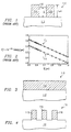
- the analysis shown in Figure 2 is for metal leads 114 having a width of 0.3 ⁇ m, spacing between leads of 0.3 ⁇ m, a thickness of 1.0 ⁇ m, and a material between leads with a dielectric constant of 2.0.
- the total capacitance of a metal lead, C T is the line-to-ground capacitance C l-g added to the line-to-line capacitance C l-l (plus cross-over capacitance).
- the line-to-ground capacitance C l-g is relatively constant; in the computer simulation of Figure 2 it is approximately 0.2 x 10 ⁇ 16 F/ ⁇ m. For closely spaced, e.g.
- C l-l 1.064 T S T + 2H T + 2H + 0.5S 0.695 + w w + 0.8S 1.4148 T + 2H T + 2H + 0.5S 0.804 + 0.831 w w + 0.8S 0.055 2H 2H + 0.5S 3.542
- ⁇ dielectric permittivity, or dielectric constant
- W width of the metal line or metal lead
- T thickness of the metal line
- H thickness of dielectric layer between metal layers
- S clear spacing between parallel lines.
- the graph shown in Figure 2 demonstrates that the higher the height of the low-dielectric constant material 120, the lower the line-to-line capacitance C l-l , and thus the lower the total capacitance C T .
- increasing the thickness of the dielectric layer (the low-dielectric constant material) from 0.5 ⁇ m to 1.0 ⁇ m decreases the capacitance by a factor of approximately 20%.
- the present invention decreases line-to-line capacitance by increasing the height, or thickness, of the low-dielectric constant material between the leads.
- Figure 3 shows a semiconductor wafer 110 having a substrate 112 which may, for example, contain transistors, diodes, and other semiconductor elements (not shown) as are well known in the art.
- the substrate 112 may also contain metal layers.
- Metal layer 114 has been deposited over the substrate 112.
- Metal layer 114 preferably comprises a trilayer of TiN/AlCu/TiN.
- the TiN is sputtered on at 200°C at a thickness of 500 angstroms.
- the aluminum copper alloy is preferably a mixture of 99 to 99.5% aluminum and 0.5 to 1.0% copper.
- the AlCu is also sputtered on at a temperature of between 100 and 200°C at a thickness of 6000 angstroms.
- Metal layer 114 is patterned and etched (e.g. by depositing a resist, patterning and exposing the resist, and then etching the metal layer) to form metal leads 116.
- the aspect ratio of the metal leads is 2:1 or higher for 0.35 ⁇ m devices and beyond (devices where the spacing between leads is 0.35 ⁇ m or less).
- the substrate 112 is eroded slightly, e.g. by 1000 ⁇ , as shown in Figure 4.
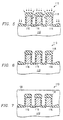
- oxide liner 118 is deposited over metal leads 116 and exposed portions of substrate 112 via a CVD oxide deposition, preferably PETEOS (plasma-enhanced tetraethoxysilane) in a nitrogen ambient.
- a CVD oxide deposition preferably PETEOS (plasma-enhanced tetraethoxysilane) in a nitrogen ambient.
- the PETEOS deposition typically is performed at a susceptor (not shown) temperature of 400 to 440°C.
- the oxide liner 118 is thicker on the tops of metal leads 116 than on the sides of the metal leads.
- the plasma decomposes TEOS into SiO2 precursors, and the nitrogen reduces the mobility of CVD SiO2 precursors.
- low-dielectric constant material 120 is deposited over the oxide liner 118, as shown in Figure 7.
- spin-on glass e.g. polysilsequioxane
- Low-dielectric constant material 120 is etched back, e.g. with a timed etch using a standard oxide etch mixture at 100 to 200°C, as shown in Figure 8.
- the low-dielectric constant material 120 remains between metal leads 116 along the entire height of the metal leads 116 or greater.
- subsequent processing steps are performed; for example, the deposition of a second oxide over-layer 126, e.g. TEOS SiO2, as shown in Figure 9.
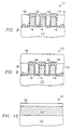
- Figure 10 shows a semiconductor wafer 110 that has a substrate 112 and a metal layer 114 deposited over substrate 112.
- a first oxide over-layer 122 is deposited over metal layer 114, as shown in Figure 10.
- both the first oxide over-layer 122 and the metal layer 114 are patterned and etched to form metal leads 116, with portions 124 of first oxide over-layer remaining on top of the metal leads 116.
- the substrate 112 is etched slightly as shown in Figure 11.
- low-dielectric constant material 120 is deposited over the portions 124 of first oxide over-layer, the sides of metal leads 116, and the exposed portions of the substrate 112, as shown in Figure 12.
- the low-dielectric constant material 120 is comprised of parylene which is highly conformal. When applied, at e.g. -70°C to room temperature, the parylene is distributed evenly over the surface of the wafer as shown in Figure 12. The parylene forms a homogeneous layer as shown in Figure 13. Next, the parylene is etched with an end point detection etch, e.g. an anisotropic oxygen plasma etch (see European patent application No: 95106830.3 filed 5/5/95 by Jeng), stopping when portions 124 of the first oxide over-layer are exposed, as shown in Figure 14. The low-dielectric constant material 120 remains between the top of the metal leads 116 and the top of the portions 124 of the first oxide over-layer. The portions 124 of the first oxide over-layer thus provide a margin for overetch of the low-dielectric constant material. Finally, subsequent processing steps may be performed, such as the deposition of a second oxide over-layer 126, as shown in Figure 15.
- an end point detection etch e.g.
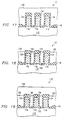
- a third embodiment of the present invention is shown in Figures 16 to 19. Beginning with the structure shown in Figure 11, an oxide liner 118 is deposited over portions 124 of first oxide over-layer, sides of metal leads 116, and exposed portions of the substrate 112, as shown in Figure 16. Next, low-dielectric constant material 120 is deposited over oxide liner 118, as shown in Figure 17. Then the low-dielectric constant material 120, preferably organic spin-on glass, is etched back, for example, with a timed etch to a height below the top of the oxide liner 118 as shown in Figure 18. This structure provides the highest process margin since there is a double layer of oxide on top of metal leads 116: portions 124 of first oxide over-layer and oxide liner 118. Again, subsequent processing steps may be performed, for example, the deposition of a second oxide over-layer 126, as shown in Figure 19.
- Table 1 indicates various preferred materials and alternates.
- the materials discussed for each embodiment are interchangeable: e.g. parylene may be used for the low-dielectric constant material in the first and third embodiments, and conversely, organic spin-on glass may be used as the low-dielectric constant material in the second embodiment.
- the deposition method described in the first embodiment may be used to form an air gap, in which the low-dielectric constant material would be an inert gas or vacuum, and no etchback of the low-dielectric constant material would be required. Depositing thinner oxide on the sides of the metal leads than on the tops of the metal leads, as described in the present invention, is also beneficial when no etchback step is performed.
- the oxide layer (oxide liner 118 in the first embodiment; portions 124 of first oxide over-layer in the second embodiment; and both the portions 124 of first oxide over-layer and oxide liner 118 in the third embodiment) allows for increased process margin during etchback of the low-dielectric constant material. This allows the formation of a thicker layer of low-dielectric constant material 120 between the metal leads 116, and thus reduces both fringing and line-to-line capacitance. The thinner portions of oxide layer on the sides of the metal leads 116 also prevent hillock formation on the sides of the metal leads 116.
- oxide liner 118 is thinner on the sides of the leads than on the tops of the leads.
- the reduced sidewall oxide thickness allows more low-dielectric constant material 120 to be placed between metal leads 116, thereby reducing the line-to-line capacitance.
- vias to underlying metal leads may be formed through a structurally sound and high quality dielectric material (e.g. second oxide over-layer 126), so that traditional via formation processes can be utilized.
- a structurally sound and high quality dielectric material e.g. second oxide over-layer 126
Landscapes
- Internal Circuitry In Semiconductor Integrated Circuit Devices (AREA)
- Formation Of Insulating Films (AREA)
Applications Claiming Priority (2)
| Application Number | Priority Date | Filing Date | Title |
|---|---|---|---|
| US29880794A | 1994-08-31 | 1994-08-31 | |
| US298807 | 1994-08-31 |
Publications (2)
| Publication Number | Publication Date |
|---|---|
| EP0703611A1 true EP0703611A1 (fr) | 1996-03-27 |
| EP0703611B1 EP0703611B1 (fr) | 2007-05-02 |
Family
ID=23152078
Family Applications (1)
| Application Number | Title | Priority Date | Filing Date |
|---|---|---|---|
| EP95113563A Expired - Lifetime EP0703611B1 (fr) | 1994-08-31 | 1995-08-29 | Méthode d'isolation de conducteurs métalliques, utilisant un matériau à faible constante diélectrique, et structures ainsi formées |
Country Status (4)
| Country | Link |
|---|---|
| US (1) | US5814558A (fr) |
| EP (1) | EP0703611B1 (fr) |
| JP (1) | JPH08107149A (fr) |
| DE (1) | DE69535488T2 (fr) |
Cited By (6)
| Publication number | Priority date | Publication date | Assignee | Title |
|---|---|---|---|---|
| WO1997047038A1 (fr) * | 1996-06-05 | 1997-12-11 | Advanced Micro Devices, Inc. | Circuit integre possedant des lignes d'interconnexion decalees verticalement et horizontalement |
| EP0834916A3 (fr) * | 1996-10-07 | 1998-07-29 | Motorola, Inc. | Méthode de formation d'une structure semiconductrice comprenant des regions formées par un matériau à constante diélectrique faible |
| EP0851471A3 (fr) * | 1996-12-25 | 1999-06-09 | Nec Corporation | Dispositif semiconducteur avec deux isolants de constante diéléctrique différentes et son procédé de fabrication |
| EP1005087A1 (fr) * | 1998-11-26 | 2000-05-31 | STMicroelectronics SA | Circuit intégré et procédé de fabrication associé |
| EP0905778A3 (fr) * | 1997-09-29 | 2001-02-07 | Siemens Aktiengesellschaft | Structure conductrice améliorée à plusieurs niveaux et procédé de fabrication |
| EP1119035A3 (fr) * | 2000-01-18 | 2005-06-08 | Applied Materials, Inc. | Méthode de dépôt d'une couche diélectrique à faible constant diélectrique |
Families Citing this family (12)
| Publication number | Priority date | Publication date | Assignee | Title |
|---|---|---|---|---|
| JP2773729B2 (ja) * | 1996-02-29 | 1998-07-09 | 日本電気株式会社 | 半導体装置の製造方法 |
| JPH10335458A (ja) | 1997-05-30 | 1998-12-18 | Nec Corp | 半導体装置及びその製造方法 |
| JP3102382B2 (ja) * | 1997-05-30 | 2000-10-23 | 日本電気株式会社 | 半導体装置およびその製造方法 |
| US6444564B1 (en) * | 1998-11-23 | 2002-09-03 | Advanced Micro Devices, Inc. | Method and product for improved use of low k dielectric material among integrated circuit interconnect structures |
| US6734564B1 (en) * | 1999-01-04 | 2004-05-11 | International Business Machines Corporation | Specially shaped contact via and integrated circuit therewith |
| US6071805A (en) * | 1999-01-25 | 2000-06-06 | Chartered Semiconductor Manufacturing, Ltd. | Air gap formation for high speed IC processing |
| US6436814B1 (en) | 2000-11-21 | 2002-08-20 | International Business Machines Corporation | Interconnection structure and method for fabricating same |
| US6432811B1 (en) * | 2000-12-20 | 2002-08-13 | Intel Corporation | Method of forming structural reinforcement of highly porous low k dielectric films by Cu diffusion barrier structures |
| US7446047B2 (en) * | 2005-02-18 | 2008-11-04 | Taiwan Semiconductor Manufacturing Company, Ltd. | Metal structure with sidewall passivation and method |
| JP4827639B2 (ja) * | 2006-07-12 | 2011-11-30 | ルネサスエレクトロニクス株式会社 | 半導体装置およびその製造方法 |
| US8456009B2 (en) | 2010-02-18 | 2013-06-04 | Taiwan Semiconductor Manufacturing Company, Ltd. | Semiconductor structure having an air-gap region and a method of manufacturing the same |
| US9449871B1 (en) | 2015-11-18 | 2016-09-20 | International Business Machines Corporation | Hybrid airgap structure with oxide liner |
Citations (5)
| Publication number | Priority date | Publication date | Assignee | Title |
|---|---|---|---|---|
| EP0411795A1 (fr) * | 1989-07-31 | 1991-02-06 | AT&T Corp. | Depôt anisotrope de dioxyde de silicium |
| EP0476625A2 (fr) * | 1990-09-18 | 1992-03-25 | Nec Corporation | Dispositif semi-conducteur comprenant des interconnexions |
| US5155576A (en) * | 1990-03-28 | 1992-10-13 | Nec Corporation | Semiconductor integrated circuit having a multilayer wiring structure |
| US5310700A (en) * | 1993-03-26 | 1994-05-10 | Integrated Device Technology, Inc. | Conductor capacitance reduction in integrated circuits |
| EP0660409A1 (fr) * | 1993-12-14 | 1995-06-28 | AT&T GLOBAL INFORMATION SOLUTIONS INTERNATIONAL INC. | Procédé pour la fabrication des circuits integrés |
Family Cites Families (15)
| Publication number | Priority date | Publication date | Assignee | Title |
|---|---|---|---|---|
| US4986878A (en) * | 1988-07-19 | 1991-01-22 | Cypress Semiconductor Corp. | Process for improved planarization of the passivation layers for semiconductor devices |
| KR910008980B1 (ko) * | 1988-12-20 | 1991-10-26 | 현대전자산업 주식회사 | 자외선을 이용한 s.o.g 박막 경화 방법 |
| EP0393635B1 (fr) * | 1989-04-21 | 1997-09-03 | Nec Corporation | Dispositif semi-conducteur comprenant des conducteurs multicouche |
| JPH0437067A (ja) * | 1990-05-31 | 1992-02-07 | Canon Inc | 半導体素子用電極及び該電極を有する半導体装置及びその製造方法 |
| US5231043A (en) * | 1991-08-21 | 1993-07-27 | Sgs-Thomson Microelectronics, Inc. | Contact alignment for integrated circuits |
| JPH05267290A (ja) * | 1992-03-18 | 1993-10-15 | Nec Yamaguchi Ltd | 半導体集積回路およびその製造方法 |
| EP0572704B1 (fr) * | 1992-06-05 | 2000-04-19 | Semiconductor Process Laboratory Co., Ltd. | Procédé de fabrication d'un dispositif semi-conducteur comportant une méthode de réforme d'une couche isolante obtenue par CVD à basse température |
| US5302233A (en) * | 1993-03-19 | 1994-04-12 | Micron Semiconductor, Inc. | Method for shaping features of a semiconductor structure using chemical mechanical planarization (CMP) |
| US5366850A (en) * | 1993-04-14 | 1994-11-22 | Industrial Technology Research Institute | Submicron planarization process with passivation on metal line |
| US5403780A (en) * | 1993-06-04 | 1995-04-04 | Jain; Vivek | Method enhancing planarization etchback margin, reliability, and stability of a semiconductor device |
| US5641711A (en) * | 1994-04-28 | 1997-06-24 | Texas Instruments Incorporated | Low dielectric constant insulation in VLSI applications |
| US5407860A (en) * | 1994-05-27 | 1995-04-18 | Texas Instruments Incorporated | Method of forming air gap dielectric spaces between semiconductor leads |
| US5461003A (en) * | 1994-05-27 | 1995-10-24 | Texas Instruments Incorporated | Multilevel interconnect structure with air gaps formed between metal leads |
| US5476817A (en) * | 1994-05-31 | 1995-12-19 | Texas Instruments Incorporated | Method of making reliable metal leads in high speed LSI semiconductors using both dummy leads and thermoconductive layers |
| US5413962A (en) * | 1994-07-15 | 1995-05-09 | United Microelectronics Corporation | Multi-level conductor process in VLSI fabrication utilizing an air bridge |
-
1995
- 1995-08-29 EP EP95113563A patent/EP0703611B1/fr not_active Expired - Lifetime
- 1995-08-29 DE DE69535488T patent/DE69535488T2/de not_active Expired - Lifetime
- 1995-08-31 JP JP7224016A patent/JPH08107149A/ja active Pending
-
1996
- 1996-06-04 US US08/658,401 patent/US5814558A/en not_active Expired - Lifetime
Patent Citations (5)
| Publication number | Priority date | Publication date | Assignee | Title |
|---|---|---|---|---|
| EP0411795A1 (fr) * | 1989-07-31 | 1991-02-06 | AT&T Corp. | Depôt anisotrope de dioxyde de silicium |
| US5155576A (en) * | 1990-03-28 | 1992-10-13 | Nec Corporation | Semiconductor integrated circuit having a multilayer wiring structure |
| EP0476625A2 (fr) * | 1990-09-18 | 1992-03-25 | Nec Corporation | Dispositif semi-conducteur comprenant des interconnexions |
| US5310700A (en) * | 1993-03-26 | 1994-05-10 | Integrated Device Technology, Inc. | Conductor capacitance reduction in integrated circuits |
| EP0660409A1 (fr) * | 1993-12-14 | 1995-06-28 | AT&T GLOBAL INFORMATION SOLUTIONS INTERNATIONAL INC. | Procédé pour la fabrication des circuits integrés |
Non-Patent Citations (4)
| Title |
|---|
| GRETCHEN M ADEMA ET AL: "PASSIVATION SCHEMES FOR COPPER/POLYMER THIN FILM INTERCONNECTIONS USED IN MULTICHIP MODULES", PROCEEDINGS OF THE ELECTRONIC COMPONENTS AND TECHNOLOGY CONFERENCE (ECTC), SAN DIEGO, MAY 18 - 20, 1992, no. CONF. 42, 18 May 1992 (1992-05-18) - 20 May 1992 (1992-05-20), INSTITUTE OF ELECTRICAL AND ELECTRONICS ENGINEERS, pages 776 - 782, XP000474031 * |
| GREWAL V ET AL: "A NOVEL MULTILEVEL METALLIZATION TECHNIQUE FOR ADVANCED CMOS AND BIPOLAR INTEGRATED CIRCUITS", IEEE VLSI MULTILEVEL INTERCONNECTION CONFERENCE, SANTA CLARA, JUNE 9 - 10, 1986, INSTITUTE OF ELECTRICAL AND ELECTRONICS ENGINEERS, pages 107 - 113, XP000010154 * |
| JOEL R. WIESNER: "Gap filling of multilevel metal interconnects with 0.25 micrometer geometries", SOLID STATE TECHNOLOGY, vol. 36, no. 10, WASHINGTON US, pages 63 - 64, XP000440193 * |
| SHIN-PUU JENG ET AL: "A planarized multilevel interconnect scheme with embedded low-dielectric-constant polymers for sub-quarter-micron applications", 1994 SYMPOSIUM ON VLSI TECHNOLOGY. DIGEST OF TECHNICAL PAPERS (CAT. NO.94CH3433-0), PROCEEDINGS OF 1994 VLSI TECHNOLOGY SYMPOSIUM, HONOLULU, HI, USA, 7-9 JUNE 1994, ISBN 0-7803-1921-4, 1994, NEW YORK, NY, USA, IEEE, USA, pages 73 - 74 * |
Cited By (19)
| Publication number | Priority date | Publication date | Assignee | Title |
|---|---|---|---|---|
| US6153833A (en) * | 1996-06-05 | 2000-11-28 | Advanced Micro Devices, Inc. | Integrated circuit having interconnect lines separated by a dielectric having a capping layer |
| US5854131A (en) * | 1996-06-05 | 1998-12-29 | Advanced Micro Devices, Inc. | Integrated circuit having horizontally and vertically offset interconnect lines |
| WO1997047038A1 (fr) * | 1996-06-05 | 1997-12-11 | Advanced Micro Devices, Inc. | Circuit integre possedant des lignes d'interconnexion decalees verticalement et horizontalement |
| EP0834916A3 (fr) * | 1996-10-07 | 1998-07-29 | Motorola, Inc. | Méthode de formation d'une structure semiconductrice comprenant des regions formées par un matériau à constante diélectrique faible |
| US5880018A (en) * | 1996-10-07 | 1999-03-09 | Motorola Inc. | Method for manufacturing a low dielectric constant inter-level integrated circuit structure |
| EP0851471A3 (fr) * | 1996-12-25 | 1999-06-09 | Nec Corporation | Dispositif semiconducteur avec deux isolants de constante diéléctrique différentes et son procédé de fabrication |
| EP0905778A3 (fr) * | 1997-09-29 | 2001-02-07 | Siemens Aktiengesellschaft | Structure conductrice améliorée à plusieurs niveaux et procédé de fabrication |
| KR100544030B1 (ko) * | 1997-09-29 | 2007-03-02 | 지멘스 악티엔게젤샤프트 | 다중-레벨도전구조물및그의제조방법 |
| FR2786609A1 (fr) * | 1998-11-26 | 2000-06-02 | St Microelectronics Sa | Circuit integre a capacite interlignes reduite et procede de fabrication associe |
| EP1005087A1 (fr) * | 1998-11-26 | 2000-05-31 | STMicroelectronics SA | Circuit intégré et procédé de fabrication associé |
| US6392299B1 (en) | 1998-11-26 | 2002-05-21 | Stmicroelectronics S.A. | Integrated circuit and associated fabrication process |
| EP1119035A3 (fr) * | 2000-01-18 | 2005-06-08 | Applied Materials, Inc. | Méthode de dépôt d'une couche diélectrique à faible constant diélectrique |
| US7012030B2 (en) | 2000-01-18 | 2006-03-14 | Applied Materials Inc. | Very low dielectric constant plasma-enhanced CVD films |
| US7094710B2 (en) | 2000-01-18 | 2006-08-22 | Applied Materials | Very low dielectric constant plasma-enhanced CVD films |
| US7205224B2 (en) | 2000-01-18 | 2007-04-17 | Applied Materials, Inc. | Very low dielectric constant plasma-enhanced CVD films |
| US7399697B2 (en) | 2000-01-18 | 2008-07-15 | Applied Materials, Inc. | Very low dielectric constant plasma-enhanced CVD films |
| US7601631B2 (en) | 2000-01-18 | 2009-10-13 | Appplied Materials, Inc. | Very low dielectric constant plasma-enhanced CVD films |
| US7633163B2 (en) | 2000-01-18 | 2009-12-15 | Applied Materials, Inc. | Very low dielectric constant plasma-enhanced CVD films |
| US7825042B2 (en) | 2000-01-18 | 2010-11-02 | Applied Materials, Inc. | Very low dielectric constant plasma-enhanced CVD films |
Also Published As
| Publication number | Publication date |
|---|---|
| JPH08107149A (ja) | 1996-04-23 |
| EP0703611B1 (fr) | 2007-05-02 |
| DE69535488T2 (de) | 2008-01-03 |
| US5814558A (en) | 1998-09-29 |
| DE69535488D1 (de) | 2007-06-14 |
Similar Documents
| Publication | Publication Date | Title |
|---|---|---|
| EP0703611B1 (fr) | Méthode d'isolation de conducteurs métalliques, utilisant un matériau à faible constante diélectrique, et structures ainsi formées | |
| EP0687005B1 (fr) | Procédé de fabrication d'interconnections sur des dispositifs semiconducteurs | |
| US5828121A (en) | Multi-level conduction structure for VLSI circuits | |
| EP0689246B1 (fr) | Améliorations concernant des dispositifs semi-conducteurs | |
| US6174808B1 (en) | Intermetal dielectric using HDP-CVD oxide and SACVD O3-TEOS | |
| US6177329B1 (en) | Integrated circuit structures having gas pockets and method for forming integrated circuit structures having gas pockets | |
| US5453157A (en) | Low temperature anisotropic ashing of resist for semiconductor fabrication | |
| US5461003A (en) | Multilevel interconnect structure with air gaps formed between metal leads | |
| US7119441B2 (en) | Semiconductor interconnect structure | |
| US6072689A (en) | Ferroelectric capacitor and integrated circuit device comprising same | |
| CN101366116B (zh) | 制造厚布线结构的双镶嵌工艺 | |
| US5432128A (en) | Reliability enhancement of aluminum interconnects by reacting aluminum leads with a strengthening gas | |
| US5674771A (en) | Capacitor and method of manufacturing the same | |
| US7009272B2 (en) | PECVD air gap integration | |
| JPH05235184A (ja) | 半導体装置の多層配線構造体の製造方法 | |
| US6191031B1 (en) | Process for producing multi-layer wiring structure | |
| EP1743366B1 (fr) | Structure de cablage pour circuit integre a capacite intercouche reduite | |
| US6103639A (en) | Method of reducing pin holes in a nitride passivation layer | |
| US5498571A (en) | Method of manufacturing a semiconductor device having reliable multi-layered wiring | |
| US6100590A (en) | Low capacitance multilevel metal interconnect structure and method of manufacture | |
| CN1221017C (zh) | 改进的氟掺杂二氧化硅薄膜 | |
| EP0864175B1 (fr) | Nouvelle technologie de passivation de parois laterales avec metallisation pour des applications sur circuits integres a des profondeurs inferieures au demi-micron | |
| US6133628A (en) | Metal layer interconnects with improved performance characteristics | |
| US6472312B2 (en) | Methods for inhibiting microelectronic damascene processing induced low dielectric constant dielectric layer physical degradation | |
| US5554884A (en) | Multilevel metallization process for use in fabricating microelectronic devices |
Legal Events
| Date | Code | Title | Description |
|---|---|---|---|
| PUAI | Public reference made under article 153(3) epc to a published international application that has entered the european phase |
Free format text: ORIGINAL CODE: 0009012 |
|
| AK | Designated contracting states |
Kind code of ref document: A1 Designated state(s): DE FR GB IT NL |
|
| 17P | Request for examination filed |
Effective date: 19960912 |
|
| 17Q | First examination report despatched |
Effective date: 20010329 |
|
| GRAP | Despatch of communication of intention to grant a patent |
Free format text: ORIGINAL CODE: EPIDOSNIGR1 |
|
| GRAS | Grant fee paid |
Free format text: ORIGINAL CODE: EPIDOSNIGR3 |
|
| GRAA | (expected) grant |
Free format text: ORIGINAL CODE: 0009210 |
|
| AK | Designated contracting states |
Kind code of ref document: B1 Designated state(s): DE FR GB IT NL |
|
| REG | Reference to a national code |
Ref country code: GB Ref legal event code: FG4D |
|
| REF | Corresponds to: |
Ref document number: 69535488 Country of ref document: DE Date of ref document: 20070614 Kind code of ref document: P |
|
| ET | Fr: translation filed | ||
| NLV1 | Nl: lapsed or annulled due to failure to fulfill the requirements of art. 29p and 29m of the patents act | ||
| PG25 | Lapsed in a contracting state [announced via postgrant information from national office to epo] |
Ref country code: NL Free format text: LAPSE BECAUSE OF FAILURE TO SUBMIT A TRANSLATION OF THE DESCRIPTION OR TO PAY THE FEE WITHIN THE PRESCRIBED TIME-LIMIT Effective date: 20070502 |
|
| PLBE | No opposition filed within time limit |
Free format text: ORIGINAL CODE: 0009261 |
|
| STAA | Information on the status of an ep patent application or granted ep patent |
Free format text: STATUS: NO OPPOSITION FILED WITHIN TIME LIMIT |
|
| 26N | No opposition filed |
Effective date: 20080205 |
|
| PG25 | Lapsed in a contracting state [announced via postgrant information from national office to epo] |
Ref country code: IT Free format text: LAPSE BECAUSE OF FAILURE TO SUBMIT A TRANSLATION OF THE DESCRIPTION OR TO PAY THE FEE WITHIN THE PRESCRIBED TIME-LIMIT Effective date: 20070502 |
|
| PGFP | Annual fee paid to national office [announced via postgrant information from national office to epo] |
Ref country code: FR Payment date: 20090806 Year of fee payment: 15 |
|
| PGFP | Annual fee paid to national office [announced via postgrant information from national office to epo] |
Ref country code: DE Payment date: 20100831 Year of fee payment: 16 |
|
| PGFP | Annual fee paid to national office [announced via postgrant information from national office to epo] |
Ref country code: GB Payment date: 20100708 Year of fee payment: 16 |
|
| REG | Reference to a national code |
Ref country code: FR Ref legal event code: ST Effective date: 20110502 |
|
| PG25 | Lapsed in a contracting state [announced via postgrant information from national office to epo] |
Ref country code: FR Free format text: LAPSE BECAUSE OF NON-PAYMENT OF DUE FEES Effective date: 20100831 |
|
| GBPC | Gb: european patent ceased through non-payment of renewal fee |
Effective date: 20110829 |
|
| REG | Reference to a national code |
Ref country code: DE Ref legal event code: R119 Ref document number: 69535488 Country of ref document: DE Effective date: 20120301 |
|
| PG25 | Lapsed in a contracting state [announced via postgrant information from national office to epo] |
Ref country code: GB Free format text: LAPSE BECAUSE OF NON-PAYMENT OF DUE FEES Effective date: 20110829 |
|
| PG25 | Lapsed in a contracting state [announced via postgrant information from national office to epo] |
Ref country code: DE Free format text: LAPSE BECAUSE OF NON-PAYMENT OF DUE FEES Effective date: 20120301 |