EP0704743A1 - Méthode de traitement pour aligner des molécules de cristal liquide et dispositif d'affichage à cristal liquide - Google Patents
Méthode de traitement pour aligner des molécules de cristal liquide et dispositif d'affichage à cristal liquide Download PDFInfo
- Publication number
- EP0704743A1 EP0704743A1 EP95115079A EP95115079A EP0704743A1 EP 0704743 A1 EP0704743 A1 EP 0704743A1 EP 95115079 A EP95115079 A EP 95115079A EP 95115079 A EP95115079 A EP 95115079A EP 0704743 A1 EP0704743 A1 EP 0704743A1
- Authority
- EP
- European Patent Office
- Prior art keywords
- liquid crystal
- crystal molecules
- film
- treating method
- aligning
- Prior art date
- Legal status (The legal status is an assumption and is not a legal conclusion. Google has not performed a legal analysis and makes no representation as to the accuracy of the status listed.)
- Granted
Links
- 238000000034 method Methods 0.000 title claims abstract description 56
- 239000004973 liquid crystal related substance Substances 0.000 title claims abstract description 49
- 229920001721 polyimide Polymers 0.000 claims abstract description 58
- 239000000758 substrate Substances 0.000 claims abstract description 27
- 239000007788 liquid Substances 0.000 claims abstract description 19
- 238000009826 distribution Methods 0.000 claims abstract description 8
- 125000000962 organic group Chemical group 0.000 claims abstract description 7
- 230000001678 irradiating effect Effects 0.000 claims abstract description 4
- SECXISVLQFMRJM-UHFFFAOYSA-N N-Methylpyrrolidone Chemical compound CN1CCCC1=O SECXISVLQFMRJM-UHFFFAOYSA-N 0.000 claims description 15
- ZMXDDKWLCZADIW-UHFFFAOYSA-N N,N-Dimethylformamide Chemical compound CN(C)C=O ZMXDDKWLCZADIW-UHFFFAOYSA-N 0.000 claims description 12
- YEJRWHAVMIAJKC-UHFFFAOYSA-N 4-Butyrolactone Chemical compound O=C1CCCO1 YEJRWHAVMIAJKC-UHFFFAOYSA-N 0.000 claims description 8
- 125000002029 aromatic hydrocarbon group Chemical group 0.000 claims description 7
- IAZDPXIOMUYVGZ-UHFFFAOYSA-N Dimethylsulphoxide Chemical compound CS(C)=O IAZDPXIOMUYVGZ-UHFFFAOYSA-N 0.000 claims description 6
- SWXVUIWOUIDPGS-UHFFFAOYSA-N diacetone alcohol Chemical compound CC(=O)CC(C)(C)O SWXVUIWOUIDPGS-UHFFFAOYSA-N 0.000 claims description 6
- FXHOOIRPVKKKFG-UHFFFAOYSA-N N,N-Dimethylacetamide Chemical compound CN(C)C(C)=O FXHOOIRPVKKKFG-UHFFFAOYSA-N 0.000 claims description 4
- XLLIQLLCWZCATF-UHFFFAOYSA-N ethylene glycol monomethyl ether acetate Natural products COCCOC(C)=O XLLIQLLCWZCATF-UHFFFAOYSA-N 0.000 claims description 4
- 125000005647 linker group Chemical group 0.000 claims description 4
- XNWFRZJHXBZDAG-UHFFFAOYSA-N 2-METHOXYETHANOL Chemical compound COCCO XNWFRZJHXBZDAG-UHFFFAOYSA-N 0.000 claims description 3
- 125000003118 aryl group Chemical group 0.000 claims description 3
- CYSGHNMQYZDMIA-UHFFFAOYSA-N 1,3-Dimethyl-2-imidazolidinon Chemical compound CN1CCN(C)C1=O CYSGHNMQYZDMIA-UHFFFAOYSA-N 0.000 claims description 2
- SBASXUCJHJRPEV-UHFFFAOYSA-N 2-(2-methoxyethoxy)ethanol Chemical compound COCCOCCO SBASXUCJHJRPEV-UHFFFAOYSA-N 0.000 claims description 2
- ZNQVEEAIQZEUHB-UHFFFAOYSA-N 2-ethoxyethanol Chemical compound CCOCCO ZNQVEEAIQZEUHB-UHFFFAOYSA-N 0.000 claims description 2
- XXJWXESWEXIICW-UHFFFAOYSA-N diethylene glycol monoethyl ether Chemical compound CCOCCOCCO XXJWXESWEXIICW-UHFFFAOYSA-N 0.000 claims description 2
- 229940075557 diethylene glycol monoethyl ether Drugs 0.000 claims description 2
- 239000003495 polar organic solvent Substances 0.000 claims description 2
- RUOJZAUFBMNUDX-UHFFFAOYSA-N propylene carbonate Chemical compound CC1COC(=O)O1 RUOJZAUFBMNUDX-UHFFFAOYSA-N 0.000 claims description 2
- 239000004642 Polyimide Substances 0.000 description 26
- 239000002904 solvent Substances 0.000 description 11
- 229920005575 poly(amic acid) Polymers 0.000 description 6
- 239000002243 precursor Substances 0.000 description 5
- 238000000576 coating method Methods 0.000 description 4
- 239000011521 glass Substances 0.000 description 4
- QSHDDOUJBYECFT-UHFFFAOYSA-N mercury Chemical compound [Hg] QSHDDOUJBYECFT-UHFFFAOYSA-N 0.000 description 4
- 229910052753 mercury Inorganic materials 0.000 description 4
- 239000011248 coating agent Substances 0.000 description 3
- 230000000052 comparative effect Effects 0.000 description 3
- 238000000206 photolithography Methods 0.000 description 3
- KMKWGXGSGPYISJ-UHFFFAOYSA-N 4-[4-[2-[4-(4-aminophenoxy)phenyl]propan-2-yl]phenoxy]aniline Chemical compound C=1C=C(OC=2C=CC(N)=CC=2)C=CC=1C(C)(C)C(C=C1)=CC=C1OC1=CC=C(N)C=C1 KMKWGXGSGPYISJ-UHFFFAOYSA-N 0.000 description 2
- YGYCECQIOXZODZ-UHFFFAOYSA-N 4415-87-6 Chemical compound O=C1OC(=O)C2C1C1C(=O)OC(=O)C12 YGYCECQIOXZODZ-UHFFFAOYSA-N 0.000 description 2
- 239000004677 Nylon Substances 0.000 description 2
- JUJWROOIHBZHMG-UHFFFAOYSA-N Pyridine Chemical compound C1=CC=NC=C1 JUJWROOIHBZHMG-UHFFFAOYSA-N 0.000 description 2
- 150000004984 aromatic diamines Chemical class 0.000 description 2
- 230000015572 biosynthetic process Effects 0.000 description 2
- 210000004027 cell Anatomy 0.000 description 2
- 238000004140 cleaning Methods 0.000 description 2
- 230000007547 defect Effects 0.000 description 2
- 150000004985 diamines Chemical class 0.000 description 2
- KZTYYGOKRVBIMI-UHFFFAOYSA-N diphenyl sulfone Chemical compound C=1C=CC=CC=1S(=O)(=O)C1=CC=CC=C1 KZTYYGOKRVBIMI-UHFFFAOYSA-N 0.000 description 2
- 239000004744 fabric Substances 0.000 description 2
- 229920001778 nylon Polymers 0.000 description 2
- 239000003960 organic solvent Substances 0.000 description 2
- 238000006068 polycondensation reaction Methods 0.000 description 2
- 239000009719 polyimide resin Substances 0.000 description 2
- HHVIBTZHLRERCL-UHFFFAOYSA-N sulfonyldimethane Chemical compound CS(C)(=O)=O HHVIBTZHLRERCL-UHFFFAOYSA-N 0.000 description 2
- XLYOFNOQVPJJNP-UHFFFAOYSA-N water Substances O XLYOFNOQVPJJNP-UHFFFAOYSA-N 0.000 description 2
- AVQQQNCBBIEMEU-UHFFFAOYSA-N 1,1,3,3-tetramethylurea Chemical compound CN(C)C(=O)N(C)C AVQQQNCBBIEMEU-UHFFFAOYSA-N 0.000 description 1
- HLBLWEWZXPIGSM-UHFFFAOYSA-N 4-Aminophenyl ether Chemical compound C1=CC(N)=CC=C1OC1=CC=C(N)C=C1 HLBLWEWZXPIGSM-UHFFFAOYSA-N 0.000 description 1
- JCRRFJIVUPSNTA-UHFFFAOYSA-N 4-[4-(4-aminophenoxy)phenoxy]aniline Chemical compound C1=CC(N)=CC=C1OC(C=C1)=CC=C1OC1=CC=C(N)C=C1 JCRRFJIVUPSNTA-UHFFFAOYSA-N 0.000 description 1
- 0 CC1=COC(C2O*OC22)C2O1 Chemical compound CC1=COC(C2O*OC22)C2O1 0.000 description 1
- 229920000742 Cotton Polymers 0.000 description 1
- MQJKPEGWNLWLTK-UHFFFAOYSA-N Dapsone Chemical compound C1=CC(N)=CC=C1S(=O)(=O)C1=CC=C(N)C=C1 MQJKPEGWNLWLTK-UHFFFAOYSA-N 0.000 description 1
- ZWXPDGCFMMFNRW-UHFFFAOYSA-N N-methylcaprolactam Chemical compound CN1CCCCCC1=O ZWXPDGCFMMFNRW-UHFFFAOYSA-N 0.000 description 1
- 239000004988 Nematic liquid crystal Substances 0.000 description 1
- 229920003171 Poly (ethylene oxide) Polymers 0.000 description 1
- 239000004962 Polyamide-imide Substances 0.000 description 1
- 239000004372 Polyvinyl alcohol Substances 0.000 description 1
- VYPSYNLAJGMNEJ-UHFFFAOYSA-N Silicium dioxide Chemical compound O=[Si]=O VYPSYNLAJGMNEJ-UHFFFAOYSA-N 0.000 description 1
- 239000004990 Smectic liquid crystal Substances 0.000 description 1
- 230000005260 alpha ray Effects 0.000 description 1
- 229930188620 butyrolactone Natural products 0.000 description 1
- 210000002858 crystal cell Anatomy 0.000 description 1
- 230000018044 dehydration Effects 0.000 description 1
- 238000006297 dehydration reaction Methods 0.000 description 1
- 238000007598 dipping method Methods 0.000 description 1
- 230000005611 electricity Effects 0.000 description 1
- 238000010894 electron beam technology Methods 0.000 description 1
- 239000005262 ferroelectric liquid crystals (FLCs) Substances 0.000 description 1
- 230000005669 field effect Effects 0.000 description 1
- 238000010438 heat treatment Methods 0.000 description 1
- 125000005842 heteroatom Chemical group 0.000 description 1
- GNOIPBMMFNIUFM-UHFFFAOYSA-N hexamethylphosphoric triamide Chemical compound CN(C)P(=O)(N(C)C)N(C)C GNOIPBMMFNIUFM-UHFFFAOYSA-N 0.000 description 1
- 150000003949 imides Chemical class 0.000 description 1
- 238000007654 immersion Methods 0.000 description 1
- 238000004519 manufacturing process Methods 0.000 description 1
- 239000011159 matrix material Substances 0.000 description 1
- 239000000203 mixture Substances 0.000 description 1
- 125000001997 phenyl group Chemical group [H]C1=C([H])C([H])=C(*)C([H])=C1[H] 0.000 description 1
- 230000010287 polarization Effects 0.000 description 1
- 229920002312 polyamide-imide Polymers 0.000 description 1
- 229920000728 polyester Polymers 0.000 description 1
- 238000006116 polymerization reaction Methods 0.000 description 1
- -1 polyoxyethylene Polymers 0.000 description 1
- 229920002451 polyvinyl alcohol Polymers 0.000 description 1
- 238000003825 pressing Methods 0.000 description 1
- 238000007639 printing Methods 0.000 description 1
- UMJSCPRVCHMLSP-UHFFFAOYSA-N pyridine Natural products COC1=CC=CN=C1 UMJSCPRVCHMLSP-UHFFFAOYSA-N 0.000 description 1
- 238000006798 ring closing metathesis reaction Methods 0.000 description 1
- 239000004065 semiconductor Substances 0.000 description 1
- 229910052814 silicon oxide Inorganic materials 0.000 description 1
- 239000007787 solid Substances 0.000 description 1
- 125000006850 spacer group Chemical group 0.000 description 1
- 238000005507 spraying Methods 0.000 description 1
- 230000003068 static effect Effects 0.000 description 1
- 239000000126 substance Substances 0.000 description 1
- 229920001169 thermoplastic Polymers 0.000 description 1
- 239000004416 thermosoftening plastic Substances 0.000 description 1
- 238000002834 transmittance Methods 0.000 description 1
- 238000007740 vapor deposition Methods 0.000 description 1
- 229910052724 xenon Inorganic materials 0.000 description 1
- FHNFHKCVQCLJFQ-UHFFFAOYSA-N xenon atom Chemical compound [Xe] FHNFHKCVQCLJFQ-UHFFFAOYSA-N 0.000 description 1
Images

Classifications
-
- G—PHYSICS
- G02—OPTICS
- G02F—OPTICAL DEVICES OR ARRANGEMENTS FOR THE CONTROL OF LIGHT BY MODIFICATION OF THE OPTICAL PROPERTIES OF THE MEDIA OF THE ELEMENTS INVOLVED THEREIN; NON-LINEAR OPTICS; FREQUENCY-CHANGING OF LIGHT; OPTICAL LOGIC ELEMENTS; OPTICAL ANALOGUE/DIGITAL CONVERTERS
- G02F1/00—Devices or arrangements for the control of the intensity, colour, phase, polarisation or direction of light arriving from an independent light source, e.g. switching, gating or modulating; Non-linear optics
- G02F1/01—Devices or arrangements for the control of the intensity, colour, phase, polarisation or direction of light arriving from an independent light source, e.g. switching, gating or modulating; Non-linear optics for the control of the intensity, phase, polarisation or colour
- G02F1/13—Devices or arrangements for the control of the intensity, colour, phase, polarisation or direction of light arriving from an independent light source, e.g. switching, gating or modulating; Non-linear optics for the control of the intensity, phase, polarisation or colour based on liquid crystals, e.g. single liquid crystal display cells
- G02F1/133—Constructional arrangements; Operation of liquid crystal cells; Circuit arrangements
- G02F1/1333—Constructional arrangements; Manufacturing methods
- G02F1/1337—Surface-induced orientation of the liquid crystal molecules, e.g. by alignment layers
- G02F1/133711—Surface-induced orientation of the liquid crystal molecules, e.g. by alignment layers by organic films, e.g. polymeric films
- G02F1/133723—Polyimide, polyamide-imide
-
- G—PHYSICS
- G02—OPTICS
- G02F—OPTICAL DEVICES OR ARRANGEMENTS FOR THE CONTROL OF LIGHT BY MODIFICATION OF THE OPTICAL PROPERTIES OF THE MEDIA OF THE ELEMENTS INVOLVED THEREIN; NON-LINEAR OPTICS; FREQUENCY-CHANGING OF LIGHT; OPTICAL LOGIC ELEMENTS; OPTICAL ANALOGUE/DIGITAL CONVERTERS
- G02F1/00—Devices or arrangements for the control of the intensity, colour, phase, polarisation or direction of light arriving from an independent light source, e.g. switching, gating or modulating; Non-linear optics
- G02F1/01—Devices or arrangements for the control of the intensity, colour, phase, polarisation or direction of light arriving from an independent light source, e.g. switching, gating or modulating; Non-linear optics for the control of the intensity, phase, polarisation or colour
- G02F1/13—Devices or arrangements for the control of the intensity, colour, phase, polarisation or direction of light arriving from an independent light source, e.g. switching, gating or modulating; Non-linear optics for the control of the intensity, phase, polarisation or colour based on liquid crystals, e.g. single liquid crystal display cells
- G02F1/133—Constructional arrangements; Operation of liquid crystal cells; Circuit arrangements
- G02F1/1333—Constructional arrangements; Manufacturing methods
- G02F1/1337—Surface-induced orientation of the liquid crystal molecules, e.g. by alignment layers
-
- C—CHEMISTRY; METALLURGY
- C09—DYES; PAINTS; POLISHES; NATURAL RESINS; ADHESIVES; COMPOSITIONS NOT OTHERWISE PROVIDED FOR; APPLICATIONS OF MATERIALS NOT OTHERWISE PROVIDED FOR
- C09K—MATERIALS FOR MISCELLANEOUS APPLICATIONS, NOT PROVIDED FOR ELSEWHERE
- C09K2323/00—Functional layers of liquid crystal optical display excluding electroactive liquid crystal layer characterised by chemical composition
- C09K2323/02—Alignment layer characterised by chemical composition
- C09K2323/027—Polyimide
Definitions
- the present invention relates to a treating method for aligning liquid crystal molecules and a liquid crystal display device employing it. More particularly, it relates to a treating method for aligning liquid crystal molecules, which is capable of aligning liquid crystal molecules without rubbing treatment and which is excellent in the productivity from the industrial viewpoint, and a liquid crystal display device employing it.
- a liquid crystal display device is a display device utilizing an electrooptical change of liquid crystal, and as a device, it is small in size and light in weight and has a characteristic such that the power consumption is small. By virtue of such characteristics, it has been developed remarkably in recent years as a display device for various displays.
- a twisted nematic type (TN type) field-effect liquid crystal display device is a typical example, wherein nematic liquid crystal having a positive dielectric anisotropy is used, and liquid crystal molecules are aligned in parallel with substrates at the respective interfaces of the opposing pair of electrode substrates, and the two substrates are assembled so that the aligning directions of the liquid crystal molecules are mutually perpendicular to each other.
- TN type twisted nematic type
- the first method is a method wherein an inorganic substance such as silicon oxide is vapor-deposited obliquely on a substrate to form an inorganic film on the substrate, so that the liquid crystal molecules are aligned in the direction of vapor-deposition.
- the second method is a method wherein an organic coating film is formed on a substrate surface, and its surface is rubbed in a certain direction with a cloth of e.g. cotton, nylon, polyester or the like, so that the liquid crystal molecules will be aligned in the rubbing direction.
- a cloth of e.g. cotton, nylon, polyester or the like e.g. cotton, nylon, polyester or the like.
- this method is most commonly employed for the industrial purpose.
- the organic film polyvinyl alcohol, polyoxyethylene, polyamide or polyimide may, for example, be mentioned.
- polyimide which is chemically and thermally most excellent, is commonly used from the viewpoint such that it has sufficient stability and durability for industrial mass production.
- the treating method for alignment by rubbing polyimide was an industrially useful method which is simple and excellent in the productivity.
- a STN (supertwisted nematic) system wherein the twist angle of the TN type liquid crystal display device has increased
- an AM (active matrix) system wherein switching elements are formed for individual electrodes, respectively
- a FLC (ferroelectric) system employing ferroelectric liquid crystal and an AFLC (antiferroelectric) system employing antiferroelectric liquid crystal may, for example, be mentioned.
- a so-called "rubbingless" alignment method has been studied for aligning liquid crystal molecules without rubbing, and various methods have been proposed.
- a method wherein photochromic molecules are introduced to the surface of the alignment film so that the molecules at the surface of the alignment film are aligned by light Japanese Unexamined Patent Publication No. 2844/1992
- a method wherein a LB film (a Langmuir ⁇ Blodgett film) is used to align molecular chains constituting the alignment film Japanese Unexamined Patent Publication No. 2844/1992
- a method wherein a LB film a Langmuir ⁇ Blodgett film
- a photolithography method may be mentioned as an efficient method for forming periodical convexes and concaves on the surface of a highly reliable polyimide film.
- Polyimide is used as an insulating film for semiconductors by virtue of the excellent electrical characteristics and the high insulating property.
- a so-called photosensitive polyimide has been developed, whereby the polyimide itself has a photocurable property.
- This is an attempt to form periodical concaves and convexes by a photolithography method employing such a photocurable polyimide.
- concaves and convexes can surely be formed on the surface of the polyimide film.
- this photocurable polyimide has essentially be developed as an insulating film.
- the present invention has been made to solve these problems, and it is an object of the present invention to provide a method for alignment treatment by an industrially useful method which is simple and excellent in productivity, and a liquid crystal display device employing it.
- the present invention provides a treating method for aligning liquid crystal molecules, which comprises forming on a substrate a polyimide film represented by a repeating unit of the formula (I): wherein R is a bivalent organic group, irradiating the film with ultraviolet rays having a spatial distribution of irradiation intensity through a mask, immersing it in a developing liquid and then in a rinsing liquid to form periodical concaves and convexes on the surface of the polyimide film, and aligning liquid crystal molecules on the concave-convex surface.
- a treating method for aligning liquid crystal molecules which comprises forming on a substrate a polyimide film represented by a repeating unit of the formula (I): wherein R is a bivalent organic group, irradiating the film with ultraviolet rays having a spatial distribution of irradiation intensity through a mask, immersing it in a developing liquid and then in a rinsing liquid to form periodical concaves and convexes
- the present invention provides a liquid crystal display device having liquid crystal sandwiched between a pair of substrates having electrodes formed thereon, wherein on at least one of the substrates, a polyimide film represented by a repeating unit of the formula (I): wherein R is a bivalent organic group, is formed, the film is irradiated with ultraviolet rays having a spatial distribution of irradiation intensity through a mask, and then immersed in a developing liquid and then in a rinsing liquid to form periodical concaves and convexes on the surface of the polyimide film, and liquid crystal molecules are aligned on the concave-convex surface.
- a polyimide film represented by a repeating unit of the formula (I): wherein R is a bivalent organic group
- the polyimide of the formula (I) of the present invention is a polyimide which is excellent in the transparency (Japanese Examined Patent Publication No. 11615/1990 which corresponds to U.S. Patent 5,053,480), and when rubbing treatment is applied thereto, and such polyimide is used as a liquid crystal alignment film, it has excellent alignment characteristics (Japanese Examined Patent Publication No. 33010/1992). Further, it has been reported that some of polyimides having a structure of the formula (I) are capable of forming a predetermined pattern by irradiation with ultraviolet rays. (Japanese Unexamined Patent Publication No. 135449/1990 which corresponds to U.S. Patent 4,877,718)
- the polyimide of the formula (I) can be obtained by the method disclosed in Japanese Examined Patent Publication No. 11615/1990 (which corresponds to U.S. Patent 5,053,480). Namely, 1,2,3,4-cyclobutanetetracarboxylic dianhydride and a diamine are subjected to a polycondensation reaction in a solvent at an optional molar ratio of from 0.5 to 2, preferably from 0.9 to 1.1 to obtain a polyimide precursor (polyamic acid), which is converted to an imide.
- the diamine used here is usually an aromatic diamine, preferably an aromatic diamine having a hetero atom.
- diaminodiphenyl ether 1,4-bis(4-aminophenoxy)benzene, 4,4'-bis(4-aminophenoxy)diphenylsulfone, 2,2-bis[4-(4-aminophenoxy)phenyl]propane and 4,4'-diaminodiphenylsulfone may be mentioned as typical examples.
- the bivalent organic group R is an aromatic hydrocarbon group.
- the aromatic hydrocarbon group is preferably an aromatic hydrocarbon group having at least one linking group selected from the group consisting of -SO-, -S-, -SO2- ,and -O- as a linking group of an aromatic ring in the aromatic hydrocarbon group, and as the aromatic ring, a benzene ring is preferred.
- the temperature for the polycondensation reaction may be selected at an optional level from -20°C to 150°C. However, the temperature is preferably within a range of -5°C to 100°C.
- the solvent for the polymerization is not particularly limited so long as it is capable of dissolving the resulting polyamic acid. Typical examples include N,N-dimethylformamide, N,N-dimethylacetamide, N-methylpyrrolidone, N-methylcaprolactam, dimethylsulfoxide, tetramethylurea, pyridine, dimethylsulfone, hexamethylphosphoramide and butyrolactone. These solvents may be used alone or in combination as a mixture.
- a solvent which does not dissolve the polyamic acid may be added to the above solvent within a range where the polyamic acid is dissolved.
- a method for forming a polyimide film by coating the obtained polyamic acid on the substrate is carried out by the method disclosed in Japanese Examined Patent Publication No. 33010/1992. Namely, a solution of the above-mentioned polyimide precursor is coated on a substrate and then heated to remove the solvent and to subject the polyimide precursor to dehydration ring closure to form a uniform polyimide film on the substrate. This heating temperature can be selected at an optional level of from 150°C to 400°C.
- a polyimide solution may be coated as it is, and then the solvent may be evaporated to form a polyimide film.
- the coating method is not particularly limited, and a method such as dipping, coating, printing or spraying may be employed.
- the method of irradiating the polyimide film with ultraviolet rays having a spatial distribution of irradiation intensity through a mask, followed by immersing in a developing liquid and then in a rinsing liquid to form periodical concaves and convexes on the surface of the polyimide film can be carried out in accordance with a method for forming a patterned insulating layer, as shown in Japanese Unexamined Patent Publication No. 135449/1990 (which corresponds to U.S. Patent 4,877,718).
- the ultraviolet rays to be irradiated may be from any light source so long as the light source has a wavelength region of from 200 nm to 400nm, and a high pressure mercury lamp, a super high pressure mercury lamp, a xenon lamp and a DrF excimer laser may, for example, be mentioned as typical examples.
- a high pressure mercury lamp is most common taking into the industrial productivity into consideration.
- the polyimide film is irradiated with the ultraviolet rays having a spatial distribution of irradiation intensity, whereby soluble exposed regions and non-exposed regions will be formed in the film.
- the exposed regions are dissolved by a solvent and removed and cleaned to form concaves and convexes on the surface of the polyimide.
- An aprotic highly polar organic solvent is preferred as the organic solvent for dissolving and removing the exposed regions i.e. as the developing liquid.
- a solvent include N-methyl-2-pyrrolidone, N,N-dimethylformamide, N,N-dimethylacetamide, dimethylsulfoxide, 1,3-dimethyl-2-imidazolidinone, ⁇ -butyrolactone, diacetone alcohol, ethylene glycol monomethyl ether, ethylene glycol monoethyl ether, diethylene glycol monomethyl ether, diethylene glycol monoethyl ether, ethylene glycol monomethyl ether acetate and propylene carbonate.
- Particularly preferred organic solvents are N-methyl-2-pyrrolidone, N,N-dimethylformamide, N,N-dimethylacetamide, ⁇ -butyrolactone, diacetone alcohol and ethylene glycol monomethyl ether.
- rinsing liquid water is usually employed.
- the shape of the concaves and convexes on the surface of the polyimide film can be varied widely depending upon the pattern image of the mask employed, the intensity distribution of the irradiated ultraviolet rays and the developing conditions for dissolving and removing the exposed regions by means of a solvent to develop the pattern image. Further, depending upon the pattern image of the mask, periodical concaves and convexes having different directions in the same plane of the polyimide film, can be formed.
- NMP N-methylpyrrolidone
- This solution was diluted with NMP to a total solid content of 7 wt% and then spin-coated on a glass substrate of 60 mm ⁇ 70 mm ⁇ 1.2 mm at 3,500 rpm and then heat-treated at 80°C for 10 minutes and at 250°C for one hour to form a polyimide resin film having a thickness of 1 ⁇ m.
- the respective polyimide films were subjected to exposure for the period of time as identified in Table 1 by a high pressure mercury lamp with an output of 300 W through a mask for exposure wherein lines L (exposed portions) and spaces S (light-shielding portions) in slit shapes as identified in Figure 1 have pattern sizes as identified in Example 1 in Table 1.
- the substrates treated as described above, were immersed in N-methylpyrrolidone for a predetermined period of time for development and further immersed in pure water for 5 minutes for cleaning.
- the surface of such substrates was inspected by a scanning electron microscope, whereby periodical concaves and convexes as shown in Figure 2 were observed on the surface of the polyimide films.
- reference numeral 1 indicates the light-shielding portion
- numeral 2 the polyimide film
- numeral 3 the glass substrate
- symbol L the width of the light-shielding portion
- symbol S the width of the exposed portion
- symbol x the distance between adjacent convexes
- symbol y the height of the convexes.
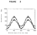
- ⁇ represents Example 1, ⁇ Example 2, ⁇ Example 3, ⁇ Example 4, ⁇ Example 5, and --- Comparative Example 1.
Landscapes
- Physics & Mathematics (AREA)
- Nonlinear Science (AREA)
- Spectroscopy & Molecular Physics (AREA)
- Mathematical Physics (AREA)
- Chemical & Material Sciences (AREA)
- Crystallography & Structural Chemistry (AREA)
- General Physics & Mathematics (AREA)
- Optics & Photonics (AREA)
- Liquid Crystal (AREA)
- Macromolecular Compounds Obtained By Forming Nitrogen-Containing Linkages In General (AREA)
Applications Claiming Priority (3)
| Application Number | Priority Date | Filing Date | Title |
|---|---|---|---|
| JP236812/94 | 1994-09-30 | ||
| JP23681294 | 1994-09-30 | ||
| JP6236812A JPH08101393A (ja) | 1994-09-30 | 1994-09-30 | 液晶配向処理方法及び液晶表示素子 |
Publications (2)
| Publication Number | Publication Date |
|---|---|
| EP0704743A1 true EP0704743A1 (fr) | 1996-04-03 |
| EP0704743B1 EP0704743B1 (fr) | 2002-11-27 |
Family
ID=17006153
Family Applications (1)
| Application Number | Title | Priority Date | Filing Date |
|---|---|---|---|
| EP95115079A Expired - Lifetime EP0704743B1 (fr) | 1994-09-30 | 1995-09-25 | Méthode de traitement pour aligner des molécules de cristal liquide et dispositif d'affichage à cristal liquide |
Country Status (6)
| Country | Link |
|---|---|
| US (1) | US5607732A (fr) |
| EP (1) | EP0704743B1 (fr) |
| JP (1) | JPH08101393A (fr) |
| KR (1) | KR960011521A (fr) |
| DE (1) | DE69528947T2 (fr) |
| TW (1) | TW420766B (fr) |
Cited By (1)
| Publication number | Priority date | Publication date | Assignee | Title |
|---|---|---|---|---|
| EP0940724A3 (fr) * | 1998-03-05 | 2000-06-07 | Hitachi Chemical DuPont MicroSystems Ltd. | Développateur pour un précurseur de polyimide photosensible et méthode pour son utilisation pour la structuration |
Families Citing this family (17)
| Publication number | Priority date | Publication date | Assignee | Title |
|---|---|---|---|---|
| JP3298607B2 (ja) * | 1995-09-29 | 2002-07-02 | ソニー株式会社 | 液晶素子及びその製造方法 |
| TW448336B (en) * | 1996-07-11 | 2001-08-01 | Nissan Chemical Ind Ltd | Alignment treating agent for a liquid crystal cell |
| US6291797B1 (en) * | 1996-08-13 | 2001-09-18 | Nippon Sheet Glass Co., Ltd. | Laser machining method for glass substrate, diffraction type optical device fabricated by the machining method, and method of manufacturing optical device |
| KR19980057654A (ko) * | 1996-12-30 | 1998-09-25 | 손욱 | 액정표시소자 및 그 제조방법 |
| KR100474780B1 (ko) * | 1997-02-07 | 2005-08-04 | 후지 샤신 필름 가부시기가이샤 | 광학보상시이트,그의제조방법및액정디스플레이 |
| JP4126731B2 (ja) | 1997-03-13 | 2008-07-30 | Jsr株式会社 | 液晶配向剤 |
| RU2123430C1 (ru) * | 1997-03-26 | 1998-12-20 | Закрытое акционерное общество "Кванта Инвест" | Декоративный материал и способ его изготовления |
| US6846522B1 (en) | 1999-09-27 | 2005-01-25 | Optiva, Inc. | Decorative material and method of its fabrication |
| JP2002196337A (ja) | 2000-09-06 | 2002-07-12 | Seiko Epson Corp | 電気光学装置の製造方法及び製造装置、並びに液晶パネルの製造方法及び製造装置 |
| JP4334166B2 (ja) * | 2001-08-01 | 2009-09-30 | シャープ株式会社 | 液晶表示装置及び配向膜の露光装置及び配向膜の処理方法 |
| US20050068476A1 (en) * | 2003-05-26 | 2005-03-31 | Masato Okabe | Polarizing plate, liquid crystal display using the same and method for manufacturing polarizing plate |
| JP4517624B2 (ja) * | 2003-10-09 | 2010-08-04 | セイコーエプソン株式会社 | 液晶表示装置、液晶表示装置の製造方法、電子機器 |
| JP5116287B2 (ja) * | 2005-11-21 | 2013-01-09 | 株式会社ジャパンディスプレイイースト | 液晶表示装置 |
| KR100792134B1 (ko) * | 2006-01-04 | 2008-01-04 | 주식회사 엘지화학 | 액정 배향용 조성물, 이로 제조된 액정 배향막, 및 이를포함하는 액정 디스플레이 |
| KR101184069B1 (ko) * | 2006-03-29 | 2012-09-19 | 엘지디스플레이 주식회사 | 폴리이미드막 도포 장치 및 그 방법 |
| KR101951507B1 (ko) * | 2011-09-15 | 2019-02-22 | 닛산 가가쿠 가부시키가이샤 | 액정 배향막의 제조 방법, 액정 배향막, 및 액정 표시 소자 |
| KR20160009159A (ko) * | 2014-07-15 | 2016-01-26 | 삼성디스플레이 주식회사 | 광배향 조성물 및 이를 이용한 표시 패널의 제조 방법 |
Citations (2)
| Publication number | Priority date | Publication date | Assignee | Title |
|---|---|---|---|---|
| JPS6147932A (ja) * | 1984-08-15 | 1986-03-08 | Nissan Chem Ind Ltd | 液晶表示素子 |
| JPH022515A (ja) * | 1988-06-16 | 1990-01-08 | Matsushita Electric Ind Co Ltd | 液晶用配向膜の製法 |
Family Cites Families (2)
| Publication number | Priority date | Publication date | Assignee | Title |
|---|---|---|---|---|
| JPS606726A (ja) * | 1983-06-25 | 1985-01-14 | Nissan Chem Ind Ltd | 新規ポリイミド樹脂及びその製造法 |
| US4877718A (en) * | 1988-09-26 | 1989-10-31 | Rennsselaer Polytechnic Institute | Positive-working photosensitive polyimide operated by photo induced molecular weight changes |
-
1994
- 1994-09-30 JP JP6236812A patent/JPH08101393A/ja active Pending
-
1995
- 1995-09-18 TW TW084109772A patent/TW420766B/zh not_active IP Right Cessation
- 1995-09-18 US US08/529,456 patent/US5607732A/en not_active Expired - Lifetime
- 1995-09-25 DE DE69528947T patent/DE69528947T2/de not_active Expired - Fee Related
- 1995-09-25 EP EP95115079A patent/EP0704743B1/fr not_active Expired - Lifetime
- 1995-09-29 KR KR1019950033155A patent/KR960011521A/ko not_active Ceased
Patent Citations (3)
| Publication number | Priority date | Publication date | Assignee | Title |
|---|---|---|---|---|
| JPS6147932A (ja) * | 1984-08-15 | 1986-03-08 | Nissan Chem Ind Ltd | 液晶表示素子 |
| JPH0433010B2 (fr) * | 1984-08-15 | 1992-06-01 | Nissan Chemical Ind Ltd | |
| JPH022515A (ja) * | 1988-06-16 | 1990-01-08 | Matsushita Electric Ind Co Ltd | 液晶用配向膜の製法 |
Non-Patent Citations (2)
| Title |
|---|
| PATENT ABSTRACTS OF JAPAN vol. 10, no. 206 (P - 478) * |
| PATENT ABSTRACTS OF JAPAN vol. 14, no. 136 (P - 1021) * |
Cited By (2)
| Publication number | Priority date | Publication date | Assignee | Title |
|---|---|---|---|---|
| EP0940724A3 (fr) * | 1998-03-05 | 2000-06-07 | Hitachi Chemical DuPont MicroSystems Ltd. | Développateur pour un précurseur de polyimide photosensible et méthode pour son utilisation pour la structuration |
| US6146815A (en) * | 1998-03-05 | 2000-11-14 | Hitachi Chemical Dupont Microsystems L.L.C. | Developer for photosensitive polyimide precursor, and method of using it for patterning |
Also Published As
| Publication number | Publication date |
|---|---|
| US5607732A (en) | 1997-03-04 |
| JPH08101393A (ja) | 1996-04-16 |
| DE69528947T2 (de) | 2003-07-03 |
| EP0704743B1 (fr) | 2002-11-27 |
| KR960011521A (ko) | 1996-04-20 |
| TW420766B (en) | 2001-02-01 |
| DE69528947D1 (de) | 2003-01-09 |
Similar Documents
| Publication | Publication Date | Title |
|---|---|---|
| EP0704743B1 (fr) | Méthode de traitement pour aligner des molécules de cristal liquide et dispositif d'affichage à cristal liquide | |
| US6063829A (en) | Method for liquid crystal alignment | |
| JP3893659B2 (ja) | 液晶配向処理方法 | |
| CN100437301C (zh) | 光取向用液晶取向剂及使用它的液晶显示元件 | |
| JP3725555B2 (ja) | 液晶においてプレチルトを誘起する方法及び液晶表示素子 | |
| KR100939628B1 (ko) | 신규한 폴리이미드 공중합체, 이를 포함하는 액정 배향막,및 이를 포함하는 액정 디스플레이 | |
| KR101610558B1 (ko) | 액정 배향제, 액정 배향막 및 액정 표시 소자 | |
| JP4207430B2 (ja) | 液晶配向剤、液晶配向膜の形成方法および液晶表示素子 | |
| CN101321845B (zh) | 制备液晶取向层的方法、采用该方法制备的液晶取向层以及包括该液晶取向层的液晶显示器 | |
| JPS6066233A (ja) | 強誘電性液晶表示素子における配列方法 | |
| US6054190A (en) | Method for producing an alignment chemisorption monomolecular film | |
| US6348245B1 (en) | Polymide photo alignment film from 3,3′,4,4′-benzophenone tetracarboxylic dianhydride and ortho-substituted aromatic diamines for liquid crystal displays | |
| EP1355971B1 (fr) | Polyimides photosensibles pour alignement optique de cristaux liquides | |
| JP3308356B2 (ja) | 液晶素子用配向膜付き基板およびその製造方法ならびに液晶素子 | |
| CN101365769A (zh) | 用于液晶取向的组合物、由该组合物制备的液晶取向层以及包含该组合物的液晶显示器 | |
| US5925423A (en) | Optical alignment polymer, alignment layer formed using the same and liquid crystal display device having the alignment layer | |
| US6793987B2 (en) | Photoalignment materials and liquid crystal display fabricated with such photoalignment materials | |
| KR100230436B1 (ko) | 광배향성 조성물, 이로부터 형성된 배향막 및이 배향막을 구비한 액정표시소자 | |
| TWI917713B (zh) | 液晶配向劑、液晶配向膜及其製造方法、以及液晶元件 | |
| JPH10148835A (ja) | 液晶配向膜 | |
| JPH0553118A (ja) | 液晶配向膜の製造方法 | |
| JP2001133742A (ja) | ポリマーを塗布された長寿命の光学メモリーデバイスの製造方法 | |
| JP2000112125A (ja) | 感光性樹脂材料、液晶用配向膜材料およびそれを用いた液晶素子 | |
| JPH0572537A (ja) | 液晶表示素子 | |
| JP2000111921A (ja) | 感光性樹脂材料、液晶用配向膜材料およびそれを用いた液晶素子 |
Legal Events
| Date | Code | Title | Description |
|---|---|---|---|
| PUAI | Public reference made under article 153(3) epc to a published international application that has entered the european phase |
Free format text: ORIGINAL CODE: 0009012 |
|
| AK | Designated contracting states |
Kind code of ref document: A1 Designated state(s): DE FR GB IT NL |
|
| 17P | Request for examination filed |
Effective date: 19960919 |
|
| 17Q | First examination report despatched |
Effective date: 20000825 |
|
| GRAG | Despatch of communication of intention to grant |
Free format text: ORIGINAL CODE: EPIDOS AGRA |
|
| GRAG | Despatch of communication of intention to grant |
Free format text: ORIGINAL CODE: EPIDOS AGRA |
|
| GRAH | Despatch of communication of intention to grant a patent |
Free format text: ORIGINAL CODE: EPIDOS IGRA |
|
| GRAH | Despatch of communication of intention to grant a patent |
Free format text: ORIGINAL CODE: EPIDOS IGRA |
|
| GRAA | (expected) grant |
Free format text: ORIGINAL CODE: 0009210 |
|
| AK | Designated contracting states |
Kind code of ref document: B1 Designated state(s): DE FR GB IT NL |
|
| REG | Reference to a national code |
Ref country code: GB Ref legal event code: FG4D |
|
| REF | Corresponds to: |
Ref document number: 69528947 Country of ref document: DE Date of ref document: 20030109 |
|
| ET | Fr: translation filed | ||
| PLBE | No opposition filed within time limit |
Free format text: ORIGINAL CODE: 0009261 |
|
| STAA | Information on the status of an ep patent application or granted ep patent |
Free format text: STATUS: NO OPPOSITION FILED WITHIN TIME LIMIT |
|
| 26N | No opposition filed |
Effective date: 20030828 |
|
| PGFP | Annual fee paid to national office [announced via postgrant information from national office to epo] |
Ref country code: FR Payment date: 20060908 Year of fee payment: 12 |
|
| PGFP | Annual fee paid to national office [announced via postgrant information from national office to epo] |
Ref country code: NL Payment date: 20060917 Year of fee payment: 12 |
|
| PGFP | Annual fee paid to national office [announced via postgrant information from national office to epo] |
Ref country code: GB Payment date: 20060920 Year of fee payment: 12 |
|
| PGFP | Annual fee paid to national office [announced via postgrant information from national office to epo] |
Ref country code: DE Payment date: 20060922 Year of fee payment: 12 |
|
| PGFP | Annual fee paid to national office [announced via postgrant information from national office to epo] |
Ref country code: IT Payment date: 20060930 Year of fee payment: 12 |
|
| GBPC | Gb: european patent ceased through non-payment of renewal fee |
Effective date: 20070925 |
|
| PG25 | Lapsed in a contracting state [announced via postgrant information from national office to epo] |
Ref country code: NL Free format text: LAPSE BECAUSE OF NON-PAYMENT OF DUE FEES Effective date: 20080401 |
|
| NLV4 | Nl: lapsed or anulled due to non-payment of the annual fee |
Effective date: 20080401 |
|
| PG25 | Lapsed in a contracting state [announced via postgrant information from national office to epo] |
Ref country code: DE Free format text: LAPSE BECAUSE OF NON-PAYMENT OF DUE FEES Effective date: 20080401 |
|
| REG | Reference to a national code |
Ref country code: FR Ref legal event code: ST Effective date: 20080531 |
|
| PG25 | Lapsed in a contracting state [announced via postgrant information from national office to epo] |
Ref country code: FR Free format text: LAPSE BECAUSE OF NON-PAYMENT OF DUE FEES Effective date: 20071001 |
|
| PG25 | Lapsed in a contracting state [announced via postgrant information from national office to epo] |
Ref country code: GB Free format text: LAPSE BECAUSE OF NON-PAYMENT OF DUE FEES Effective date: 20070925 |
|
| PG25 | Lapsed in a contracting state [announced via postgrant information from national office to epo] |
Ref country code: IT Free format text: LAPSE BECAUSE OF NON-PAYMENT OF DUE FEES Effective date: 20070925 |