EP0704904B1 - Kapazitätserzeugungsverfahren - Google Patents
Kapazitätserzeugungsverfahren Download PDFInfo
- Publication number
- EP0704904B1 EP0704904B1 EP95115448A EP95115448A EP0704904B1 EP 0704904 B1 EP0704904 B1 EP 0704904B1 EP 95115448 A EP95115448 A EP 95115448A EP 95115448 A EP95115448 A EP 95115448A EP 0704904 B1 EP0704904 B1 EP 0704904B1
- Authority
- EP
- European Patent Office
- Prior art keywords
- capacitances
- unit
- capacitance
- unit capacitances
- xij
- Prior art date
- Legal status (The legal status is an assumption and is not a legal conclusion. Google has not performed a legal analysis and makes no representation as to the accuracy of the status listed.)
- Expired - Lifetime
Links
Images


Classifications
-
- H—ELECTRICITY
- H10—SEMICONDUCTOR DEVICES; ELECTRIC SOLID-STATE DEVICES NOT OTHERWISE PROVIDED FOR
- H10D—INORGANIC ELECTRIC SEMICONDUCTOR DEVICES
- H10D84/00—Integrated devices formed in or on semiconductor substrates that comprise only semiconducting layers, e.g. on Si wafers or on GaAs-on-Si wafers
- H10D84/201—Integrated devices formed in or on semiconductor substrates that comprise only semiconducting layers, e.g. on Si wafers or on GaAs-on-Si wafers characterised by the integration of only components covered by H10D1/00 or H10D8/00, e.g. RLC circuits
- H10D84/204—Integrated devices formed in or on semiconductor substrates that comprise only semiconducting layers, e.g. on Si wafers or on GaAs-on-Si wafers characterised by the integration of only components covered by H10D1/00 or H10D8/00, e.g. RLC circuits of combinations of diodes or capacitors or resistors
- H10D84/212—Integrated devices formed in or on semiconductor substrates that comprise only semiconducting layers, e.g. on Si wafers or on GaAs-on-Si wafers characterised by the integration of only components covered by H10D1/00 or H10D8/00, e.g. RLC circuits of combinations of diodes or capacitors or resistors of only capacitors
-
- H—ELECTRICITY
- H10—SEMICONDUCTOR DEVICES; ELECTRIC SOLID-STATE DEVICES NOT OTHERWISE PROVIDED FOR
- H10D—INORGANIC ELECTRIC SEMICONDUCTOR DEVICES
- H10D84/00—Integrated devices formed in or on semiconductor substrates that comprise only semiconducting layers, e.g. on Si wafers or on GaAs-on-Si wafers
- H10D84/201—Integrated devices formed in or on semiconductor substrates that comprise only semiconducting layers, e.g. on Si wafers or on GaAs-on-Si wafers characterised by the integration of only components covered by H10D1/00 or H10D8/00, e.g. RLC circuits
- H10D84/204—Integrated devices formed in or on semiconductor substrates that comprise only semiconducting layers, e.g. on Si wafers or on GaAs-on-Si wafers characterised by the integration of only components covered by H10D1/00 or H10D8/00, e.g. RLC circuits of combinations of diodes or capacitors or resistors
- H10D84/206—Integrated devices formed in or on semiconductor substrates that comprise only semiconducting layers, e.g. on Si wafers or on GaAs-on-Si wafers characterised by the integration of only components covered by H10D1/00 or H10D8/00, e.g. RLC circuits of combinations of diodes or capacitors or resistors of combinations of capacitors and resistors
Definitions
- the present invention relates to a capacitance forming method, with a plurality of unit capacitances according to the preamble part of claim 1.
- a capacitance forming method is proposed a shown in Figure 8, wherein a plurality of predetermined unit capacitances are aligned, then some unit capacitances are selected for one capacitance component so that there is no adjacent pairs of the unit capacitances selected for the one capacitance component. The deviation of the capacitances is minimized in order to compensate the relative accuracy of capacities of capacitance components.
- capacitance components consisting of a plurality of unit capacitances are of good relative accuracy when the components have capacities nearly equal to one another.
- capacities are much different in such case that weights of digits of binary number are represented by the capacitance components.
- inequality of forming is caused due to flowing direction in the peripheral area of the alignment area of unit capacitances, and the relative accuracy becomes lower.
- JP-A-58103163 discloses a method for forming a capacitor element wherein dummy patterns are constructed in such a manner that they will be placed in a row on the circumferential part of the structure. At this location, the relative error of a weighted capacitor is less while the capacitor element occupies a small area.
- EP-A-0186239 discloses an integrated circuit comprising capacitances of different capacitance values having different numbers of basic capacitances connected in parallel between a first and second connection electrode.
- the circuit is comprised of a plurality of rows having the same number of basic capacitances and in different ones of these rows different numbers of basic capacitances form part of the said capacitances whereas all the remaining basic capacitances of the relevant rows are dummy capacitances.
- the present invention is invented so as to solve the conventional problems and to provide a capacitance method having the steps as set forth in claim 1.
- Figure 1 is a plan view showing an arrangement of unit capacitances for obtaining a capacity ratio of 8:4:2:1:1, in the arrangement the unit capacitances are aligned in a matrix of 4 ⁇ 4 unit capacitances.
- a capacity of an unit capacitance is Cu
- a capacity of a capacitance with the maximum capacity is defined as 8Cu
- capacities of the following second capacitance are defined as 4Cu, 2Cu, Cu and Cu.
- FIG 1 there are arranged the unit capacitances designated by references “a”, “b”, “c”, “d” and “e”.
- the reference “a” shows unit capacitances for a capacitance, or a capacitance component, of 8Cu (It is called the first capacitance.).
- the unit capacitances “b” are for a capacitance component of 4Cu (It is called the second capacitance.).
- the unit capacitances "c” are for a capacitance component of 2Cu (It is called the third capacitance.).
- the unit capacitances "d” are for a capacitance component of Cu (It s called the fourth capacitance.).
- the unit capacitances "e" are for a capacitance component of Cu (It is called the fifth or last capacitance.).
- the unit capacitances of the first capacitance are arranged in a checker flag.
- the capacitance component of the maximum capacity consists of unit capacitances arranged so that the unit capacitances are dispersed equivalently in the whole arrangement area without any adjacent pairs in the horizontal or vertical direction. Therefore, decentralization and mutual estrangement of unit capacitances are realized.
- Unit capacitances for the second capacitance component are positioned at four corners of a horizontal square with sides of three unit capacitances in good decentralization and estrangement similarly to the first capacitance component.
- the third capacitance component two unit capacitances are positioned at diagonal corners of a horizontal square with sides of three unit capacitances in the rest of the unit capacitances so as to be widely dispersed. There is one unit capacitance for each of fourth and fifth capacitances which are positioned at other diagonal corners than the corners of third capacitance component in the same square as that for the third capacitance.
- Figure 2 is the second embodiment of an arrangement of unit capacitances for obtaining a capacity ratio of 16:8:4:2:1:1, and the unit capacitances are arranged in a matrix of 4 ⁇ 8 unit capacitances.
- a capacity of a unit capacitance is Cu
- a capacity of an unit capacitance with the maximum capacity is defined as 16Cu
- capacities of the following capacitances are defined as 8Cu, 4Cu, 2Cu, Cu and Cu.
- unit capacitances "a”, “b”, “c”, “d”, “e” and “f” are arranged, which are called the first, second, third, fourth, fifth and sixth capacitances, hereinafter. These capacitances are unit capacitances for capacitance components of 16Cu, 8Cu, 4Cu, 2Cu, the first Cu and the last Cu. Unit capacitances for the first capacitance are arranged in a checker flag, similar to the first embodiment. Unit capacitances for the second capacitance component are aligned along two horizontal lines on each of which four unit capacitances are positioned on every other unit capacitance position. The lines are departed by one unit capacitance position from each other.
- the third capacitance component four unit capacitances are positioned at corners of a horizontal rectangle with vertical sides of three unit capacitances and horizontal sides of five unit capacitances in the rest of the unit capacitances so as to be widely dispersed.
- the fourth capacitance consists of two unit capacitances diagonally positioned on the corner of a rectangle similar to the rectangle of the third capacitance.
- There is one unit capacitance for each of fourth and fifth capacitances which are positioned at other diagonal corners than the corners of fourth capacitance component in the same rectangle as that for the fourth capacitance.
- the good decentralization and mutual estrangement are realized, also, for larger difference of ratio of 16:8:4:2:1:1 than that of the first embodiment.
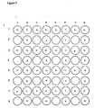
- Figure 3 is a plan view of an arrangement of unit capacitances for obtaining a capacity ratio of 32:16:8:4:2:1:1 in squares area of a 8 ⁇ 8 unit capacitances.
- a capacity of an unit capacitance is Cu
- a capacity of a capacitance with the maximum capacity is defined as 32Cu
- the capacitances following to the maximum are defined as 16Cu, 8Cu, 4Cu, 2Cu and Cu.
- a capacity is defined as a reference capacity of Cu.
- Figure 3 shows an arrangement of unit capacitances with coordinates 'i' of the horizontal direction and 'j' of the vertical direction 'j'.
- G ⁇ xij ⁇
- i odd, odd ⁇ .
- a sum of subsets g1 and g4 is defined as g5
- a sum of subsets g2 and g3 is defined as g6.
- the subset g5 or g6 is designated as unit capacitances for the capacitance component of most significant bit (MSB).
- MSB most significant bit
- Figure 4 shows an arrangement of g5, and unit capacitances of MSB are designated by a reference 'a'. This arrangement can be called 'zigzag arrangement'.
- step 2 unit capacitances for the second bit from MSB is selected. Since g5 is selected in step 1, unit capacitances included in g6 are selected in step 2. The subset g2 or g3 is selected. Figure 4 shows a condition that g2 is selected and the selected unit capacitance is shown by a reference 'b'. If g6 were selected, gl or g4 would be selected.
- step 3 unit capacitances are shown without references which are not selected in the step 2, as shown in Figure 4. Then, new coordinates of arrangement is given to the non-selected, and processes are repeated like step 1.
- Figure 5 shows new coordinates "i" (horizontal direction) and "j" (vertical direction) for non-selected 16 unit capacitances, and subset mentioned above is defined (selected unit capacitance is shown by x.).
- g5 or g6 is selected to be the third bit from MSB, which is the most significant bit among the bits undefined.
- Figure 6 shows an arrangement when g5 is selected, unit capacitances for the third bit is shown by 'a'. In Figure 6, selected unit capacitances are shown by ⁇ .
- g2 is selected to be the the forth bit.
- Figure 6 four unit capacitances for the forth bit is shown by a refernce 'b'.
- Non-selected unit capacitances exist as unit capacitances for a reference capacitance, then the total assignments are completed.
- unit capacitances for each capacitance are equally dispersed. Deviation of capacities due to positioning partiality is solved and high relative accuracy is obtained.
- the subset g5 or g6 is selected to be unit capacitances of MSB.
- step 1 When g5 is selected in step 1, then g2 or g3 is selected to be unit capacitances for the highest bit among bits after the selection of unit capacitances for MSB. When g6 is selected, gl or g4 is selected.
Landscapes
- Semiconductor Integrated Circuits (AREA)
Claims (1)
- Kapazitätserzeugungsverfahren zum Formen von Kapazitäts-Komponenten, welche Gewichte von Bits einer Binärzahl in einer hochintegrierten Schaltung (LSI) darstellen, mit den Schritten:gekennzeichnet durch die folgenden Schritte:Definieren einer Einheitskapazität mit einer vorgegebenen Form;Definieren eines Rechtecks aus einer Vielzahl der Einheitskapazitäten mit einer zum Erreichen der Ausbildung der gewünschten Gesamtkapazität notwendigen Zahl in einer zweidimensionalen Fläche der hochintegrierten Schaltung;SCHRITT 1: Definieren von Koordinaten (i,j) längs beider Seiten des Rechtecks einer Gruppe der gesamten Einheitskapazitäten als G = {xii}, Teilsätzen von g1 = {xij | i : gerade,j : gerade}, g2 = {xij | i : gerade, j : ungerade}, g3 = {xij | i: ungerade, j : gerade} und g4 = {xij | i : ungerade, jj: ungerade} und Definieren von Gruppen g5 = g1 ∪ g4 und g6 = g2 ∪ 93;SCHRITT 2: Wählen von g5 oder g6 als eine Gruppe von Einheitskapazitäten für eine Kapazitätskomponente, Darstellen des höchswertigsten Bits unter den Bits, für welche die Einheitskapazitäten noch nicht zugeordnet wurden;SCHRITT 3: wenn g5 gewählt ist, Auswählen von g2 oder g3 für das nächst-höchstwertigste Bit in dieser Stufe, sonst Auswählen von g1 oder g4 für das nächst-höchstwertigste Bit in dieser Stufe; undSCHRITT 4: wenn alle anderen Bits außer dem niederwertigsten Bit der Binärzahl bereits durch die Einheitskapazitäten definiert sind, Zuordnen der einen Hälfte des Restes der noch nicht zugeordneten Einheitskapazitäten zu dem niederwertigsten Bit und der anderen zu einem Referenzkondensator, und sonst Definieren neuer Koordinaten (i,j) für den Rest der Einheitskapazitäten, und Zurückkehren zu SCHRITT 1.
Applications Claiming Priority (6)
| Application Number | Priority Date | Filing Date | Title |
|---|---|---|---|
| JP261623/94 | 1994-09-30 | ||
| JP26162394A JP3353261B2 (ja) | 1994-09-30 | 1994-09-30 | キャパシタンス形成方法 |
| JP26161794A JPH08102521A (ja) | 1994-09-30 | 1994-09-30 | キャパシタンス形成方法 |
| JP261617/94 | 1994-09-30 | ||
| JP27168794A JP3353262B2 (ja) | 1994-10-11 | 1994-10-11 | キャパシタンス形成方法 |
| JP271687/94 | 1994-10-11 |
Publications (2)
| Publication Number | Publication Date |
|---|---|
| EP0704904A1 EP0704904A1 (de) | 1996-04-03 |
| EP0704904B1 true EP0704904B1 (de) | 1999-05-26 |
Family
ID=27335052
Family Applications (1)
| Application Number | Title | Priority Date | Filing Date |
|---|---|---|---|
| EP95115448A Expired - Lifetime EP0704904B1 (de) | 1994-09-30 | 1995-09-29 | Kapazitätserzeugungsverfahren |
Country Status (3)
| Country | Link |
|---|---|
| US (1) | US5734583A (de) |
| EP (1) | EP0704904B1 (de) |
| DE (1) | DE69509851T2 (de) |
Families Citing this family (10)
| Publication number | Priority date | Publication date | Assignee | Title |
|---|---|---|---|---|
| JPH09331024A (ja) * | 1996-06-07 | 1997-12-22 | Yozan:Kk | キャパシタンス構成方法 |
| JPH10142299A (ja) * | 1996-11-06 | 1998-05-29 | Yozan:Kk | 半導体集積回路装置内の素子特性測定回路 |
| US5973633A (en) * | 1996-12-20 | 1999-10-26 | Texas Instruments Incorporated | Weighted capacitor array with selective grouping to form array elements |
| US6330704B1 (en) | 1999-02-09 | 2001-12-11 | Coyote Systems, Inc. | Method and apparatus for three dimensional interconnect analysis |
| US6383858B1 (en) * | 2000-02-16 | 2002-05-07 | Agere Systems Guardian Corp. | Interdigitated capacitor structure for use in an integrated circuit |
| US6480137B2 (en) * | 2001-02-28 | 2002-11-12 | Texas Instruments Incorporated | Method of generating matched capacitor arrays |
| US6694493B2 (en) * | 2001-11-14 | 2004-02-17 | Sun Microsystems, Inc. | Decoupling capacitance assignment technique with minimum leakage power |
| KR100902503B1 (ko) * | 2002-08-12 | 2009-06-15 | 삼성전자주식회사 | 다층 수직 구조를 갖는 고용량 커패시터 |
| US20060236343A1 (en) * | 2005-04-14 | 2006-10-19 | Sbc Knowledge Ventures, Lp | System and method of locating and providing video content via an IPTV network |
| EP1863090A1 (de) * | 2006-06-01 | 2007-12-05 | Semiconductor Energy Laboratory Co., Ltd. | Halbleiterbauelement und Verfahren zur Herstellung eines Halbleiterbauelements |
Family Cites Families (10)
| Publication number | Priority date | Publication date | Assignee | Title |
|---|---|---|---|---|
| JPS58103163A (ja) * | 1981-12-16 | 1983-06-20 | Hitachi Ltd | 容量素子 |
| US4694403A (en) * | 1983-08-25 | 1987-09-15 | Nec Corporation | Equalized capacitance wiring method for LSI circuits |
| NL8403932A (nl) * | 1984-12-24 | 1986-07-16 | Philips Nv | Geintegreerde schakeling met kapaciteiten van verschillende kapaciteitswaarden. |
| JP2746762B2 (ja) * | 1990-02-01 | 1998-05-06 | 松下電子工業株式会社 | 半導体集積回路のレイアウト方法 |
| US5313090A (en) * | 1990-06-29 | 1994-05-17 | Nec Corporation | Bipolar memory cell having capacitors |
| US5245543A (en) * | 1990-12-21 | 1993-09-14 | Texas Instruments Incorporated | Method and apparatus for integrated circuit design |
| US5278105A (en) * | 1992-08-19 | 1994-01-11 | Intel Corporation | Semiconductor device with dummy features in active layers |
| US5471090A (en) * | 1993-03-08 | 1995-11-28 | International Business Machines Corporation | Electronic structures having a joining geometry providing reduced capacitive loading |
| JPH06326106A (ja) * | 1993-03-18 | 1994-11-25 | Sony Corp | ダミーパターンの形成方法 |
| JPH07121860A (ja) * | 1993-10-29 | 1995-05-12 | Victor Co Of Japan Ltd | 磁気記録媒体 |
-
1995
- 1995-09-29 DE DE69509851T patent/DE69509851T2/de not_active Expired - Fee Related
- 1995-09-29 EP EP95115448A patent/EP0704904B1/de not_active Expired - Lifetime
- 1995-09-29 US US08/536,326 patent/US5734583A/en not_active Expired - Fee Related
Also Published As
| Publication number | Publication date |
|---|---|
| DE69509851T2 (de) | 1999-09-30 |
| EP0704904A1 (de) | 1996-04-03 |
| US5734583A (en) | 1998-03-31 |
| DE69509851D1 (de) | 1999-07-01 |
Similar Documents
| Publication | Publication Date | Title |
|---|---|---|
| EP0704904B1 (de) | Kapazitätserzeugungsverfahren | |
| US7595229B2 (en) | Configurable integrated circuit capacitor array using via mask layers | |
| EP0248513B1 (de) | Verfahren zur Routen-Festlegung | |
| DE69933712T2 (de) | Stromzellenanordnung | |
| US5966047A (en) | Programmable analog array and method | |
| US6157214A (en) | Wiring of cells in logic arrays | |
| US4858143A (en) | Work ordering routine for use in a method of routing | |
| JPH0786407A (ja) | 集積回路の多層配線方法 | |
| Sayed et al. | Automatic generation of common-centroid capacitor arrays with arbitrary capacitor ratio | |
| EP1191698A2 (de) | D/A-Wandler des Kapazitätsnetzwerkstyps mit Thermometerdekodierer und Kapazitätsnetzwerk | |
| DE3587055T2 (de) | Verfahren zur verteilung der leitungsbelastung auf einer schaltkarte oder auf einem verbindungspackage mit jeweils mehreren verdrahtungsebenen. | |
| US6215786B1 (en) | Implementation of multi-stage switching networks | |
| DE60128426T2 (de) | Zellenanordnung von Stromquellen, Verfahren zur Auswahl von Stromquellen und Digital-Analog-Wandler des Stromadditionstyps | |
| US6982454B2 (en) | Metal-metal capacitor array | |
| US7612984B2 (en) | Layout for capacitor pair with high capacitance matching | |
| JPS61292341A (ja) | 半導体集積回路 | |
| CN111129304A (zh) | Mom电容器、电容阵列结构以及其制造方法 | |
| JPS5866343A (ja) | 半導体集積回路装置 | |
| EP0135019B1 (de) | Verbindung von Elementen auf ein Substrat mit integrierter Schaltung | |
| US7428719B2 (en) | Layout of network using parallel and series elements | |
| JP3353262B2 (ja) | キャパシタンス形成方法 | |
| JPH0214789B2 (de) | ||
| JPH07211860A (ja) | キャパシタンス形成方法 | |
| US7126206B2 (en) | Distributed capacitor array | |
| JP3353261B2 (ja) | キャパシタンス形成方法 |
Legal Events
| Date | Code | Title | Description |
|---|---|---|---|
| PUAI | Public reference made under article 153(3) epc to a published international application that has entered the european phase |
Free format text: ORIGINAL CODE: 0009012 |
|
| AK | Designated contracting states |
Kind code of ref document: A1 Designated state(s): DE FR GB |
|
| 17P | Request for examination filed |
Effective date: 19960904 |
|
| 17Q | First examination report despatched |
Effective date: 19970321 |
|
| GRAG | Despatch of communication of intention to grant |
Free format text: ORIGINAL CODE: EPIDOS AGRA |
|
| GRAG | Despatch of communication of intention to grant |
Free format text: ORIGINAL CODE: EPIDOS AGRA |
|
| GRAH | Despatch of communication of intention to grant a patent |
Free format text: ORIGINAL CODE: EPIDOS IGRA |
|
| GRAH | Despatch of communication of intention to grant a patent |
Free format text: ORIGINAL CODE: EPIDOS IGRA |
|
| GRAA | (expected) grant |
Free format text: ORIGINAL CODE: 0009210 |
|
| AK | Designated contracting states |
Kind code of ref document: B1 Designated state(s): DE FR GB |
|
| REF | Corresponds to: |
Ref document number: 69509851 Country of ref document: DE Date of ref document: 19990701 |
|
| ET | Fr: translation filed | ||
| PLBE | No opposition filed within time limit |
Free format text: ORIGINAL CODE: 0009261 |
|
| STAA | Information on the status of an ep patent application or granted ep patent |
Free format text: STATUS: NO OPPOSITION FILED WITHIN TIME LIMIT |
|
| 26N | No opposition filed | ||
| PGFP | Annual fee paid to national office [announced via postgrant information from national office to epo] |
Ref country code: GB Payment date: 20010917 Year of fee payment: 7 |
|
| PGFP | Annual fee paid to national office [announced via postgrant information from national office to epo] |
Ref country code: FR Payment date: 20010921 Year of fee payment: 7 |
|
| PGFP | Annual fee paid to national office [announced via postgrant information from national office to epo] |
Ref country code: DE Payment date: 20011026 Year of fee payment: 7 |
|
| REG | Reference to a national code |
Ref country code: GB Ref legal event code: IF02 |
|
| PG25 | Lapsed in a contracting state [announced via postgrant information from national office to epo] |
Ref country code: GB Free format text: LAPSE BECAUSE OF NON-PAYMENT OF DUE FEES Effective date: 20020929 |
|
| PG25 | Lapsed in a contracting state [announced via postgrant information from national office to epo] |
Ref country code: DE Free format text: LAPSE BECAUSE OF NON-PAYMENT OF DUE FEES Effective date: 20030401 |
|
| GBPC | Gb: european patent ceased through non-payment of renewal fee |
Effective date: 20020929 |
|
| PG25 | Lapsed in a contracting state [announced via postgrant information from national office to epo] |
Ref country code: FR Free format text: LAPSE BECAUSE OF NON-PAYMENT OF DUE FEES Effective date: 20030603 |
|
| REG | Reference to a national code |
Ref country code: FR Ref legal event code: ST |