EP0704910B1 - Transistor à couche mince et son procédé de fabrication - Google Patents
Transistor à couche mince et son procédé de fabrication Download PDFInfo
- Publication number
- EP0704910B1 EP0704910B1 EP95306522A EP95306522A EP0704910B1 EP 0704910 B1 EP0704910 B1 EP 0704910B1 EP 95306522 A EP95306522 A EP 95306522A EP 95306522 A EP95306522 A EP 95306522A EP 0704910 B1 EP0704910 B1 EP 0704910B1
- Authority
- EP
- European Patent Office
- Prior art keywords
- gate electrode
- channel
- recess
- forming
- layer
- Prior art date
- Legal status (The legal status is an assumption and is not a legal conclusion. Google has not performed a legal analysis and makes no representation as to the accuracy of the status listed.)
- Expired - Lifetime
Links
Images

Classifications
-
- H—ELECTRICITY
- H10—SEMICONDUCTOR DEVICES; ELECTRIC SOLID-STATE DEVICES NOT OTHERWISE PROVIDED FOR
- H10D—INORGANIC ELECTRIC SEMICONDUCTOR DEVICES
- H10D30/00—Field-effect transistors [FET]
- H10D30/01—Manufacture or treatment
- H10D30/021—Manufacture or treatment of FETs having insulated gates [IGFET]
- H10D30/031—Manufacture or treatment of FETs having insulated gates [IGFET] of thin-film transistors [TFT]
- H10D30/0321—Manufacture or treatment of FETs having insulated gates [IGFET] of thin-film transistors [TFT] comprising silicon, e.g. amorphous silicon or polysilicon
-
- H—ELECTRICITY
- H10—SEMICONDUCTOR DEVICES; ELECTRIC SOLID-STATE DEVICES NOT OTHERWISE PROVIDED FOR
- H10D—INORGANIC ELECTRIC SEMICONDUCTOR DEVICES
- H10D30/00—Field-effect transistors [FET]
- H10D30/01—Manufacture or treatment
- H10D30/021—Manufacture or treatment of FETs having insulated gates [IGFET]
- H10D30/031—Manufacture or treatment of FETs having insulated gates [IGFET] of thin-film transistors [TFT]
- H10D30/0312—Manufacture or treatment of FETs having insulated gates [IGFET] of thin-film transistors [TFT] characterised by the gate electrodes
- H10D30/0314—Manufacture or treatment of FETs having insulated gates [IGFET] of thin-film transistors [TFT] characterised by the gate electrodes of lateral top-gate TFTs comprising only a single gate
-
- H—ELECTRICITY
- H10—SEMICONDUCTOR DEVICES; ELECTRIC SOLID-STATE DEVICES NOT OTHERWISE PROVIDED FOR
- H10D—INORGANIC ELECTRIC SEMICONDUCTOR DEVICES
- H10D30/00—Field-effect transistors [FET]
- H10D30/60—Insulated-gate field-effect transistors [IGFET]
- H10D30/67—Thin-film transistors [TFT]
- H10D30/6704—Thin-film transistors [TFT] having supplementary regions or layers in the thin films or in the insulated bulk substrates for controlling properties of the device
- H10D30/6713—Thin-film transistors [TFT] having supplementary regions or layers in the thin films or in the insulated bulk substrates for controlling properties of the device characterised by the properties of the source or drain regions, e.g. compositions or sectional shapes
- H10D30/6715—Thin-film transistors [TFT] having supplementary regions or layers in the thin films or in the insulated bulk substrates for controlling properties of the device characterised by the properties of the source or drain regions, e.g. compositions or sectional shapes characterised by the doping profiles, e.g. having lightly-doped source or drain extensions
-
- H—ELECTRICITY
- H10—SEMICONDUCTOR DEVICES; ELECTRIC SOLID-STATE DEVICES NOT OTHERWISE PROVIDED FOR
- H10D—INORGANIC ELECTRIC SEMICONDUCTOR DEVICES
- H10D30/00—Field-effect transistors [FET]
- H10D30/60—Insulated-gate field-effect transistors [IGFET]
- H10D30/67—Thin-film transistors [TFT]
- H10D30/6729—Thin-film transistors [TFT] characterised by the electrodes
- H10D30/673—Thin-film transistors [TFT] characterised by the electrodes characterised by the shapes, relative sizes or dispositions of the gate electrodes
-
- H—ELECTRICITY
- H10—SEMICONDUCTOR DEVICES; ELECTRIC SOLID-STATE DEVICES NOT OTHERWISE PROVIDED FOR
- H10D—INORGANIC ELECTRIC SEMICONDUCTOR DEVICES
- H10D30/00—Field-effect transistors [FET]
- H10D30/60—Insulated-gate field-effect transistors [IGFET]
- H10D30/67—Thin-film transistors [TFT]
- H10D30/674—Thin-film transistors [TFT] characterised by the active materials
-
- H—ELECTRICITY
- H10—SEMICONDUCTOR DEVICES; ELECTRIC SOLID-STATE DEVICES NOT OTHERWISE PROVIDED FOR
- H10D—INORGANIC ELECTRIC SEMICONDUCTOR DEVICES
- H10D30/00—Field-effect transistors [FET]
- H10D30/60—Insulated-gate field-effect transistors [IGFET]
- H10D30/67—Thin-film transistors [TFT]
- H10D30/6757—Thin-film transistors [TFT] characterised by the structure of the channel, e.g. transverse or longitudinal shape or doping profile
Definitions
- the present invention relates generally to semiconductor devices and more specifically to a transistor formed from a film of semiconductor material on a dielectric substrate for use in an SRAM memory cell.
- TFTs Thin-film transistors
- SRAM static random access memory
- a P-channel polysilicon transistor in a six transistor SRAM cell is well known in the prior art, see U.S. Patent No. 5,135,888; 5,187,114; and 5,204,279; each of which are incorporated herein by reference.
- a TFT is a field-effect transistor (FET) having its channel, drain, and source regions formed from a strip of semiconductor material, such as polysilicon, that has been formed on a dielectric substrate, such as SiO 2 , quartz or glass.
- FET field-effect transistor
- a TFT may be formed in a stacked arrangement, above a semiconductor structure, such as the other transistors in an SRAM cell.
- Such stacking of integrated-circuit components often provides a significant reduction in the area of the integrated circuit.
- Murakami et al. teach a stacked transistor SRAM cell in their article titled "A 21 mW CMOS SRAM for Battery Operation," ISSCC, pg. 46 (1991) presented on behalf of Mitsubishi Electric.
- a TFT is often larger than its single-crystal counterparts, i.e., transistors in a single-crystal semiconductor subsrate. Additionally, the switching speed of a TFT is often too slow for certain applications.
- European patent application EP-A-0401577 discloses a semiconductor transistor having a semiconductor-on-insulator structure and comprising a layer of semiconductor on an insulator substrate, source and drain regions formed in the semiconductor layer, a channel region also formed in the semiconductor layer between the source and drain regions, and a gate electrode in correspondence to the channel region and insulated from the channel region by a gate insulator film.
- French Patent Application FR-A-2698210 corresponding to the preamble of claim 1 discloses a Thin Film Transistor (TFT) structure having an insulator substrate with a recess formed therein and the channel region of the TFT formed within the recess.
- TFT Thin Film Transistor
- EP-A-0578926 discloses a Thin Film Transistor formed by forming an opening in a dielectric layer overlying a substrate and forming a semiconductor sidewall spacer around the perimeter of the opening, the sidewall spacer acting as the channel region of the transistor.
- a control electrode is formed substantially in the opening, insulated from the sidewall spacer by a dielectric layer.
- a semiconductor structure comprising a dielectric substrate having a surface and having a recess formed therein, characterised in that a layer of semiconductor material is positioned on said surface and in said recess and has within said recess a channel region, said layer of semiconductor material also having source and drain, regions; a gate electrode formed overlying said surface and having an end portion extending over only a portion of said recess to overlap said channel region; and an insulator positioned between said channel region and said end portion of said gate electrode.
- a method for forming a transistor comprising forming a recess in a dielectric substrate such that said recess and a surface of said substrate are contiguous, characterised by forming a gate electrode on said surface of said dielectric substrate, said gate electrode having an end portion that extends over only a portion of said recess; forming an insulator on exposed portions of said gate electrode; forming a layer of semiconductor material on said surface and in said recess such that said gate electrode overlays said semiconductor layer; forming a channel region in said semiconductor material within said recess; and forming drain and source regions in said semiconductor material adjacent opposing ends of said channel to provide a transistor.
- a transistor is formed on a dielectric layer.
- the dielectric layer is preferably an oxide layer overlaying integrated circuit elements in a silicon substrate.
- the channel region is within a recess of the substrate, below the surface.
- a gate electrode is in substantial alignment with the channel. Because the gate electrode and the channel are self-aligned, the channel length can be precisely formed and is less than gate electrode width and twice the insulator thickness.
- the source region includes lightly doped source and drain regions that are adjacent to the channels that are automatically formed without additional process steps and with one less step that is normally required in the prior art.
- One advantage of the invention is that the transistor is smaller than existing TFTs.
- Another advantage is that it is easier to manufacture than existing TFTs.
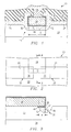
- Figure 1 is a cut-away end view of a semiconductor structure formed according to the present invention.
- Figure 2 is a top view of a portion of the structure of Figure 1.
- Figure 3 is a cut-away side view of the structure of Figure 2 taken along lines A-A of Figure 2.
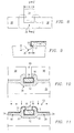
- Figure 4 is a top view of a semiconductor structure that has been etched.
- Figure 5 is a cut-away end view of the structure of Figure 4 taken along lines B-B of Figure 4.
- Figure 6 is the structure of Figure 5 after a dielectric and a semiconductor layer have been formed.
- Figure 7 is a view of the structure of Figure 6 taken along lines positioned at C-C of Figure 4.
- Figure 8 is a top view of the structure of Figure 7 with a mask layer in place and after an etch step.
- Figure 9 is a partial cross-sectional view of Figure 8, taken along lines C-C.
- Figure 10 is an end view of the structure of Figure 9 taken along lines C-C of Figure 4.
- Figure 11 is a view of the structure of Figure 10 after the removal of the mask layer and the addition of a dielectric layer.
- FIG. 1 is a cut-away cross-sectional view of a semiconductor structure 10, which in the illustrated embodiment includes a thin-film transistor (TFT) 11.
- TFT 11 has a channel region 12 that has a length L and is self-aligned with the gate electrode 14. That is, channel region 12 has substantially the same length as the width w of gate electrode 14.
- Such self-alignment both reduces the size of TFT 11 over existing TFTs, and reduces parasitic capacitances, such as the Miller capacitance, that may be caused by gate electrode 14 extensively overlapping the source and drain regions 18 and 20, as may occur in existing devices.
- parasitic capacitances such as the Miller capacitance
- TFT 11 is formed on a substrate 22, which is typically formed from a dielectric material, such as SiO 2 , a glass layer, or quartz.
- a layer 24 of semiconductor material, typically polysilicon is formed over substrate 22 and includes channel region 12 and drain and source regions 18 and 20.
- An insulating dielectric layer 26 may be formed above the polysilicon layer 24 to insulate polysilicon layer 24 from later layers, such as a gate-electrode contact 28.
- source region 18 may include a lightly doped source region 30 and drain region 20 may include a lightly doped drain region 32.
- semiconductor structure 10, which includes TFT 11 and substrate 22, may be formed over a SRAM cell 34.
- the TFT 11 is the P-channel device for a six transistor SRAM cell.
- the area of the SRAM cell may be greatly reduced over existing cells that use P-channel transistor devices that are formed on the same horizontal plane as the SRAM cell.
- This P-channel transistor may directly replace the P-channel transistors of current six-T SRAM design, such as those previously cited herein and provide an overall smaller area memory cell size than these prior art devices.
- Figure 2 is a top view of the semiconductor structure 10 of Figure 1. For clarity, contact 28 and insulating layer 26 are omitted from Figure 2. This shows the polysilicon layer 24 having the source/drain 18 and 20 and the channel 12 formed therein. The gate 14 overlays the channel region 12.
- Figure 3 shows a cut-away side view of semiconductor structure 10 taken along lines A-A of Figure 2. Again for clarity, insulator 26 and contact 28 are omitted from Figure 3.
- channel region 12 is formed in a portion of recess 36 in substrate 22.
- An oxide layer 38 is formed between channel 12 and the gate electrode 14.
- a portion 39 of the recess 36 does not have a channel region therein.
- a portion 41 of gate electrode 14 extends beyond an edge 41 over the recess 36 to overlay and be contiguous with channel region 12.
- This portion 39 is filled with the same polysilicon layer 24 in one embodiment, but because of its spacing from the gate electrode 14, it does not effectively function as a part of channel region 12.
- the portion 39 may be void or filled with an insulating structure such as SiO 2 or the like.
- FIGS 4-11 together illustrate a method for forming semiconductor 10, which includes TFT 11 formed on substrate 22.
- SRAM 34 is not shown, it being understood that structure 10 may be formed over SRAM 34 or may be formed independently thereof, the design rules and SRAM cell layout being design choices by those of skill in the art of the many possible choices.
- gate electrode 14 is formed thereon.
- a film of polysilicon having a thickness of approximately 0.5 ⁇ m is deposited upon substrate 22 by a low-pressure chemical vapor deposition (LPCVD).
- LPCVD low-pressure chemical vapor deposition
- the polysilicon film is then doped according to existing methods to become more conductive.
- the polysilicon film may be doped N+.
- width W is approximately 4 ⁇ , where ⁇ is the minimum process dimension.
- a mask layer 60 which in one embodiment of the invention is a layer of photoresist film, is deposited over strips 14.
- An opening 62 is formed in layer 60 such that it provides an opening over an end portion of the strip 14.
- the exposed regions of substrate 22 are isotropically etched to give an undercut region as shown by dotted line 64.
- this isotropic etch is performed using an aqueous solution of dilute hydrogen fluoride (HF), such as buffered oxide etch (BOE), and is continued until the exposed regions of substrate 22 are etched to a desired depth r.
- Figure 5 shows a view of the structure of Figure 4 taken along lines B-B.
- the structure includes photoresist 60, strip 14, and recess 36, which has been formed by the isotropic etch described above in conjunction with Figure 4. The etch produces an undercut of distance d under the gate electrode 14.
- gate insulator 16 is formed by any acceptable technique.
- gate insulator 16 is an oxide that is grown in dry O 2 over the exposed surface portions of strip 14, or other thermal oxidation techniques, as are known.
- Gate oxide 16 may have a thickness in a range of approximately 100-500 ⁇ .
- the oxide 16 is formed on all exposed portions of the gate electrode in a single step.
- the oxide layer on the top of the gate electrode 14, on the sidewalls, and on the bottom, are all formed simultaneously.
- a process advantage is obtained by forming a gate sidewall oxide in the same step as the top oxide layer and the lower gate oxide on the bottom side of the gate electrode.
- a semiconductor film 66 is formed on insulator 16 and on the exposed surface regions of substrate 22, including those within recess 36.
- semiconductor film 66 is formed from a layer of amorphous silicon that is deposited over substrate 22 and insulator 16 to a thickness of approximately 7,000 ⁇ .
- the layer 66 is polysilicon of a suitable thickness.
- a variety of techniques for forming amorphous silicon and polysilicon are known in the art and any suitable techniques may be used as selected by the process designs as being compatible with the process.
- Figure 7 is a view of the structure of Figure 6 taken along lines C-C of Figure 4. As shown, the gate electrode 14 extends over the recess 36 to overlay a portion of film 66 that is within recess 36. This will later form the channel region 12 of the transistor.
- a second mask layer 68 is formed over film 66 to permit etching of strip 24 using standard, existing photolithographic process.
- the photoresist 68 is partially removed to create an aperture 69 and leave a layer 68 on top of the portions of the semiconductor layer 66 that will become the source and drain region of the semiconductor strip 24.
- the exposed portions of semiconductor film 66 are anisotropically etched to form channel region 12 in recess 36 as shown in Figure 9.
- the exposed portions of film 66 are etched using an ion-assisted plasma etching process.
- channel 12 should be made to provide a sufficiently high resistance when TFT 11 is in an off state, i.e., when channel region 12 is in a nonconductive state.
- the off-resistance is extremely high, at or above the teraohm 50 range, that from a practical circuit view it approaches infinity and the on-resistance is quite high, usually in the mega-ohm or higher range.
- a P-channel transistor it does switch on, but is not designed to be a high current carrying member when on; rather, it is designed to be conductive but to have a very low current, because of a very high channel resistivity when on.
- Figure 9 shows the device partially formed with the channel region 12 having a dimension d corresponding to the undercut depth d and a total maximum height equal to the depth r of recess 36.
- the channel region 12 is thus a narrow strip having a length L approximately equal to width of the gate electrode 14, a depth that can be, at maximum, the depth of the recess 36, and thickness that is, at maximum, the undercut distance d.
- the distance d and recess depth r may be less than the minimum feature size ⁇ because they are formed from etch steps and undercut etches, not by standard photolithographic techniques.
- the channel 12 can thus be very small in these critical dimensions, as compared to prior art devices, and yet the forming steps insure that the channel 12 itself will not be overetched or discontinuities occur because the poly layer 14 protects the channel 12 from an anisotropic etch. Overetching of the film 24 will not risk harming the channel 12 because it is under the overhang 41 of the gate electrode 14. This can produce significant advantages in the process control steps not possible with prior art polysilicon film transistors, particularly if the end use is for an SRAM.
- Figure 10 is as view of the structure of Figure 8 taken along line C-C of Figure 4 after the above-described anisotropic etching process.
- channel region 12 After channel region 12 has been formed, it is ion-implanted to adjust the threshold voltage and form the desired type of device, i.e., either P-channel or N-channel.
- a P-channel device is formed by phosphorous-ion implanting channel 12 in a range of approximately 10 12 atoms/cm 2 .
- the energy of this ion implant is selected such that it can penetrate the overlying strip 14.
- An adequate implant energy for this is approximately 300 KeV.
- a rotating wafer technique or another equivalent technique that will provide access to the exposed boundary or edge 37 ( Figure 3) of channel region 12.
- Figure 3 By having the same mask in place for both the etch of the channel region 12 and the implant of the channel, self-alignment of the channel is obtained.
- photoresist layer 68 is removed according to existing techniques and if the layer 66 is amorphous silicon, it is crystallized, i.e., converted into polysilicon strip 24 ( Figure 1).
- layer 66 is exposed to a long, low temperature anneal in N 2 or Ar in order to convert the amorphous silicon into strip 24 of large grained polysilicon.
- Such an anneal is typically performed within a temperature of approximately 475-600°C for a time period in a range of approximately 20-100 hours.
- the anneal temperature should be low enough so that additional nucleation sites or small crystals are not generated in the amorphous silicon, but high enough so that existing crystallites may grow through solid state diffusion to produce grain sizes of approximately 5 ⁇ m and larger.
- layer 66 may be converted into strip 24 of large grain polysilicon using existing laser techniques. It is known that larger crystal grains within polysilicon layer 24 often produce improved TFTs, because larger grains reduce the number of charges that may be stored at carrier traps, which are primarily located at the grain boundaries.
- the layer 24 can be formed initially of acceptable polysilicon and the process continue without need for a long-term anneal.
- an oxide 72 is formed over the exposed portions of strip 24.
- the Figure 11 structure is lightly oxidized in steam at a temperature of approximately 850°C to grow a layer 72 of silicon dioxide that is approximately 200 ⁇ thick.
- structure 10 is blanket ion implanted to form drain and source regions 20 and 18.
- structure 10 is ion implanted with boron using a dose of approximately 10 15 atoms/cm 2 at an energy of approximately 150 KeV or possibly an even higher dose.
- Such an implant is made in an substantially perpendicular direction to the surface of structure 10, as shown by the multiple arrows in Figure 11.
- such an implant provides a sufficient heavy dopant concentration for good conductivity in the portions of source 18 and drain 20 outside lightly doped regions 30 and 32 an impurity concentration of approximately 10 19 atoms/cm 3 .
- LDD regions 30 and 32 Immediately after the implant process, very little boron is present in LDD regions 30 and 32. This is because it has a larger volume and also because it is protected in part from the thickness of the poly two layer, the poly one layer and the sidewalls of the gate oxide 16. Structure 10 is then submitted to a heat treatment of approximately 1 hr in a temperature range between 900-925°C to drive a light concentration of the implanted boron into regions 30 and 32 such that near the boundaries with channel region 12 (which in this aspect of the invention is doped N-) the impurity concentration is in the range to 10 17 -10 18 atoms/cm 3 or even less in some embodiments. Such a heat treatment forms LDD regions 30 and 32 of the P- type. Alternatively, RTA methods may be used for the boron drive-in step.
- the lightly doped source and drain regions are advantageously created without an additional ion implant step. This is possible because, among other things, the layer 24 is thicker at the source/drain regions immediately adjacent the channel and also because the source/drain regions are much deeper adjacent the channel, the channel 12 being in a recess below the surface. Thus, for the same implant dose, the ions are spread over a larger volume when diffused and the final impurity concentration is less. Further, for an ion dose at the surface, the ions diffuse downward.
- the deeper regions of the poly layer 24 can have a lower final concentration of dopants by selective control of the thermal steps occurring after the ion implant, taking into account the impurities' diffusion characteristics.
- the source/drain and LDD structure are automatically self-aligned to the channel 12 because the poly one layer 14 and gate oxide 16 having sidewalls surrounding this layer will act as a self-aligning edge stop to the ion implant that, when diffused, creates the LDD structure.
- the oxide sidewalls provide a stop for the vertical ion dose implant, being a good mask edge and the gate oxide prevents later diffusions from placing excessive counter dopants in respective polysilicon layers.
- the self-alignment of the LDD structure is also attainable by use of either of these techniques alone, or in combination.
- TFT 11 may be hydrogen passivated to reduce the trap density at the grain boundaries within layer 24. Such a reduction often reduces the threshold voltage and subthreshold leakage currents.
- This hydrogen passivation may be performed using a long bake in forming gas or hydrogen (H), applying plasma etch chemical vapor deposition (PECVD) silicon nitrite layers, immersing structure 10 in a hydrogen plasma at a temperature of approximately 300°C, or by high dose ion implantation with protons.
- H forming gas or hydrogen
- PECVD plasma etch chemical vapor deposition
- TFT 11 may now be completed and integrated with other devices by adding appropriate insulating layers, contacts, vias and metal films, as is known in the art, a final product being shown in Figure 1.
- TFT 11 is not limited except as by the appended claims.
- a method for forming a P-channel TFT 11 is disclosed, one may form TFT 11 as an N-channel without departing from the spirit and scope of the invention.
- gate electrode 14 and film 66 have been described as poly one and poly two, this does not require a particular sequence of these two layers, unless the claims so specify.
- the layers may be poly two, three or four, the particular level of polysilicon not being critical to the invention.
- strip 14, which forms the gate electrode of TFT 11 may be formed from an electrically conductive material other than polysilicon.
Landscapes
- Thin Film Transistor (AREA)
- Semiconductor Memories (AREA)
Claims (14)
- Structure semiconductrice comprenant :un substrat diélectrique (22) comportant une surface et un évidement (36), caractérisé en ce que :une couche de matériau semiconducteur (24) est placée sur la surface et dans l'évidement (36) et comporte à l'intérieur de l'évidement une région de canal (12), la couche de matériau semiconducteur (24) comportant également des régions de source et de drain (18, 20) ;une électrode de grille (14) formée sur la surface a une partie d'extrémité (41) qui s'étend sur seulement une partie de l'évidement (36) pour recouvrir la région de canal (12) ; etune couche isolante (16) est placée entre la région de canal (12) et la partie d'extrémité (41) de l'électrode de grille (14).
- Structure selon la revendication 1, dans laquelle une partie de la région de source (18) et une partie de la région de drain (20) sont à l'intérieur de l'évidement (36) et des parties de chacune sont sur la surface du substrat diélectrique (22) à l'extérieur de l'évidement (36).
- Structure selon la revendication 1 ou 2, dans laquelle la région de source (18) inclut une région de source légèrement dopée (30) adjacente au canal (12) et une région de source complémentaire écartée du canal, et dans laquelle la région de drain comprend une région de drain légèrement dopée (32) adjacente au canal (12) et une région de drain complémentaire écartée du canal.
- Structure selon la revendication 3, dans laquelle au moins une partie de la région de source légèrement dopée (30) et une partie de la région de drain légèrement dopée (32) sont situées à l'intérieur de l'évidement (36).
- Structure selon la revendication 1 ou 2, dans laquelle l'électrode de grille (14) a deux parois latérales opposées recouvertes d'une couche d'oxyde, dans laquelle une partie de la région de source (18) est adjacente à une première des deux parois latérales et une partie de la région de drain (20) est adjacente à une seconde des deux parois latérales, et dans laquelle la couche isolante (16) sépare la région de source (18) de la première paroi latérale et sépare la région de drain (20) de la seconde paroi latérale.
- Structure selon la revendication 5, dans laquelle la région de source (18) comprend une région de source légèrement dopée (30) adjacente au canal (12) et à la première paroi latérale et une région de source complémentaire écartée du canal, et dans laquelle la région de drain (20) comprend une région de drain légèrement dopée (32) adjacente au canal (12) et à la seconde paroi latérale et une région de drain complémentaire écartée du canal.
- Structure selon l'une quelconque des revendications 3, 4 et 6, dans laquelle les régions de source et de drain légèrement dopées (30, 32) immédiatement adjacentes au canal (12) ont un plus grand volume que les régions de source et de drain complémentaires (18, 20) écartées du canal (12).
- Structure selon l'une quelconque des revendications précédentes, dans laquelle la couche de semiconducteur (24) recouvre une partie de l'électrode de grille (14), est adjacente à l'électrode de grille (14) et est recouverte par la partie d'extrémité (48) de l'électrode de grille (14).
- Structure selon l'une des revendications précédentes, dans laquelle la couche isolante (16) recouvre deux parties de parois latérales, une partie de la paroi supérieure et une partie de la paroi inférieure de l'électrode de grille (14).
- Procédé de fabrication d'un transistor, comprenant :la formation d'un évidement (36) dans un substrat diélectrique (22) de sorte que l'évidement (36) et une surface du substrat soient contigués, caractérisé en ce qu'il comprend les étapes suivantes :former une électrode de grille (14) sur ladite surface du substrat diélectrique (22), l'électrode de grille ayant une partie d'extrémité (41) qui s'étend sur seulement une partie de l'évidement (36) ;former un isolant (16) sur les parties exposées de l'électrode de grille (14) ;former une couche d'un matériau semiconducteur (24) sur la surface et dans l'évidement (36) de sorte que l'électrode de grille (14) recouvre la couche de matériau semiconducteur (24) ;former une région de canal (12) dans le matériau semiconducteur à l'intérieur de l'évidement (36) ; etformer des régions de drain et de source (18, 20) dans le matériau semiconducteur (24) adjacentes aux extrémités opposées du canal (12) pour produire un transistor.
- Procédé selon la revendication 10, dans lequel l'étape de formation de l'électrode de grille (14) comprend les étapes suivantes :déposer un film de silicium polycristallin sur la surface ;former une couche de masquage sur le film ;graver les parties exposées du film pour former l'électrode de grille (14) ; etenlever la couche de masquage.
- Procédé selon les revendications 10 ou 11, dans lequel l'étape de formation de l'évidement (36) comprend les étapes suivantes :former après que l'électrode de grille (14) a été formée, une couche de masquage (60) qui expose la partie d'extrémité (41) de l'électrode de grille (14) et une partie de la surface de substrat adjacente à la partie d'extrémité ; etgraver de façon isotrope la partie de substrat exposée de façon à sous-graver la partie d'extrémité (41) de l'électrode de grille (14).
- Procédé selon l'une quelconque des revendications 10 à 12, dans lequel les étapes de formation d'une couche de matériau semiconducteur et de formation d'une région de canal comprennent les étapes suivantes :déposer un film de silicium amorphe (66) sur la surface du substrat (22) et dans l'évidement (36) ;former une couche de masquage (68) sur le film de silicium amorphe ;graver de façon anisotrope le film de silicium amorphe pour laisser une bande à l'intérieur de l'évidement ;implanter un dopant dans une partie de la bande restante dans l'évidement pour former le canal (12) ;enlever la couche de masquage ; ettransformer la bande en silicium polycristallin (24).
- Procédé selon l'une quelconque des revendications 10 à 12, dans laquelle l'étape de formation de la couche de semiconducteur inclut l'étape suivante :
former une couche en silicium recouvrant l'électrode de grille et dans l'évidement recouverte par l'électrode de grille pour fournir une partie de la couche de semiconducteur sur l'électrode de grille, une partie sur le côté de l'électrode de grille et une partie sous l'électrode de grille.
Applications Claiming Priority (2)
| Application Number | Priority Date | Filing Date | Title |
|---|---|---|---|
| US08/316,633 US5557126A (en) | 1994-09-30 | 1994-09-30 | Thin-film transistor and method for forming the same |
| US316633 | 1994-09-30 |
Publications (3)
| Publication Number | Publication Date |
|---|---|
| EP0704910A2 EP0704910A2 (fr) | 1996-04-03 |
| EP0704910A3 EP0704910A3 (fr) | 1997-09-03 |
| EP0704910B1 true EP0704910B1 (fr) | 2001-11-28 |
Family
ID=23229927
Family Applications (1)
| Application Number | Title | Priority Date | Filing Date |
|---|---|---|---|
| EP95306522A Expired - Lifetime EP0704910B1 (fr) | 1994-09-30 | 1995-09-15 | Transistor à couche mince et son procédé de fabrication |
Country Status (4)
| Country | Link |
|---|---|
| US (1) | US5557126A (fr) |
| EP (1) | EP0704910B1 (fr) |
| JP (1) | JP4246801B2 (fr) |
| DE (1) | DE69524178T2 (fr) |
Families Citing this family (7)
| Publication number | Priority date | Publication date | Assignee | Title |
|---|---|---|---|---|
| JPH09275209A (ja) | 1996-04-04 | 1997-10-21 | Honda Motor Co Ltd | 高電子移動度トランジスタ及びその製造方法 |
| US6060749A (en) * | 1998-04-23 | 2000-05-09 | Texas Instruments - Acer Incorporated | Ultra-short channel elevated S/D MOSFETS formed on an ultra-thin SOI substrate |
| KR100324591B1 (ko) * | 1998-12-24 | 2002-04-17 | 박종섭 | 티타늄 알루미늄 질소 합금막을 상부전극의 확산방지막으로서 이용하는 캐패시터 제조 방법 |
| US6660598B2 (en) | 2002-02-26 | 2003-12-09 | International Business Machines Corporation | Method of forming a fully-depleted SOI ( silicon-on-insulator) MOSFET having a thinned channel region |
| US7306552B2 (en) * | 2004-12-03 | 2007-12-11 | Samsung Electronics Co., Ltd. | Semiconductor device having load resistor and method of fabricating the same |
| JP2007081335A (ja) * | 2005-09-16 | 2007-03-29 | Renesas Technology Corp | 半導体装置 |
| CN103730511B (zh) * | 2013-12-26 | 2016-03-23 | 京东方科技集团股份有限公司 | 薄膜晶体管及其制造方法、阵列基板、显示装置 |
Family Cites Families (8)
| Publication number | Priority date | Publication date | Assignee | Title |
|---|---|---|---|---|
| US5135888A (en) * | 1989-01-18 | 1992-08-04 | Sgs-Thomson Microelectronics, Inc. | Field effect device with polycrystalline silicon channel |
| JP2782781B2 (ja) * | 1989-05-20 | 1998-08-06 | 富士通株式会社 | 半導体装置の製造方法 |
| US5204279A (en) * | 1991-06-03 | 1993-04-20 | Sgs-Thomson Microelectronics, Inc. | Method of making SRAM cell and structure with polycrystalline p-channel load devices |
| US5187114A (en) * | 1991-06-03 | 1993-02-16 | Sgs-Thomson Microelectronics, Inc. | Method of making SRAM cell and structure with polycrystalline P-channel load devices |
| US5308997A (en) * | 1992-06-22 | 1994-05-03 | Motorola, Inc. | Self-aligned thin film transistor |
| US5470768A (en) * | 1992-08-07 | 1995-11-28 | Fujitsu Limited | Method for fabricating a thin-film transistor |
| JP2875132B2 (ja) * | 1993-02-25 | 1999-03-24 | シャープ株式会社 | 電荷転送装置 |
| US5334862A (en) * | 1993-08-10 | 1994-08-02 | Micron Semiconductor, Inc. | Thin film transistor (TFT) loads formed in recessed plugs |
-
1994
- 1994-09-30 US US08/316,633 patent/US5557126A/en not_active Expired - Lifetime
-
1995
- 1995-09-15 DE DE69524178T patent/DE69524178T2/de not_active Expired - Fee Related
- 1995-09-15 EP EP95306522A patent/EP0704910B1/fr not_active Expired - Lifetime
- 1995-09-28 JP JP25139495A patent/JP4246801B2/ja not_active Expired - Lifetime
Also Published As
| Publication number | Publication date |
|---|---|
| JPH08181327A (ja) | 1996-07-12 |
| US5557126A (en) | 1996-09-17 |
| DE69524178T2 (de) | 2002-05-16 |
| JP4246801B2 (ja) | 2009-04-02 |
| EP0704910A2 (fr) | 1996-04-03 |
| EP0704910A3 (fr) | 1997-09-03 |
| DE69524178D1 (de) | 2002-01-10 |
Similar Documents
| Publication | Publication Date | Title |
|---|---|---|
| US5444282A (en) | Semiconductor device and a method of manufacturing thereof | |
| US6580149B2 (en) | Double LDD devices for improved DRAM refresh | |
| EP0704909B1 (fr) | Procédé de fabrication pour un dispositif à semiconducteur du type MOS | |
| US5663586A (en) | Fet device with double spacer | |
| US6022781A (en) | Method for fabricating a MOSFET with raised STI isolation self-aligned to the gate stack | |
| US6023088A (en) | Semiconductor device formed on an insulator and having a damaged portion at the interface between the insulator and the active layer | |
| US5334862A (en) | Thin film transistor (TFT) loads formed in recessed plugs | |
| EP0510380B1 (fr) | Dispositif à effet de champ en couches minces ayant une structure LDD et méthode pour sa fabrication | |
| US20070102702A1 (en) | Semiconductor device including active matrix circuit | |
| US20030151097A1 (en) | Structure of semiconductor device and method for manufacturing the same | |
| US20010002058A1 (en) | Semiconductor apparatus and method of manufacture | |
| US6300172B1 (en) | Method of field isolation in silicon-on-insulator technology | |
| US5536962A (en) | Semiconductor device having a buried channel transistor | |
| US5432105A (en) | Method for fabricating self-aligned polysilicon contacts on FET source/drain areas | |
| US6271064B2 (en) | Thin film transistor and method of manufacturing the same | |
| EP0704910B1 (fr) | Transistor à couche mince et son procédé de fabrication | |
| US6077748A (en) | Advanced trench isolation fabrication scheme for precision polysilicon gate control | |
| US6080613A (en) | Methods of forming integrated circuit memory devices having improved bit line and storage electrode contact regions therein | |
| US6569750B2 (en) | Method for forming device isolation film for semiconductor device | |
| US5926707A (en) | Methods for forming integrated circuit memory devices having deep storage electrode contact regions therein for improving refresh characteristics | |
| US6166398A (en) | Thin film transistors | |
| KR100341182B1 (ko) | 반도체소자의 모스 트랜지스터 형성방법 | |
| US6207500B1 (en) | DRAM chip fabrication method | |
| JP2000332255A (ja) | 薄膜トランジスタ及びその製造方法 | |
| KR0151194B1 (ko) | 박막트랜지스터의 구조 및 제조방법 |
Legal Events
| Date | Code | Title | Description |
|---|---|---|---|
| PUAI | Public reference made under article 153(3) epc to a published international application that has entered the european phase |
Free format text: ORIGINAL CODE: 0009012 |
|
| AK | Designated contracting states |
Kind code of ref document: A2 Designated state(s): DE FR GB IT |
|
| PUAL | Search report despatched |
Free format text: ORIGINAL CODE: 0009013 |
|
| AK | Designated contracting states |
Kind code of ref document: A3 Designated state(s): DE FR GB IT |
|
| 17P | Request for examination filed |
Effective date: 19980218 |
|
| 17Q | First examination report despatched |
Effective date: 19980515 |
|
| RAP3 | Party data changed (applicant data changed or rights of an application transferred) |
Owner name: STMICROELECTRONICS, INC. |
|
| GRAG | Despatch of communication of intention to grant |
Free format text: ORIGINAL CODE: EPIDOS AGRA |
|
| GRAG | Despatch of communication of intention to grant |
Free format text: ORIGINAL CODE: EPIDOS AGRA |
|
| GRAG | Despatch of communication of intention to grant |
Free format text: ORIGINAL CODE: EPIDOS AGRA |
|
| GRAH | Despatch of communication of intention to grant a patent |
Free format text: ORIGINAL CODE: EPIDOS IGRA |
|
| GRAH | Despatch of communication of intention to grant a patent |
Free format text: ORIGINAL CODE: EPIDOS IGRA |
|
| GRAA | (expected) grant |
Free format text: ORIGINAL CODE: 0009210 |
|
| AK | Designated contracting states |
Kind code of ref document: B1 Designated state(s): DE FR GB IT |
|
| PG25 | Lapsed in a contracting state [announced via postgrant information from national office to epo] |
Ref country code: IT Free format text: LAPSE BECAUSE OF FAILURE TO SUBMIT A TRANSLATION OF THE DESCRIPTION OR TO PAY THE FEE WITHIN THE PRESCRIBED TIME-LIMIT;WARNING: LAPSES OF ITALIAN PATENTS WITH EFFECTIVE DATE BEFORE 2007 MAY HAVE OCCURRED AT ANY TIME BEFORE 2007. THE CORRECT EFFECTIVE DATE MAY BE DIFFERENT FROM THE ONE RECORDED. Effective date: 20011128 |
|
| REG | Reference to a national code |
Ref country code: GB Ref legal event code: IF02 |
|
| REF | Corresponds to: |
Ref document number: 69524178 Country of ref document: DE Date of ref document: 20020110 |
|
| ET | Fr: translation filed | ||
| PLBE | No opposition filed within time limit |
Free format text: ORIGINAL CODE: 0009261 |
|
| STAA | Information on the status of an ep patent application or granted ep patent |
Free format text: STATUS: NO OPPOSITION FILED WITHIN TIME LIMIT |
|
| 26N | No opposition filed | ||
| PGFP | Annual fee paid to national office [announced via postgrant information from national office to epo] |
Ref country code: DE Payment date: 20030925 Year of fee payment: 9 |
|
| PG25 | Lapsed in a contracting state [announced via postgrant information from national office to epo] |
Ref country code: DE Free format text: LAPSE BECAUSE OF NON-PAYMENT OF DUE FEES Effective date: 20050401 |
|
| PGFP | Annual fee paid to national office [announced via postgrant information from national office to epo] |
Ref country code: FR Payment date: 20050823 Year of fee payment: 11 |
|
| PGFP | Annual fee paid to national office [announced via postgrant information from national office to epo] |
Ref country code: GB Payment date: 20050914 Year of fee payment: 11 |
|
| GBPC | Gb: european patent ceased through non-payment of renewal fee |
Effective date: 20060915 |
|
| REG | Reference to a national code |
Ref country code: FR Ref legal event code: ST Effective date: 20070531 |
|
| PG25 | Lapsed in a contracting state [announced via postgrant information from national office to epo] |
Ref country code: GB Free format text: LAPSE BECAUSE OF NON-PAYMENT OF DUE FEES Effective date: 20060915 |
|
| PG25 | Lapsed in a contracting state [announced via postgrant information from national office to epo] |
Ref country code: FR Free format text: LAPSE BECAUSE OF NON-PAYMENT OF DUE FEES Effective date: 20061002 |