EP0707096B1 - Einkristallssubstrat enthaltende Gegenstände - Google Patents
Einkristallssubstrat enthaltende Gegenstände Download PDFInfo
- Publication number
- EP0707096B1 EP0707096B1 EP95303946A EP95303946A EP0707096B1 EP 0707096 B1 EP0707096 B1 EP 0707096B1 EP 95303946 A EP95303946 A EP 95303946A EP 95303946 A EP95303946 A EP 95303946A EP 0707096 B1 EP0707096 B1 EP 0707096B1
- Authority
- EP
- European Patent Office
- Prior art keywords
- film
- substrate
- temperature
- solid solution
- melt
- Prior art date
- Legal status (The legal status is an assumption and is not a legal conclusion. Google has not performed a legal analysis and makes no representation as to the accuracy of the status listed.)
- Expired - Lifetime
Links
- 239000000758 substrate Substances 0.000 title claims description 105
- 239000013078 crystal Substances 0.000 title claims description 72
- 239000006104 solid solution Substances 0.000 claims description 88
- 238000000034 method Methods 0.000 claims description 75
- 239000007791 liquid phase Substances 0.000 claims description 74
- 239000000203 mixture Substances 0.000 claims description 53
- WHXSMMKQMYFTQS-UHFFFAOYSA-N Lithium Chemical compound [Li] WHXSMMKQMYFTQS-UHFFFAOYSA-N 0.000 claims description 13
- 229910052744 lithium Inorganic materials 0.000 claims description 13
- 229910052761 rare earth metal Inorganic materials 0.000 claims description 8
- 229910052751 metal Inorganic materials 0.000 claims description 3
- 239000002184 metal Substances 0.000 claims description 3
- 229910052692 Dysprosium Inorganic materials 0.000 claims description 2
- 229910052691 Erbium Inorganic materials 0.000 claims description 2
- 229910052689 Holmium Inorganic materials 0.000 claims description 2
- FYYHWMGAXLPEAU-UHFFFAOYSA-N Magnesium Chemical compound [Mg] FYYHWMGAXLPEAU-UHFFFAOYSA-N 0.000 claims description 2
- 229910052779 Neodymium Inorganic materials 0.000 claims description 2
- 229910052777 Praseodymium Inorganic materials 0.000 claims description 2
- 229910052775 Thulium Inorganic materials 0.000 claims description 2
- RTAQQCXQSZGOHL-UHFFFAOYSA-N Titanium Chemical compound [Ti] RTAQQCXQSZGOHL-UHFFFAOYSA-N 0.000 claims description 2
- HCHKCACWOHOZIP-UHFFFAOYSA-N Zinc Chemical compound [Zn] HCHKCACWOHOZIP-UHFFFAOYSA-N 0.000 claims description 2
- 229910052738 indium Inorganic materials 0.000 claims description 2
- APFVFJFRJDLVQX-UHFFFAOYSA-N indium atom Chemical compound [In] APFVFJFRJDLVQX-UHFFFAOYSA-N 0.000 claims description 2
- 229910052749 magnesium Inorganic materials 0.000 claims description 2
- 239000011777 magnesium Substances 0.000 claims description 2
- 229910052706 scandium Inorganic materials 0.000 claims description 2
- SIXSYDAISGFNSX-UHFFFAOYSA-N scandium atom Chemical compound [Sc] SIXSYDAISGFNSX-UHFFFAOYSA-N 0.000 claims description 2
- 229910052719 titanium Inorganic materials 0.000 claims description 2
- 239000010936 titanium Substances 0.000 claims description 2
- 229910052720 vanadium Inorganic materials 0.000 claims description 2
- LEONUFNNVUYDNQ-UHFFFAOYSA-N vanadium atom Chemical compound [V] LEONUFNNVUYDNQ-UHFFFAOYSA-N 0.000 claims description 2
- 229910052725 zinc Inorganic materials 0.000 claims description 2
- 239000011701 zinc Substances 0.000 claims description 2
- 239000010408 film Substances 0.000 description 164
- 239000000155 melt Substances 0.000 description 75
- 230000003287 optical effect Effects 0.000 description 52
- GQYHUHYESMUTHG-UHFFFAOYSA-N lithium niobate Chemical compound [Li+].[O-][Nb](=O)=O GQYHUHYESMUTHG-UHFFFAOYSA-N 0.000 description 46
- GUVRBAGPIYLISA-UHFFFAOYSA-N tantalum atom Chemical compound [Ta] GUVRBAGPIYLISA-UHFFFAOYSA-N 0.000 description 27
- 229910052715 tantalum Inorganic materials 0.000 description 24
- 238000004781 supercooling Methods 0.000 description 23
- 230000008018 melting Effects 0.000 description 22
- 238000002844 melting Methods 0.000 description 22
- 239000007790 solid phase Substances 0.000 description 22
- 238000002474 experimental method Methods 0.000 description 18
- 229910003327 LiNbO3 Inorganic materials 0.000 description 16
- WSMQKESQZFQMFW-UHFFFAOYSA-N 5-methyl-pyrazole-3-carboxylic acid Chemical compound CC1=CC(C(O)=O)=NN1 WSMQKESQZFQMFW-UHFFFAOYSA-N 0.000 description 15
- 229910012985 LiVO3 Inorganic materials 0.000 description 13
- ZKATWMILCYLAPD-UHFFFAOYSA-N niobium pentoxide Chemical compound O=[Nb](=O)O[Nb](=O)=O ZKATWMILCYLAPD-UHFFFAOYSA-N 0.000 description 12
- 238000010586 diagram Methods 0.000 description 9
- 238000001556 precipitation Methods 0.000 description 8
- 239000010409 thin film Substances 0.000 description 7
- FUJCRWPEOMXPAD-UHFFFAOYSA-N Li2O Inorganic materials [Li+].[Li+].[O-2] FUJCRWPEOMXPAD-UHFFFAOYSA-N 0.000 description 6
- 229910002056 binary alloy Inorganic materials 0.000 description 6
- XUCJHNOBJLKZNU-UHFFFAOYSA-M dilithium;hydroxide Chemical compound [Li+].[Li+].[OH-] XUCJHNOBJLKZNU-UHFFFAOYSA-M 0.000 description 6
- 230000004907 flux Effects 0.000 description 6
- 238000002231 Czochralski process Methods 0.000 description 5
- 230000003247 decreasing effect Effects 0.000 description 5
- 239000007788 liquid Substances 0.000 description 5
- PBCFLUZVCVVTBY-UHFFFAOYSA-N tantalum pentoxide Inorganic materials O=[Ta](=O)O[Ta](=O)=O PBCFLUZVCVVTBY-UHFFFAOYSA-N 0.000 description 5
- JKQOBWVOAYFWKG-UHFFFAOYSA-N molybdenum trioxide Chemical compound O=[Mo](=O)=O JKQOBWVOAYFWKG-UHFFFAOYSA-N 0.000 description 4
- 238000010587 phase diagram Methods 0.000 description 4
- 230000000052 comparative effect Effects 0.000 description 3
- 230000007423 decrease Effects 0.000 description 3
- 239000000463 material Substances 0.000 description 3
- 229920006395 saturated elastomer Polymers 0.000 description 3
- XKRFYHLGVUSROY-UHFFFAOYSA-N Argon Chemical compound [Ar] XKRFYHLGVUSROY-UHFFFAOYSA-N 0.000 description 2
- 239000000654 additive Substances 0.000 description 2
- 230000000996 additive effect Effects 0.000 description 2
- WPYMKLBDIGXBTP-UHFFFAOYSA-N benzoic acid Chemical compound OC(=O)C1=CC=CC=C1 WPYMKLBDIGXBTP-UHFFFAOYSA-N 0.000 description 2
- 230000015572 biosynthetic process Effects 0.000 description 2
- 230000000694 effects Effects 0.000 description 2
- 230000006911 nucleation Effects 0.000 description 2
- 238000010899 nucleation Methods 0.000 description 2
- 239000002244 precipitate Substances 0.000 description 2
- 239000007787 solid Substances 0.000 description 2
- 239000005711 Benzoic acid Substances 0.000 description 1
- 229910001218 Gallium arsenide Inorganic materials 0.000 description 1
- 230000002411 adverse Effects 0.000 description 1
- 229910052782 aluminium Inorganic materials 0.000 description 1
- XAGFODPZIPBFFR-UHFFFAOYSA-N aluminium Chemical compound [Al] XAGFODPZIPBFFR-UHFFFAOYSA-N 0.000 description 1
- 238000000137 annealing Methods 0.000 description 1
- 238000013459 approach Methods 0.000 description 1
- 229910052786 argon Inorganic materials 0.000 description 1
- 235000010233 benzoic acid Nutrition 0.000 description 1
- 238000004891 communication Methods 0.000 description 1
- 238000000151 deposition Methods 0.000 description 1
- 230000008021 deposition Effects 0.000 description 1
- 238000005530 etching Methods 0.000 description 1
- 238000004519 manufacturing process Methods 0.000 description 1
- 238000005259 measurement Methods 0.000 description 1
- 239000013307 optical fiber Substances 0.000 description 1
- 230000005693 optoelectronics Effects 0.000 description 1
- 230000010355 oscillation Effects 0.000 description 1
- 239000012071 phase Substances 0.000 description 1
- 238000000206 photolithography Methods 0.000 description 1
- 230000001902 propagating effect Effects 0.000 description 1
- 239000011555 saturated liquid Substances 0.000 description 1
Images




Classifications
-
- C—CHEMISTRY; METALLURGY
- C30—CRYSTAL GROWTH
- C30B—SINGLE-CRYSTAL GROWTH; UNIDIRECTIONAL SOLIDIFICATION OF EUTECTIC MATERIAL OR UNIDIRECTIONAL DEMIXING OF EUTECTOID MATERIAL; REFINING BY ZONE-MELTING OF MATERIAL; PRODUCTION OF A HOMOGENEOUS POLYCRYSTALLINE MATERIAL WITH DEFINED STRUCTURE; SINGLE CRYSTALS OR HOMOGENEOUS POLYCRYSTALLINE MATERIAL WITH DEFINED STRUCTURE; AFTER-TREATMENT OF SINGLE CRYSTALS OR A HOMOGENEOUS POLYCRYSTALLINE MATERIAL WITH DEFINED STRUCTURE; APPARATUS THEREFOR
- C30B19/00—Liquid-phase epitaxial-layer growth
- C30B19/02—Liquid-phase epitaxial-layer growth using molten solvents, e.g. flux
-
- C—CHEMISTRY; METALLURGY
- C30—CRYSTAL GROWTH
- C30B—SINGLE-CRYSTAL GROWTH; UNIDIRECTIONAL SOLIDIFICATION OF EUTECTIC MATERIAL OR UNIDIRECTIONAL DEMIXING OF EUTECTOID MATERIAL; REFINING BY ZONE-MELTING OF MATERIAL; PRODUCTION OF A HOMOGENEOUS POLYCRYSTALLINE MATERIAL WITH DEFINED STRUCTURE; SINGLE CRYSTALS OR HOMOGENEOUS POLYCRYSTALLINE MATERIAL WITH DEFINED STRUCTURE; AFTER-TREATMENT OF SINGLE CRYSTALS OR A HOMOGENEOUS POLYCRYSTALLINE MATERIAL WITH DEFINED STRUCTURE; APPARATUS THEREFOR
- C30B29/00—Single crystals or homogeneous polycrystalline material with defined structure characterised by the material or by their shape
- C30B29/10—Inorganic compounds or compositions
- C30B29/16—Oxides
- C30B29/22—Complex oxides
- C30B29/30—Niobates; Vanadates; Tantalates
Definitions
- Lithium niobate (LiNbO 3 ) single crystal and lithium tantalate (LiTaO 3 ) single crystal have been proposed as materials for optoelectronics.
- a liquid phase epitaxial process is proposed as a process for producing thin films of the single crystal with excellent crystallinity and quality, because it is possible to produce the thin films at a temperature lower than a temperature at which the single crystals are produced by a so called “Czochralski" process.
- the inventors considered the following process for producing optical waveguide devices with high quality.
- a single crystal film is formed on a single crystal substrate by the liquid phase epitaxial process to provide the film having a refractive index higher than that of the substrate and the single crystal film is utilized as an optical waveguide.
- the refractive index of lithium tantalate is lower than that of lithium niobate.
- Lithium niobate and lithium tantalate may be mixed with each other in any proportion to produce solid solution.
- a substrate of lithium niobate single crystal with excellent crystallinity may be obtained.
- a substrate of lithium tantalate single crystal produced by the Czochralski process has crystallinity inferior than that of the substrate of lithium niobate single crystal of the optical grade. Therefore, if a single crystal film is formed on the substrate of lithium tantalate single crystal having relatively poor crystallinity, it is difficult to form the film having more excellent crystallinity than that of the film formed on the substrate of lithium niobate single crystal of the optical grade.
- the present inventors examined the sequences of the liquid phase epitaxial process and especially the sequences for producing supercooled state in a melt.
- Such supercooled state has been conventionally realized by fully melting a solute and a melting medium at a sufficiently high temperature of 1000-1300°C to produce the melt and setting the temperature of the melt at a temperature lower than the saturation temperature corresponding to the charged composition. That is, it was a common knowledge that it was necessary to attain the supercooled state from the liquid phase at a sufficiently high temperature.
- the concentration of the solute decreases and particularly when the saturation temperature becomes not more than 1000°C, the slope of the liquid phase line of the pseudo-binary system becomes very great. Therefore, even if the concentration of the solute in the melt slightly changes, the saturation temperature largely varies.
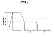
- the melt is kept at a temperature not less than the saturation temperature, and the film is formed in the supercooled melt at the film-forming temperature lower than the saturation temperature.
- the crystallinity of the film is determined by the nature of the above supercooled melt, which is substantially affected by the saturation temperature and the film-forming temperature.
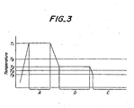
- Fig. 1 and Fig. 3 are graphs schematically showing the temperature schedules of the melts in the novel liquid phase epitaxial process established by the present inventors, respectively.
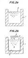
- Figs. 2(a) and 2(b) schematically show the state of the melt in a crucible 1.
- the solute is uniformly molten in the melting medium to form a uniform liquid phase when the substrate is contacted with the melt. Therefore, the appearance of the solid phase occurs at the first time in the whole liquid phase on the surface of the substrate, at the moment that the substrate contacts the melt. Therefore, it is thought that a relatively large nucleation energy is needed to start the growing of the single crystal film.
- the single crystal film starts to grow at the interface between the substrate and the film, the large nucleation energy may cause disorder in the atomic order at the interface.
- the epitaxial film sequentially comes out on the atomic order at the interface and thus the crystallinity thereof may be influenced by the disorder at the interface and degraded.
- the temperature of the liquid phase in the supercooled state may preferably be not higher than 1150°C.
- the film-forming temperature may preferably be not lower than 750°C, because it was rather difficult to form the above solid solution film when applying the film-forming temperature lower than 750°C.
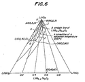
- the inventors tried to produce the films using the melts comprising various compositions shown in figure 5 according to the above film-forming process. Contrary to their expectation, the inventors found that it was possible to stably produce the above solid solution films in a considerably wide range of the compositions.
- the rate of precipitation which solid comes out from the liquid phase needed to be faster than the rate of elusion which lithium niobate is eluted into the liquid phase in the supercooled state.
- the rate of precipitation which solid comes out from the liquid phase needed to be faster than the rate of elusion which lithium niobate is eluted into the liquid phase in the supercooled state.
- the rate of precipitation becomes small. Consequently, the rate of elusion of lithium niobate exceeds the rate of precipitation at a point "F" and the film may not be produced over the point.
- the present inventors adopted the film-forming process as explained referring to Figs. 1 to 3 and successfully produced the film made of the solid solution having a half-value of a X-ray rocking curve smaller than that of the substrate of the optical grade made of lithium niobate single crystal. Then they produced an optical waveguide in the film and evaluated optical properties of the optical waveguide. The inventors found and confirmed that optical damage resistivity of the optical waveguide was conspicuously improved.
- the melt 3 was cooled from T2 to the film-forming temperature T3 lower than T2 by a degree of supercooling ⁇ .
- a substrate 6 of lithium niobate single crystal was contacted with the liquid phase 4 to produce a film.
- the degrees of supercooling ⁇ T were also changed as shown in tables 1 and 2.
- a half-value width of the X-ray rocking curve of each substrate of lithium niobate single crystal of the optical grade used by the inventors was 6.8 to 6.9 (arc sec), and these values were taken as standards for evaluating the crystallinity of the solid solution films.
- Holding temperature T2 (°C) Composition of liquid phase of melt Degree of supecooling ⁇ T (°C) Composition of the film X Half value width (sec) 950 93: 4: 3 15 0.41 5.7 950 88:10: 2 5 0.22 5.6 950 83:16: 1 3 0.10 5.6 1000 93: 3: 4 42 0.68 5.7 1000 90: 6: 4 13 0.36 5.7 1000 80:18: 2 5 0.12 5.8 1050 88: 6: 6 23 0.76 5.6 1050 80:16: 4 6 0.27 5.7 1100 83:10:10: 7 47 0.78 5.8 1100 65:31: 4 7 0.09 5.6 1150 77:14: 9 30 0.65 5.9 1150 65:28: 7 16 0.29 5.9 1200 73:16:11 40 0.76 7.4 1200 65:25:10 30 0.46 7.3 Holding temperature T2 (°C) Composition of liquid phase of melt Degree of supercooling ⁇ T (°C) Composition of the film X
- the solid solution films were produced as in experiment 1. However, the holding temperature T2 and the composition of the liquid phase of the melt were changed as shown in table 5.
- the saturation temperatures were selected to be not more than 1200°C, which were considered to be approvable as can be seen from the results in table 1.
- the content of the melting medium was selected to be 85% which was considered to be approvable as can be seen from the results in the experiments 1 and 2.
- a solid solution film 10 as first layer was formed on the substrate.
- a thickness of the film 10 was 20 ⁇ m and a content "x" of tantalum in the film 10 was 0.35.
- a refractive index of the solid solution film 10 was 2.248 for ordinary ray and 2.194 for extraordinary ray with a wavelength of 633 nm .
- the thus formed second layer 11 may be utilized as an optical waveguide, because the refractive index of the second layer 11 for the ordinary ray is larger than that of the solid solution film 10.
- laser ray with a wavelength of 830 nm was transmitted in the second layer and measured the optical damage resistivity of the second layer 11. Consequently, the optical damage did not occur when applying the laser ray with a irradiation power of 2 mW.
- the solid solution films were formed by the liquid epitaxial process according to the process and the temperature schedule described referring to Fig. 1.
- the films were formed on the substrate of lithium niobate single crystal using the LiNbO 3 -LiTaO 3 -LiVO 3 pseudo-ternary system.
- the charged composition of the melt was adjusted so that a molar ratio of LiNbO 3 :a molar ratio of LiTaO 3 became 80:20.
- a content of LiVO 3 was adjusted so that the saturation temperature T0 of the melt was higher than the film-forming temperature T3 by about 100°C.
- the degree of supercooling ⁇ T was adjusted to 10°C.
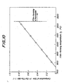
- the film-forming temperatures T3 were variously changed as shown in table 6 and fig.10. Under the condition, the solid solution films were produced and the content of tantalum in each of the thus formed films was measured. These results were shown in table 6 and fig.10. Film-forming temperature T3 (°C) Content of tantalum (x) 809 0.094 875 0.202 941 0.310 1023 0.441 1102 0.563 1167 0.669 1220 0.751
- the film-forming temperature when the film-forming temperature was higher than 1250°C, the solid solution film may not be formed. Because the melting point of the substrate of lithium niobate single crystal is about 1250°C and thus it was impossible to produce the solid solution on the substrate at a temperature over 1250°C. From this viewpoint, the film-forming temperature may preferably be not higher than 1230°C, and the content "x" in the solid solution film became about 0.8 when the temperature was 1230°C.
- the crystallinity of the film was basically same or more superior as that of the film of lithium niobate formed on the substrate of lithium tantalate in the comparative example. It is not clear the reason why the crystallinity of the solid solution film was improved by applying a film-forming temperature not higher than 1150°C. However, a curie temperature of lithium niobate constituting the substrate used is about 1150°C. It is considered that the substrate is converted to multi domain structure and the crystallinity of the substrate was degraded when producing the film at a temperature over 1150°C.
- the inventors provides a method or a technical means to accurately control the content "x" of tantalum in the solid solution film by selecting and controlling the film-forming temperature of the film.
- a method or technical means is extremely useful for producing an optical waveguide of single mode.
- the optical waveguide of single mode in addition to setting a wavelength of light transmitted in the waveguide at a predetermined value and accurately controlling a thickness of the waveguide, it is indispensable to accurately control a refractive index of the waveguide at a predetermined value for propagating the light.
- the permissible range of the refractive index is very narrow.
- the inventors studied a manufacturing process for maintaining the excellent propagation property of the optical waveguide of the single mode based on the above discovery.
- an optical waveguide was formed in each solid solution film by a so called proton exchange process under the same condition.
- mask patterns made of aluminum each having a width of 2 ⁇ m were formed on the surface of each film by conventional photolithography method to provide an assembly, which was then dipped in benzoic acid of 200°C for 15 minutes to form the waveguide.
- the mask patterns were removed by etching process and the waveguide was subjected to an annealing process at 350°C for 4 hours to provide a substrate with a proton-exchange optical waveguide.
- Light of a wavelength of 830 nm was irradiated to the optical waveguide of each example and the propagation loss was measured.
Landscapes
- Chemical & Material Sciences (AREA)
- Engineering & Computer Science (AREA)
- Crystallography & Structural Chemistry (AREA)
- Materials Engineering (AREA)
- Metallurgy (AREA)
- Organic Chemistry (AREA)
- Inorganic Chemistry (AREA)
- Crystals, And After-Treatments Of Crystals (AREA)
Claims (6)
- Gegenstand, umfassend ein Einkristallsubstrat (6) mit der Zusammensetzung LiNb1-zTazO3, worin gilt: 0 ≤ z < 0,8, einen nach einem Flüssigphasen-Epitaxieverfahren auf dem Substrat ausgebildeten ersten Film (10) aus einer festen Lithiumniobat-Lithiumtantalat-Lösung, sowie einen auf dem ersten Film (10) ausgebildeten und aus einer festen Lithiumniobat-Lithiumtantalat-Lösung bestehenden zweiten Film (11), worin der erste Film (10) die Zusammensetzung LiNb1-xTaxO3 umfasst, worin gilt: 0 < x ≤ 0,8 und z < x, und der zweite Film (11) die Zusammensetzung LiNb1-yTayO3 umfasst, worin gilt: 0 ≤ y < 0,8 und y < x.
- Gegenstand nach Anspruch 1, worin x nicht kleiner als 0,02 ist.
- Gegenstand nach Anspruch 1 oder 2, worin das Einkristallsubstrat (6) und der erste Film (10) ein oder mehrere Seltenerdelement(e) enthalten.
- Gegenstand nach Anspruch 3, worin das oder die Seltenerdelement(e) eines oder mehrere von Nd, Er, Tm, Ho, Dy und Pr ist bzw. sind.
- Gegenstand nach Anspruch 1 oder 2, worin das Substrat (6) und der erste Film (10) ein oder mehrere Metallelement(e), ausgewählt aus der aus Zink, Scandium, Magnesium, Indium, Titan und Vanadium bestehenden Gruppe, enthalten.
- Gegenstand nach einem der Ansprüche 1 bis 5, worin die Halbwertsbreite einer Röntgenstrahlen-Rocking-Kurve des ersten Films nicht größer ist als jene des Substrats.
Applications Claiming Priority (6)
| Application Number | Priority Date | Filing Date | Title |
|---|---|---|---|
| JP22208194 | 1994-09-16 | ||
| JP222081/94 | 1994-09-16 | ||
| JP22208194 | 1994-09-16 | ||
| JP8393995 | 1995-04-10 | ||
| JP8393995 | 1995-04-10 | ||
| JP83939/95 | 1995-04-10 |
Publications (3)
| Publication Number | Publication Date |
|---|---|
| EP0707096A2 EP0707096A2 (de) | 1996-04-17 |
| EP0707096A3 EP0707096A3 (de) | 1997-03-05 |
| EP0707096B1 true EP0707096B1 (de) | 2001-10-17 |
Family
ID=26424977
Family Applications (1)
| Application Number | Title | Priority Date | Filing Date |
|---|---|---|---|
| EP95303946A Expired - Lifetime EP0707096B1 (de) | 1994-09-16 | 1995-06-08 | Einkristallssubstrat enthaltende Gegenstände |
Country Status (3)
| Country | Link |
|---|---|
| US (1) | US5650006A (de) |
| EP (1) | EP0707096B1 (de) |
| DE (1) | DE69523252T2 (de) |
Families Citing this family (5)
| Publication number | Priority date | Publication date | Assignee | Title |
|---|---|---|---|---|
| JPH0987085A (ja) * | 1995-09-22 | 1997-03-31 | Ngk Insulators Ltd | 光学単結晶品および光学素子 |
| JPH1082921A (ja) * | 1996-09-06 | 1998-03-31 | Ngk Insulators Ltd | 光導波路基板、光導波路部品、第二高調波発生デバイスおよび光導波路基板の製造方法 |
| US6673330B1 (en) * | 1999-03-26 | 2004-01-06 | National Institute For Research In Inorganic Materials | Single crystal of lithium niobate or tantalate and its optical element, and process and apparatus for producing an oxide single crystal |
| JP3938147B2 (ja) * | 2003-04-08 | 2007-06-27 | 住友金属鉱山株式会社 | タンタル酸リチウム基板およびその製造方法 |
| CN114725354A (zh) * | 2022-04-29 | 2022-07-08 | 远景动力技术(江苏)有限公司 | 正极材料及其应用 |
Citations (1)
| Publication number | Priority date | Publication date | Assignee | Title |
|---|---|---|---|---|
| EP0674027A1 (de) * | 1994-03-25 | 1995-09-27 | Ngk Insulators, Ltd. | Optoelektrische Gegenstände und Verfahren zu ihrer Herstellung |
Family Cites Families (3)
| Publication number | Priority date | Publication date | Assignee | Title |
|---|---|---|---|---|
| US3998687A (en) * | 1975-03-10 | 1976-12-21 | Bell Telephone Laboratories, Incorporated | Technique for growth of thin film lithium niobate by liquid phase epitaxy |
| US4073675A (en) * | 1976-07-21 | 1978-02-14 | Bell Telephone Laboratories, Incorporated | Waveguiding epitaxial LiNbO3 films |
| US5209917A (en) * | 1989-09-20 | 1993-05-11 | Ibiden Co., Ltd. | Lithium niobate single crystal thin film and production method thereof |
-
1995
- 1995-06-07 US US08/473,964 patent/US5650006A/en not_active Expired - Lifetime
- 1995-06-08 DE DE69523252T patent/DE69523252T2/de not_active Expired - Lifetime
- 1995-06-08 EP EP95303946A patent/EP0707096B1/de not_active Expired - Lifetime
Patent Citations (1)
| Publication number | Priority date | Publication date | Assignee | Title |
|---|---|---|---|---|
| EP0674027A1 (de) * | 1994-03-25 | 1995-09-27 | Ngk Insulators, Ltd. | Optoelektrische Gegenstände und Verfahren zu ihrer Herstellung |
Also Published As
| Publication number | Publication date |
|---|---|
| US5650006A (en) | 1997-07-22 |
| DE69523252D1 (de) | 2001-11-22 |
| EP0707096A3 (de) | 1997-03-05 |
| DE69523252T2 (de) | 2002-07-11 |
| EP0707096A2 (de) | 1996-04-17 |
Similar Documents
| Publication | Publication Date | Title |
|---|---|---|
| EP0515682B1 (de) | Dünner film eines lithiumniobat-einkristalls | |
| EP0444209B1 (de) | Dünnfilmeinzelkristall aus lithiumniobat und verfahren zu seiner herstellung | |
| EP0707096B1 (de) | Einkristallssubstrat enthaltende Gegenstände | |
| US3998687A (en) | Technique for growth of thin film lithium niobate by liquid phase epitaxy | |
| EP0768393B1 (de) | Optische einkristalline Gegenstände und ihre Verwendung zur Herstellung optischer Bauelemente | |
| US5985022A (en) | Optoelectric articles and a process for producing the same | |
| US5539569A (en) | Optoelectric articles and a process for producing the same | |
| Adachi et al. | Epitaxial growth of potassium lithium niobate single-crystal films for optical-waveguides | |
| JP3725589B2 (ja) | 単結晶基板品、光部品、単結晶基板品の製造方法および光部品の製造方法 | |
| Bohac et al. | KTN optical waveguides grown by liquid-phase epitaxy | |
| US5517942A (en) | Process for producing optoelectric articles | |
| JP2951583B2 (ja) | 光導波路部品、第二高調波発生デバイスおよび光導波路部品の製造方法 | |
| JP3348129B2 (ja) | 電気光学品の製造方法 | |
| JPH05896A (ja) | ニオブ酸リチウム単結晶薄膜 | |
| JPH0369586A (ja) | ニオブ酸リチウム単結晶薄膜の製造方法 | |
| EP0686711B1 (de) | Verfahren zur herstellung einer magneto-optische vorrichtung | |
| JPH0664996A (ja) | ニオブ酸リチウム単結晶薄膜の製造方法 | |
| JPH05229897A (ja) | ニオブ酸リチウム単結晶薄膜とその製造方法 | |
| JP3096747B2 (ja) | チャンネル型光導波路の形成方法 | |
| JPH08292459A (ja) | 第二高調波発生素子およびその製造方法 | |
| JPH0412094A (ja) | ニオブ酸リチウム単結晶薄膜 | |
| JPH09100200A (ja) | 単結晶エピタキシャル膜、単結晶品および第二高調波発生素子 | |
| JPH0891986A (ja) | 単結晶基板品の製造方法 | |
| JPH05178692A (ja) | ニオブ酸リチウム単結晶薄膜 | |
| JPH06157198A (ja) | Ti含有ニオブ酸リチウム薄膜及びその製造方法 |
Legal Events
| Date | Code | Title | Description |
|---|---|---|---|
| PUAI | Public reference made under article 153(3) epc to a published international application that has entered the european phase |
Free format text: ORIGINAL CODE: 0009012 |
|
| AK | Designated contracting states |
Kind code of ref document: A2 Designated state(s): DE FR GB |
|
| PUAL | Search report despatched |
Free format text: ORIGINAL CODE: 0009013 |
|
| AK | Designated contracting states |
Kind code of ref document: A3 Designated state(s): DE FR GB |
|
| 17P | Request for examination filed |
Effective date: 19970314 |
|
| 17Q | First examination report despatched |
Effective date: 19990226 |
|
| RTI1 | Title (correction) |
Free format text: ARTICLES COMPRISING A SUBSTRATE MADE OF SINGLE CRYSTAL |
|
| GRAG | Despatch of communication of intention to grant |
Free format text: ORIGINAL CODE: EPIDOS AGRA |
|
| GRAG | Despatch of communication of intention to grant |
Free format text: ORIGINAL CODE: EPIDOS AGRA |
|
| GRAH | Despatch of communication of intention to grant a patent |
Free format text: ORIGINAL CODE: EPIDOS IGRA |
|
| GRAH | Despatch of communication of intention to grant a patent |
Free format text: ORIGINAL CODE: EPIDOS IGRA |
|
| GRAA | (expected) grant |
Free format text: ORIGINAL CODE: 0009210 |
|
| AK | Designated contracting states |
Kind code of ref document: B1 Designated state(s): DE FR GB |
|
| REF | Corresponds to: |
Ref document number: 69523252 Country of ref document: DE Date of ref document: 20011122 |
|
| REG | Reference to a national code |
Ref country code: GB Ref legal event code: IF02 |
|
| ET | Fr: translation filed | ||
| PLBE | No opposition filed within time limit |
Free format text: ORIGINAL CODE: 0009261 |
|
| STAA | Information on the status of an ep patent application or granted ep patent |
Free format text: STATUS: NO OPPOSITION FILED WITHIN TIME LIMIT |
|
| 26N | No opposition filed | ||
| PGFP | Annual fee paid to national office [announced via postgrant information from national office to epo] |
Ref country code: GB Payment date: 20140604 Year of fee payment: 20 |
|
| PGFP | Annual fee paid to national office [announced via postgrant information from national office to epo] |
Ref country code: DE Payment date: 20140603 Year of fee payment: 20 |
|
| PGFP | Annual fee paid to national office [announced via postgrant information from national office to epo] |
Ref country code: FR Payment date: 20140609 Year of fee payment: 20 |
|
| REG | Reference to a national code |
Ref country code: DE Ref legal event code: R071 Ref document number: 69523252 Country of ref document: DE |
|
| REG | Reference to a national code |
Ref country code: GB Ref legal event code: PE20 Expiry date: 20150607 |
|
| PG25 | Lapsed in a contracting state [announced via postgrant information from national office to epo] |
Ref country code: GB Free format text: LAPSE BECAUSE OF EXPIRATION OF PROTECTION Effective date: 20150607 |