EP0708372A1 - Procédé de décollage à une seule couche de photoréserve pour former des motifs sur un support - Google Patents
Procédé de décollage à une seule couche de photoréserve pour former des motifs sur un support Download PDFInfo
- Publication number
- EP0708372A1 EP0708372A1 EP95305923A EP95305923A EP0708372A1 EP 0708372 A1 EP0708372 A1 EP 0708372A1 EP 95305923 A EP95305923 A EP 95305923A EP 95305923 A EP95305923 A EP 95305923A EP 0708372 A1 EP0708372 A1 EP 0708372A1
- Authority
- EP
- European Patent Office
- Prior art keywords
- resist
- substrate
- resist layer
- minutes
- layer
- Prior art date
- Legal status (The legal status is an assumption and is not a legal conclusion. Google has not performed a legal analysis and makes no representation as to the accuracy of the status listed.)
- Granted
Links
- 238000000034 method Methods 0.000 title claims abstract description 82
- 230000008569 process Effects 0.000 title claims abstract description 80
- 239000000758 substrate Substances 0.000 title claims abstract description 67
- MVPPADPHJFYWMZ-UHFFFAOYSA-N chlorobenzene Chemical compound ClC1=CC=CC=C1 MVPPADPHJFYWMZ-UHFFFAOYSA-N 0.000 claims abstract description 36
- 229910052751 metal Inorganic materials 0.000 claims description 44
- 239000002184 metal Substances 0.000 claims description 44
- 239000000463 material Substances 0.000 claims description 20
- CSCPPACGZOOCGX-UHFFFAOYSA-N Acetone Chemical compound CC(C)=O CSCPPACGZOOCGX-UHFFFAOYSA-N 0.000 claims description 18
- 238000000151 deposition Methods 0.000 claims description 17
- 239000003849 aromatic solvent Substances 0.000 claims description 14
- 230000008021 deposition Effects 0.000 claims description 14
- 238000010438 heat treatment Methods 0.000 claims description 13
- 229920002120 photoresistant polymer Polymers 0.000 claims description 13
- 239000002904 solvent Substances 0.000 claims description 9
- 229910052804 chromium Inorganic materials 0.000 claims description 5
- 229910001218 Gallium arsenide Inorganic materials 0.000 claims description 4
- 238000013019 agitation Methods 0.000 claims description 4
- 229920005989 resin Polymers 0.000 claims description 4
- 239000011347 resin Substances 0.000 claims description 4
- 229910052737 gold Inorganic materials 0.000 claims description 3
- 229910052759 nickel Inorganic materials 0.000 claims description 3
- 229910052697 platinum Inorganic materials 0.000 claims description 3
- 230000005855 radiation Effects 0.000 claims description 3
- 229910052715 tantalum Inorganic materials 0.000 claims description 3
- 229910052719 titanium Inorganic materials 0.000 claims description 3
- 229910003327 LiNbO3 Inorganic materials 0.000 claims description 2
- 229910045601 alloy Inorganic materials 0.000 claims description 2
- 239000000956 alloy Substances 0.000 claims description 2
- 239000000203 mixture Substances 0.000 claims description 2
- 229920003986 novolac Polymers 0.000 claims description 2
- 239000012780 transparent material Substances 0.000 claims description 2
- 238000001465 metallisation Methods 0.000 abstract description 35
- 238000004519 manufacturing process Methods 0.000 description 7
- 230000000052 comparative effect Effects 0.000 description 5
- 238000012545 processing Methods 0.000 description 5
- 239000000126 substance Substances 0.000 description 5
- VYZAMTAEIAYCRO-UHFFFAOYSA-N Chromium Chemical compound [Cr] VYZAMTAEIAYCRO-UHFFFAOYSA-N 0.000 description 4
- PXHVJJICTQNCMI-UHFFFAOYSA-N Nickel Chemical compound [Ni] PXHVJJICTQNCMI-UHFFFAOYSA-N 0.000 description 4
- 239000011651 chromium Substances 0.000 description 4
- 238000010586 diagram Methods 0.000 description 4
- 150000002739 metals Chemical class 0.000 description 4
- BASFCYQUMIYNBI-UHFFFAOYSA-N platinum Chemical compound [Pt] BASFCYQUMIYNBI-UHFFFAOYSA-N 0.000 description 4
- 229910052782 aluminium Inorganic materials 0.000 description 3
- XAGFODPZIPBFFR-UHFFFAOYSA-N aluminium Chemical compound [Al] XAGFODPZIPBFFR-UHFFFAOYSA-N 0.000 description 3
- 230000003287 optical effect Effects 0.000 description 3
- RTAQQCXQSZGOHL-UHFFFAOYSA-N Titanium Chemical compound [Ti] RTAQQCXQSZGOHL-UHFFFAOYSA-N 0.000 description 2
- 238000010521 absorption reaction Methods 0.000 description 2
- 238000004873 anchoring Methods 0.000 description 2
- 238000004140 cleaning Methods 0.000 description 2
- 238000011161 development Methods 0.000 description 2
- 230000000694 effects Effects 0.000 description 2
- 238000005530 etching Methods 0.000 description 2
- 230000008020 evaporation Effects 0.000 description 2
- 238000001704 evaporation Methods 0.000 description 2
- PCHJSUWPFVWCPO-UHFFFAOYSA-N gold Chemical compound [Au] PCHJSUWPFVWCPO-UHFFFAOYSA-N 0.000 description 2
- 239000010931 gold Substances 0.000 description 2
- 230000004048 modification Effects 0.000 description 2
- 238000012986 modification Methods 0.000 description 2
- 238000004886 process control Methods 0.000 description 2
- 238000002791 soaking Methods 0.000 description 2
- GUVRBAGPIYLISA-UHFFFAOYSA-N tantalum atom Chemical compound [Ta] GUVRBAGPIYLISA-UHFFFAOYSA-N 0.000 description 2
- 239000010936 titanium Substances 0.000 description 2
- 239000000654 additive Substances 0.000 description 1
- 230000000996 additive effect Effects 0.000 description 1
- 238000000637 aluminium metallisation Methods 0.000 description 1
- 238000013459 approach Methods 0.000 description 1
- 230000004888 barrier function Effects 0.000 description 1
- 230000005540 biological transmission Effects 0.000 description 1
- 230000015572 biosynthetic process Effects 0.000 description 1
- 230000008859 change Effects 0.000 description 1
- 238000003486 chemical etching Methods 0.000 description 1
- 238000005229 chemical vapour deposition Methods 0.000 description 1
- 239000011248 coating agent Substances 0.000 description 1
- 238000000576 coating method Methods 0.000 description 1
- 238000006482 condensation reaction Methods 0.000 description 1
- 230000001419 dependent effect Effects 0.000 description 1
- 238000009792 diffusion process Methods 0.000 description 1
- 239000006185 dispersion Substances 0.000 description 1
- 238000004090 dissolution Methods 0.000 description 1
- 238000010894 electron beam technology Methods 0.000 description 1
- 238000005516 engineering process Methods 0.000 description 1
- 230000008570 general process Effects 0.000 description 1
- 239000011521 glass Substances 0.000 description 1
- 239000012535 impurity Substances 0.000 description 1
- 230000006698 induction Effects 0.000 description 1
- 238000003754 machining Methods 0.000 description 1
- 230000007246 mechanism Effects 0.000 description 1
- 239000002905 metal composite material Substances 0.000 description 1
- 230000035515 penetration Effects 0.000 description 1
- 238000000206 photolithography Methods 0.000 description 1
- 238000001020 plasma etching Methods 0.000 description 1
- 238000003908 quality control method Methods 0.000 description 1
- 239000013557 residual solvent Substances 0.000 description 1
- 238000004544 sputter deposition Methods 0.000 description 1
- XLYOFNOQVPJJNP-UHFFFAOYSA-N water Substances O XLYOFNOQVPJJNP-UHFFFAOYSA-N 0.000 description 1
- 238000003079 width control Methods 0.000 description 1
Images


Classifications
-
- G—PHYSICS
- G03—PHOTOGRAPHY; CINEMATOGRAPHY; ANALOGOUS TECHNIQUES USING WAVES OTHER THAN OPTICAL WAVES; ELECTROGRAPHY; HOLOGRAPHY
- G03F—PHOTOMECHANICAL PRODUCTION OF TEXTURED OR PATTERNED SURFACES, e.g. FOR PRINTING, FOR PROCESSING OF SEMICONDUCTOR DEVICES; MATERIALS THEREFOR; ORIGINALS THEREFOR; APPARATUS SPECIALLY ADAPTED THEREFOR
- G03F7/00—Photomechanical, e.g. photolithographic, production of textured or patterned surfaces, e.g. printing surfaces; Materials therefor, e.g. comprising photoresists; Apparatus specially adapted therefor
- G03F7/16—Coating processes; Apparatus therefor
- G03F7/168—Finishing the coated layer, e.g. drying, baking, soaking
-
- G—PHYSICS
- G03—PHOTOGRAPHY; CINEMATOGRAPHY; ANALOGOUS TECHNIQUES USING WAVES OTHER THAN OPTICAL WAVES; ELECTROGRAPHY; HOLOGRAPHY
- G03F—PHOTOMECHANICAL PRODUCTION OF TEXTURED OR PATTERNED SURFACES, e.g. FOR PRINTING, FOR PROCESSING OF SEMICONDUCTOR DEVICES; MATERIALS THEREFOR; ORIGINALS THEREFOR; APPARATUS SPECIALLY ADAPTED THEREFOR
- G03F7/00—Photomechanical, e.g. photolithographic, production of textured or patterned surfaces, e.g. printing surfaces; Materials therefor, e.g. comprising photoresists; Apparatus specially adapted therefor
- G03F7/26—Processing photosensitive materials; Apparatus therefor
- G03F7/40—Treatment after imagewise removal, e.g. baking
-
- G—PHYSICS
- G03—PHOTOGRAPHY; CINEMATOGRAPHY; ANALOGOUS TECHNIQUES USING WAVES OTHER THAN OPTICAL WAVES; ELECTROGRAPHY; HOLOGRAPHY
- G03F—PHOTOMECHANICAL PRODUCTION OF TEXTURED OR PATTERNED SURFACES, e.g. FOR PRINTING, FOR PROCESSING OF SEMICONDUCTOR DEVICES; MATERIALS THEREFOR; ORIGINALS THEREFOR; APPARATUS SPECIALLY ADAPTED THEREFOR
- G03F7/00—Photomechanical, e.g. photolithographic, production of textured or patterned surfaces, e.g. printing surfaces; Materials therefor, e.g. comprising photoresists; Apparatus specially adapted therefor
- G03F7/26—Processing photosensitive materials; Apparatus therefor
- G03F7/42—Stripping or agents therefor
- G03F7/422—Stripping or agents therefor using liquids only
-
- H—ELECTRICITY
- H05—ELECTRIC TECHNIQUES NOT OTHERWISE PROVIDED FOR
- H05K—PRINTED CIRCUITS; CASINGS OR CONSTRUCTIONAL DETAILS OF ELECTRIC APPARATUS; MANUFACTURE OF ASSEMBLAGES OF ELECTRICAL COMPONENTS
- H05K3/00—Apparatus or processes for manufacturing printed circuits
- H05K3/10—Apparatus or processes for manufacturing printed circuits in which conductive material is applied to the insulating support in such a manner as to form the desired conductive pattern
- H05K3/14—Apparatus or processes for manufacturing printed circuits in which conductive material is applied to the insulating support in such a manner as to form the desired conductive pattern using spraying techniques to apply the conductive material, e.g. vapour evaporation
- H05K3/143—Masks therefor
Definitions
- the present invention relates to a single resist layer lift-off process for forming patterned layers on a substrate.
- the process provides a patterned resist layer having improved resist profile overhang and negative slope in the sidewalls of the resist profile, which collectively increase production yield and reduce production time and expense.
- Lift-off processing is often referred to as an "additive" process in contrast to the more typical use of a photoresist mask where the areas of desired metallization are protected and the undesired areas are left exposed and etched away using appropriate chemicals.
- the substrate is covered by photoresist everywhere except in areas where the metallization is desired.
- the metal is then added, covering the entire substrate with the metal sitting on top of the photoresist and in contact with the substrate in the open areas.
- the photoresist is subsequently removed lifting the unwanted metal away from the substrate, leaving behind the desired metal pattern.
- the impetus for the lift-off process was the need to pattern metal lines on substrates where the use of chemical or plasma etching is either undesirable or incompatible with the process or materials involved.
- An example of this is in the processing of GaAs substrates.
- Typical metallization schemes require the use of a metal composites to form contacts and transmission lines.
- Typical metals used are aluminum, gold, nickel, chromium, platinum, tantalum, titanium and others, where the required contacts may use two or three layers of these metals in some combination. Etching these metals would require very harsh chemicals that would severely attack the GaAs substrate and degrade the performance of the device.
- the lift-off process was first introduced as a "brute force" processing technique.
- the idea was to deposit a thin metal coating 3 ( ⁇ 0.2 ⁇ m) over a thick ( ⁇ 2 ⁇ m) photoresist pattern 2, and then force the metal to make a clean break as shown in Figure 1.
- This idealized process is not practical.
- the process requires the metal to be delivered normal to the surface of the substrate 1. The best approximation to this situation would occur in an evaporator.
- the metal "melt” is kept in a water cooled crucible inside an evacuated chamber (typically in the 10 ⁇ 6 to 10 ⁇ 8 Torr range) where an electron beam is directed via a magnetic field to impinge on the metal surface, heating the metal in a controlled manner. Due to the elevated temperature of the metal melt, a vapor pressure is created allowing the metal atoms to diffuse throughout the chamber, as if from a point source.
- the metal atoms tend to arrive normal to the surface.
- certain constraints tend to limit the realization of this phenomena. Wafer surfaces tend to be quite large, ranging from 3 to 8 inches in diameter, so only a small portion can be tangent to the required curve. Practical considerations also tend to limit the source to wafer distance to under a meter with machining tolerances and quality control in the assembly of commercially available equipment, all making an ideal evaporation impossible to achieve on a production scale.
- Sputtering which is more conformed than evaporation and chemical vapor deposition of metallic films, will completely cover the photoresist and impede its removal. If the photoresist overhang profile is poor the deposited metal will adhere together with the photoresist sidewall making it difficult to perform lift-off and resulting in rough metal line quality.
- the second major obstacle to the brute force approach is the resist profile itself. Because photolithography is an optical process, it is subject to optical constraints. The light (board band or monochromatic) will be absorbed as it passes through the resist layer causing the top of the film to receive a higher dose of energy than the bottom, thus making the top layer of the resist more soluble in the developer. This produces resist profiles that instead of being at right angles to the substrate, form more rounded profiles, larger at the bottom and smaller at the top, defined as a positive slope as shown in Fig. 5a.
- diffraction In addition to absorption, diffraction also plays a significant role in creating positive slope in the sidewalls of the resist profile allowing the light to spread out and expose a larger area at the surface of the resist. Diffraction effects become greatest when the mask is not in physical contact with the resist, a typical requirement in order to avoid damaging the mask and the wafer. As the gap between the mask and resist increases, the profile becomes quite rounded (Fig. 5b) and resolution is reduced.
- the positive photoresist is exposed in the usual manner and then soaked in an aromatic solvent, typically chlorobenzene. It is known that the penetration of the solvent into the resist, which defines the depth of the overhang profile, is controlled by the soaking time, solvent content after soft bake, developer concentrations, temperature and impurities in the chlorobenzene. See JP 60-32047 and Chem. Abst. 103-62591.
- the previously exposed areas of the resist, where penetrated by chlorobenzene tend to dissolve slower than the unpenetrated areas.
- the unpenetrated resist is over-developed, resulting in an undercut resist profile, shown theoretically in Fig. 5c.
- the IBM process is shown in flow diagram form in Fig. 6. Although this process has been widely adopted in industry, in production it is very difficult to control. Tight process controls must be observed during soft bake, soak, development and exposure. A small variation in any one of the many variables present in each of these steps will result in reduced production yield, increased production time and increased production expense. Additionally, when the resist is exposed before the chlorobenzene soak, different regions of exposed and unexposed resist have different solubilities to the chlorobenzene. Consequently, it is difficult to diffuse the chlorobenzene uniformly over the surface of the resist.
- the process of the present invention comprises the steps of depositing a single resist layer on an upper surface of a substrate to form a resist/substrate preform; subjecting the resist/substrate preform to a first heat treatment to adhere the resist layer to the substrate; immersing the resist/substrate preform in a bath of aromatic solvent; subjecting the resist/substrate preform to a second heat treatment; exposing portions of the resist layer in the shape of a pattern; developing the resist layer to remove exposed portions thereof and form a patterned resist layer wherein openings are provided through the resist layer to the upper surface of the substrate; applying a layer of deposition material on the patterned resist layer and through the openings therein to form a desired pattern of material on the upper surface of the substrate; and immersing the substrate, with the patterned resist layer and deposition material formed thereon, in a solvent bath to lift-off the patterned resist layer, with the deposition material formed thereon, while leaving tee pattern of material on the upper surface of the substrate.
- Fig. 7 is a flow diagram showing the general process steps of the present invention.
- the process begins with a standard solvent cleaning of the substrate 1.
- a specific application of the process of the present invention is in the formation of metallized layers on integrated optic devices.
- the substrate can comprise a transparent material such as GaAs or LiNbO3.
- a resist layer 2 is then formed on an upper surface of the substrate 1 and subjected to a soft bake to adhere the resist to the substrate and control the thickness of the resist layer 2.
- the soft bake can range in temperature from 80-100°C for about 10-30 minutes, but is preferably performed at about 90°C for about 20 minutes.
- the entire substrate and resist layer (resist/substrate preform) is then soaked in an aromatic solvent, preferably chlorobenzene, for about 5-25 minutes, preferably 10-20 minutes, more preferably about 15 minutes. Since the resist layer contains novolak resins formed by a condensation reaction, the molecular weight dispersivity of the resins is very broad, ranging from 30 to 2000. When soaking the resist coated substrate in the aromatic solvent, the low molecular weight resins and photoactive components are preferentially removed. The absorption of the aromatic solvent at the top surface of the resist also retards dissolution of that resist in the developer solution, and thus contributes to providing increased overhang in the resist profile. That portion of the resist layer which is not penetrated by the aromatic solvent retains its original solubility.
- an aromatic solvent preferably chlorobenzene
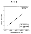
- Fig. 8 shows the change in overhang length dependent upon chlorobenzene soak time.
- a post-soak bake is employed after the aromatic solvent soak to control the dispersion of aromatic solvent into the resist layer. More specifically, after the entire unexposed resist/substrate preform is soaked in the aromatic solvent, the post-soak baking step is performed to remove any residual solvent in the resist. This baking step thus prevents any further undesired in-diffusion of aromatic solvent into the resist layer. The aromatic solvent thus diffuses into the top layer of the resist forming a consistent induction layer, which in turn provides a more pronounced resist profile overhang.
- the post-soak bake also forms a negative profile in the sidewalls of the resist profile (Fig. 9).
- the post-soak baking of the present invention is performed at a temperature ranging from 80-100°C for about 5-15 minutes. More preferably, the post-soak bake is performed at about 90° for about 10 minutes.
- the resist layer is then exposed through a mask to define therein the outline of the desired pattern.
- the exposure step uses standard UV radiation technology and is carried out for about 5-15 seconds, more preferably about 7.5 seconds, when using a LiNb03 substrate at 13.6 mW lamp intensity.
- the resist is then developed by immersion in a standard developing chemical (e.g., Shiply Miroposit 303A) for about 15 seconds, to form a patterned resist having a latent image of the desired pattern to be formed on the substrate.
- a standard developing chemical e.g., Shiply Miroposit 303A
- the next step in the process is to deposit the material for forming the pattern on the substrate.
- an aspect ratio of resist layer thickness to deposition material thickness of approximately 2:1 is preferred.
- metal is used in the explanation herein, it is understood that other materials could also be used to form the pattern (e.g., resistive materials, glass materials, and the like).
- the metal 3 is deposited over the entire upper surface of the resist and on those portions of the upper surface of the substrate which are exposed through the resist. Although any type of metal can be deposited, the most common metals used include aluminum, gold, chromium, nickel, platinum, tantalum, titanium, mixtures thereof and alloys thereof.
- the substrate should be subjected to a post-metallization bake.
- a post-metallization bake makes the resist layer firmer, and thus easier to lift-off, and also assists in providing the sidewalls of the resist profile with improved negative slope as shown in Fig. 9.
- the post-metallization bake is performed in a temperature ranging from about 100°C to about 140°C for about 15-35 minutes. More preferably the post-metallization bake is performed at 110-130°C for 20-30 minutes, and most preferably at about 120°C for about 25 minutes.
- the entire substrate, with the resist layer and metallization layer formed thereon is immersed in an acetone bath and subjected to ultrasonic agitation to lift-off the resist layer and that portion of the metallization layer formed thereon, thus leaving the substrate 1 with the desired metallization pattern 3 formed thereon.
- the resist sidewall is not metallized due to non-normal (i.e., non-perpendicular) application of deposition metal onto the substrate.
- the fact that the present process provides the sidewalls of the resist profile with a negative slope also prevents the deposition of metal (especially when depositing consecutive layers of relatively thick metal) onto the sidewalls of the resist during the metaliization step.
- a transparent substrate of LiNb03 was subjected to a conventional solvent cleaning, and then an AZ1350J resist layer was formed on an upper surface of the substrate using a coater at a spin speed of 3000 rpm.
- the resist was then soft baked at 90°C for 20 minutes and immersed in a chlorobenzene bath for a soak time of 15 minutes.
- the resist/substrate preform was then post-soak baked at 90°C for 10 minutes.
- Fig. 10a shows the resist profile of the patterned resist layer and Fig. 10b shows magnified end portions of the resist profile shown in Fig. 10a.
- the resist profile has an overhang length of about 0.4 ⁇ m.
- the wafer was then loaded in a Temescal VES-2550 evaporator to deposit, on the substrate through the openings in the resist layer, a first metallization layer of chromium to a thickness of 200 ⁇ and, on the first layer, a second metallization layer of aluminum to a thickness of 9900 ⁇ .
- the wafer was then post-metallization baked at 120°C for 25 minutes. This baking step makes the resist layer firmer and also assists in providing the sidewalls of the resist profile with improved negative slope.
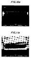
- Figs. 11a and 11b are SEM photographs showing the resist profile and deposited metal layer formed in accordance with this example.
- Fig. 11b shows the opposite sides of the structure of Fig. 11a at an increased magnification.
- Figs. 11a and 11b clearly show that the sidewall of the resist profile has a negative slope and the overhang of the resist profile is pronounced. Consequently, Figs. 11a and 11b also show that metallization of the sidewall of the resist does not occur, and thus the lift-off step in accordance with the present invention can be performed in about 15 minutes, because the acetone can freely access the resist (Fig. 11b) and no metal exists between the metallization layer on the surface of the substrate and the metallization layer on the upper surface of the resist, which would otherwise result in anchoring the resist to the substrate.
- the wafer was then immersed in acetone for 10 minutes and subjected to ultrasonic agitation.
- the acetone was changed and the step was continued for an additional 5 minutes to achieve complete lift-off of the resist layer and metallization layer formed thereon.
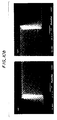
- Figs. 12a and 12b show the line quality of the metallized pattern formed in accordance with the present invention.
- Fig. 12 b is a magnified portion of Fig. 12a.
- Fig. 13 also shows the superior line quality of the metallization pattern formed according to the present invention.
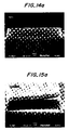
- Fig. 14a shows the resist profile of the patterned resist layer formed by the prior art process
- Fig. 14b includes magnified end portions of the resist profile shown in Fig. 14a.
- the resist profile has an overhang length of only about 0.1 ⁇ m. Accordingly, comparing Figs. 10a and 10b to Figs. 14a and 14b, respectively, it can seen that the resist profile formed in accordance with the process of the present invention has negative slope in the sidewalls thereof and improved overhang length, when compared to the resist profile formed in accordance with the prior art process.
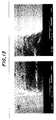
- Figs. 15a and 15b show the resist profile and deposited metal layer formed in accordance with the prior art process of this comparative example.
- Fig. 15b shows the opposite sides of the structure of Fig. 15a at an increased magnification.
- Figs. 15a and 15b clearly show that metallization of the resist sidewall occurs. Such metallization of the resist sidewalls inhibits access of the acetone to the resist layer and also acts as an anchor between the metallized layer on top of the resist layer and the metallized layer on the substrate surface. Accordingly, it took nearly 8 hours to lift-off the resist layer formed in accordance with the prior art process of this comparative example.
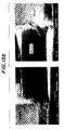
- Figs. 16a and 16b show the line quality of the metallized pattern formed in accordance with the prior art process of this comparative example.
- Fig. 16b is a magnified portion of Fig. 16a.
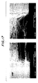
- Fig. 17 also shows the line quality of the metallization pattern formed according to the prior art process.
- FIG. 12a, 12b and 13 A comparison between Figs. 12a, 12b and 13, and Figs. 16a, 16b and 17, respectively, shows that the line quality of the metallized pattern is improved when formed in accordance with the process of the present invention.
Landscapes
- Physics & Mathematics (AREA)
- General Physics & Mathematics (AREA)
- Photosensitive Polymer And Photoresist Processing (AREA)
- Weting (AREA)
- Manufacturing Of Printed Circuit Boards (AREA)
- Exposure Of Semiconductors, Excluding Electron Or Ion Beam Exposure (AREA)
Applications Claiming Priority (2)
| Application Number | Priority Date | Filing Date | Title |
|---|---|---|---|
| US325164 | 1989-03-17 | ||
| US32516494A | 1994-10-21 | 1994-10-21 |
Publications (2)
| Publication Number | Publication Date |
|---|---|
| EP0708372A1 true EP0708372A1 (fr) | 1996-04-24 |
| EP0708372B1 EP0708372B1 (fr) | 2000-03-22 |
Family
ID=23266714
Family Applications (1)
| Application Number | Title | Priority Date | Filing Date |
|---|---|---|---|
| EP95305923A Expired - Lifetime EP0708372B1 (fr) | 1994-10-21 | 1995-08-24 | Procédé de décollage à une seule couche de photoréserve pour former des motifs sur un support |
Country Status (4)
| Country | Link |
|---|---|
| US (1) | US5654128A (fr) |
| EP (1) | EP0708372B1 (fr) |
| JP (1) | JPH08124848A (fr) |
| DE (1) | DE69515788T2 (fr) |
Cited By (6)
| Publication number | Priority date | Publication date | Assignee | Title |
|---|---|---|---|---|
| EP0544196A2 (fr) * | 1991-11-27 | 1993-06-02 | Oki Electric Industry Co., Ltd. | Procédé de réalisation d'une électrode en forme de T |
| DE19646970A1 (de) * | 1996-11-14 | 1998-05-20 | Iris Bohnet | Verfahren zur Bildung einer elektrischen Verbindung bei Multi-Layer-Leiterplatten und Verfahren zur Herstellung einer solchen |
| US6461795B1 (en) | 1997-10-29 | 2002-10-08 | Kodak Polychrome Graphics Llc | Manufacture of lithographic printing forms |
| US6596469B2 (en) | 1997-08-14 | 2003-07-22 | Kodak Polychrome Graphics, Llc | Method of making masks and electronic parts |
| US6849372B2 (en) | 2002-07-30 | 2005-02-01 | Kodak Polychrome Graphics | Method of manufacturing imaging compositions |
| US6852464B2 (en) | 2002-01-10 | 2005-02-08 | Kodak Polychrome Graphics, Llc | Method of manufacturing a thermally imageable element |
Families Citing this family (19)
| Publication number | Priority date | Publication date | Assignee | Title |
|---|---|---|---|---|
| US6469877B1 (en) | 1999-06-15 | 2002-10-22 | Read-Rite Corporation | Spin valve device with improved exchange layer defined track width and method of fabrication |
| US6303416B1 (en) * | 1999-10-07 | 2001-10-16 | International Business Machines Corporation | Method to reduce plasma etch fluting |
| KR100309474B1 (ko) * | 1999-11-05 | 2001-11-02 | 박종섭 | 금속배선 형성방법 |
| US6713237B2 (en) | 2000-07-27 | 2004-03-30 | Seagate Technology Llc | Single layer lift-off method for making an electronic device |
| US20030129843A1 (en) * | 2001-10-05 | 2003-07-10 | Yongming Cai | Planarizing recess etch |
| US6793778B2 (en) | 2002-07-15 | 2004-09-21 | Hitachi Global Storage Technologies Netherlands N.V. | Method of fabricating slider pads for a transducer operating with moving magnetic media |
| JP4085384B2 (ja) * | 2003-06-09 | 2008-05-14 | ミネベア株式会社 | 薄膜パターンの形成方法 |
| KR101112538B1 (ko) * | 2004-07-27 | 2012-03-13 | 삼성전자주식회사 | 박막 트랜지스터 표시판 및 그 제조 방법 |
| US8623737B2 (en) * | 2006-03-31 | 2014-01-07 | Intel Corporation | Sol-gel and mask patterning for thin-film capacitor fabrication, thin-film capacitors fabricated thereby, and systems containing same |
| US20070134943A2 (en) * | 2006-04-02 | 2007-06-14 | Dunnrowicz Clarence J | Subtractive - Additive Edge Defined Lithography |
| US9196270B1 (en) | 2006-12-07 | 2015-11-24 | Western Digital (Fremont), Llc | Method for providing a magnetoresistive element having small critical dimensions |
| KR101446910B1 (ko) * | 2007-12-27 | 2014-10-06 | 주식회사 동진쎄미켐 | 도전성 유리의 투명전도 산화막 패턴 형성방법 및 이에의하여 제조되는 도전성 유리 |
| US8163185B1 (en) | 2008-03-31 | 2012-04-24 | Western Digital (Fremont), Llc | Method and apparatus for lifting off photoresist beneath an overlayer |
| US8316527B2 (en) | 2008-04-01 | 2012-11-27 | Western Digital (Fremont), Llc | Method for providing at least one magnetoresistive device |
| US8349195B1 (en) | 2008-06-27 | 2013-01-08 | Western Digital (Fremont), Llc | Method and system for providing a magnetoresistive structure using undercut free mask |
| TWI417318B (zh) | 2011-07-28 | 2013-12-01 | Ind Tech Res Inst | 聚亞醯胺共聚物及圖案化金屬氧化物層之製造方法 |
| EP2835687B1 (fr) | 2013-08-06 | 2017-03-15 | Ams Ag | Procédé de production d'une structure résistante avec paroi latérale dégagée |
| US12124166B2 (en) | 2017-04-25 | 2024-10-22 | Merck Patent Gmbh | Negative resist formulation for producing undercut pattern profiles |
| EP4350443A1 (fr) * | 2022-10-07 | 2024-04-10 | Richemont International S.A. | Moule pour la formation de pièces métalliques par croissance métallique et procédé de fabrication d'un tel moule |
Citations (1)
| Publication number | Priority date | Publication date | Assignee | Title |
|---|---|---|---|---|
| US4119483A (en) * | 1974-07-30 | 1978-10-10 | U.S. Philips Corporation | Method of structuring thin layers |
Family Cites Families (3)
| Publication number | Priority date | Publication date | Assignee | Title |
|---|---|---|---|---|
| US4212935A (en) * | 1978-02-24 | 1980-07-15 | International Business Machines Corporation | Method of modifying the development profile of photoresists |
| US4814258A (en) * | 1987-07-24 | 1989-03-21 | Motorola Inc. | PMGI bi-layer lift-off process |
| US4871651A (en) * | 1988-06-27 | 1989-10-03 | Ford Motor Copmpany | Cryogenic process for metal lift-off |
-
1995
- 1995-08-24 EP EP95305923A patent/EP0708372B1/fr not_active Expired - Lifetime
- 1995-08-24 DE DE69515788T patent/DE69515788T2/de not_active Expired - Fee Related
- 1995-09-05 JP JP7250051A patent/JPH08124848A/ja active Pending
-
1996
- 1996-02-15 US US08/601,826 patent/US5654128A/en not_active Expired - Fee Related
Patent Citations (1)
| Publication number | Priority date | Publication date | Assignee | Title |
|---|---|---|---|---|
| US4119483A (en) * | 1974-07-30 | 1978-10-10 | U.S. Philips Corporation | Method of structuring thin layers |
Non-Patent Citations (2)
| Title |
|---|
| ANONYMOUS: "Enhanced Single Layer Lift Off Process. September 1981.", IBM TECHNICAL DISCLOSURE BULLETIN, vol. 24, no. 4, NEW YORK, US, pages 2151 - 2152, XP002137504 * |
| D.J. ELLIOTT: "Integrated Circuit Fabrication", MCGRAW-HILL, NEW YORK, US * |
Cited By (6)
| Publication number | Priority date | Publication date | Assignee | Title |
|---|---|---|---|---|
| EP0544196A2 (fr) * | 1991-11-27 | 1993-06-02 | Oki Electric Industry Co., Ltd. | Procédé de réalisation d'une électrode en forme de T |
| DE19646970A1 (de) * | 1996-11-14 | 1998-05-20 | Iris Bohnet | Verfahren zur Bildung einer elektrischen Verbindung bei Multi-Layer-Leiterplatten und Verfahren zur Herstellung einer solchen |
| US6596469B2 (en) | 1997-08-14 | 2003-07-22 | Kodak Polychrome Graphics, Llc | Method of making masks and electronic parts |
| US6461795B1 (en) | 1997-10-29 | 2002-10-08 | Kodak Polychrome Graphics Llc | Manufacture of lithographic printing forms |
| US6852464B2 (en) | 2002-01-10 | 2005-02-08 | Kodak Polychrome Graphics, Llc | Method of manufacturing a thermally imageable element |
| US6849372B2 (en) | 2002-07-30 | 2005-02-01 | Kodak Polychrome Graphics | Method of manufacturing imaging compositions |
Also Published As
| Publication number | Publication date |
|---|---|
| JPH08124848A (ja) | 1996-05-17 |
| US5654128A (en) | 1997-08-05 |
| DE69515788T2 (de) | 2000-09-07 |
| EP0708372B1 (fr) | 2000-03-22 |
| DE69515788D1 (de) | 2000-04-27 |
Similar Documents
| Publication | Publication Date | Title |
|---|---|---|
| EP0708372B1 (fr) | Procédé de décollage à une seule couche de photoréserve pour former des motifs sur un support | |
| CA2011927C (fr) | Methode microlithographique de fabrication de masques de resine photosensible epais a parois verticales | |
| US4533624A (en) | Method of forming a low temperature multilayer photoresist lift-off pattern | |
| US4378383A (en) | Method of making conductive paths through a lamina in a semiconductor device | |
| US4275286A (en) | Process and mask for ion beam etching of fine patterns | |
| US5277749A (en) | Methods and apparatus for relieving stress and resisting stencil delamination when performing lift-off processes that utilize high stress metals and/or multiple evaporation steps | |
| US4202914A (en) | Method of depositing thin films of small dimensions utilizing silicon nitride lift-off mask | |
| US5360698A (en) | Deep UV lift-off resist process | |
| US6326231B1 (en) | Use of silicon oxynitride ARC for metal layers | |
| JPS5812344B2 (ja) | 銅を基材とする金属パタ−ンの形成方法 | |
| JPH01137635A (ja) | 反応性イオン・エツチングによって基板材料にパターンを転写する方法 | |
| US4606931A (en) | Lift-off masking method | |
| EP1054296A3 (fr) | Méthode pour réaliser des motifs fins | |
| US5017459A (en) | Lift-off process | |
| US6372414B1 (en) | Lift-off process for patterning fine metal lines | |
| US4259369A (en) | Image hardening process | |
| EP0212334B1 (fr) | Composition à base de polyimides pour obtenir une surface texturée sur un substrat | |
| EP0198280A2 (fr) | Procédé pour le développement à sec de profilés métalliques par arrachement | |
| US6686128B1 (en) | Method of fabricating patterned layers of material upon a substrate | |
| JPS5857908B2 (ja) | 薄膜構造体の形成方法 | |
| KR0144420B1 (ko) | 리소그라피 공정방법 | |
| EP1372191A2 (fr) | Technique de dépot d'une structure sur un substrat | |
| KR960009098B1 (ko) | 반도체 소자의 배선형성방법 | |
| KR100663015B1 (ko) | 금속배선 및 그 형성 방법 | |
| KR0177869B1 (ko) | 고해상도 포토리소그래피 방법 및 구조 |
Legal Events
| Date | Code | Title | Description |
|---|---|---|---|
| PUAI | Public reference made under article 153(3) epc to a published international application that has entered the european phase |
Free format text: ORIGINAL CODE: 0009012 |
|
| AK | Designated contracting states |
Kind code of ref document: A1 Designated state(s): DE FR GB |
|
| 17P | Request for examination filed |
Effective date: 19961016 |
|
| 17Q | First examination report despatched |
Effective date: 19961129 |
|
| GRAG | Despatch of communication of intention to grant |
Free format text: ORIGINAL CODE: EPIDOS AGRA |
|
| GRAG | Despatch of communication of intention to grant |
Free format text: ORIGINAL CODE: EPIDOS AGRA |
|
| GRAH | Despatch of communication of intention to grant a patent |
Free format text: ORIGINAL CODE: EPIDOS IGRA |
|
| GRAH | Despatch of communication of intention to grant a patent |
Free format text: ORIGINAL CODE: EPIDOS IGRA |
|
| GRAA | (expected) grant |
Free format text: ORIGINAL CODE: 0009210 |
|
| AK | Designated contracting states |
Kind code of ref document: B1 Designated state(s): DE FR GB |
|
| REF | Corresponds to: |
Ref document number: 69515788 Country of ref document: DE Date of ref document: 20000427 |
|
| ET | Fr: translation filed | ||
| PLBE | No opposition filed within time limit |
Free format text: ORIGINAL CODE: 0009261 |
|
| STAA | Information on the status of an ep patent application or granted ep patent |
Free format text: STATUS: NO OPPOSITION FILED WITHIN TIME LIMIT |
|
| 26N | No opposition filed | ||
| REG | Reference to a national code |
Ref country code: GB Ref legal event code: IF02 |
|
| PGFP | Annual fee paid to national office [announced via postgrant information from national office to epo] |
Ref country code: GB Payment date: 20020814 Year of fee payment: 8 |
|
| PGFP | Annual fee paid to national office [announced via postgrant information from national office to epo] |
Ref country code: FR Payment date: 20020821 Year of fee payment: 8 |
|
| PGFP | Annual fee paid to national office [announced via postgrant information from national office to epo] |
Ref country code: DE Payment date: 20020824 Year of fee payment: 8 |
|
| PG25 | Lapsed in a contracting state [announced via postgrant information from national office to epo] |
Ref country code: GB Free format text: LAPSE BECAUSE OF NON-PAYMENT OF DUE FEES Effective date: 20030824 |
|
| PG25 | Lapsed in a contracting state [announced via postgrant information from national office to epo] |
Ref country code: DE Free format text: LAPSE BECAUSE OF NON-PAYMENT OF DUE FEES Effective date: 20040302 |
|
| GBPC | Gb: european patent ceased through non-payment of renewal fee | ||
| PG25 | Lapsed in a contracting state [announced via postgrant information from national office to epo] |
Ref country code: FR Free format text: LAPSE BECAUSE OF NON-PAYMENT OF DUE FEES Effective date: 20040430 |
|
| REG | Reference to a national code |
Ref country code: FR Ref legal event code: ST |