EP0709961B1 - Verfahren und Schaltung zur Steuerung und Überwachung einer Last - Google Patents
Verfahren und Schaltung zur Steuerung und Überwachung einer Last Download PDFInfo
- Publication number
- EP0709961B1 EP0709961B1 EP19950307048 EP95307048A EP0709961B1 EP 0709961 B1 EP0709961 B1 EP 0709961B1 EP 19950307048 EP19950307048 EP 19950307048 EP 95307048 A EP95307048 A EP 95307048A EP 0709961 B1 EP0709961 B1 EP 0709961B1
- Authority
- EP
- European Patent Office
- Prior art keywords
- load
- pin
- circuit
- input
- driver
- Prior art date
- Legal status (The legal status is an assumption and is not a legal conclusion. Google has not performed a legal analysis and makes no representation as to the accuracy of the status listed.)
- Expired - Lifetime
Links
- 238000012544 monitoring process Methods 0.000 title claims description 13
- 238000000034 method Methods 0.000 title claims description 12
- 230000001276 controlling effect Effects 0.000 description 7
- 239000004020 conductor Substances 0.000 description 5
- 238000001514 detection method Methods 0.000 description 2
- 238000010586 diagram Methods 0.000 description 2
- 239000003990 capacitor Substances 0.000 description 1
- 238000011161 development Methods 0.000 description 1
- 230000018109 developmental process Effects 0.000 description 1
- 230000000694 effects Effects 0.000 description 1
- 230000002093 peripheral effect Effects 0.000 description 1
- 230000001105 regulatory effect Effects 0.000 description 1
Images


Classifications
-
- H—ELECTRICITY
- H03—ELECTRONIC CIRCUITRY
- H03K—PULSE TECHNIQUE
- H03K17/00—Electronic switching or gating, i.e. not by contact-making and –breaking
- H03K17/18—Modifications for indicating state of switch
-
- H—ELECTRICITY
- H02—GENERATION; CONVERSION OR DISTRIBUTION OF ELECTRIC POWER
- H02H—EMERGENCY PROTECTIVE CIRCUIT ARRANGEMENTS
- H02H3/00—Emergency protective circuit arrangements for automatic disconnection directly responsive to an undesired change from normal electric working condition with or without subsequent reconnection ; integrated protection
- H02H3/08—Emergency protective circuit arrangements for automatic disconnection directly responsive to an undesired change from normal electric working condition with or without subsequent reconnection ; integrated protection responsive to excess current
- H02H3/087—Emergency protective circuit arrangements for automatic disconnection directly responsive to an undesired change from normal electric working condition with or without subsequent reconnection ; integrated protection responsive to excess current for DC applications
-
- H—ELECTRICITY
- H03—ELECTRONIC CIRCUITRY
- H03K—PULSE TECHNIQUE
- H03K17/00—Electronic switching or gating, i.e. not by contact-making and –breaking
- H03K17/08—Modifications for protecting switching circuit against overcurrent or overvoltage
- H03K17/082—Modifications for protecting switching circuit against overcurrent or overvoltage by feedback from the output to the control circuit
- H03K17/0822—Modifications for protecting switching circuit against overcurrent or overvoltage by feedback from the output to the control circuit in field-effect transistor switches
-
- H—ELECTRICITY
- H03—ELECTRONIC CIRCUITRY
- H03K—PULSE TECHNIQUE
- H03K17/00—Electronic switching or gating, i.e. not by contact-making and –breaking
- H03K17/51—Electronic switching or gating, i.e. not by contact-making and –breaking characterised by the components used
- H03K17/56—Electronic switching or gating, i.e. not by contact-making and –breaking characterised by the components used by the use, as active elements, of semiconductor devices
- H03K17/687—Electronic switching or gating, i.e. not by contact-making and –breaking characterised by the components used by the use, as active elements, of semiconductor devices the devices being field-effect transistors
- H03K17/6877—Electronic switching or gating, i.e. not by contact-making and –breaking characterised by the components used by the use, as active elements, of semiconductor devices the devices being field-effect transistors the control circuit comprising active elements different from those used in the output circuit
Definitions
- This invention relates to a method and circuit for interfacing a controller with a driver for controlling a load and for monitoring the status of the load. More particularly, this invention relates to controlling and monitoring a load through a predriver circuit connected with a single Input/Output (I/O) pin on a microprocessor chip which is configured as either and input or output under program control.
- I/O Input/Output
- Circuitry for interfacing a microprocessor with a load for both controlling energisation of the load and monitoring the condition of the load is well known in the art.
- such circuitry includes a power transistor for connecting and disconnecting the load with a source of voltage, and further including monitoring circuitry for sensing circuit conditions
- I/O pins on the microprocessor chip are employed, one for controlling the load and the other for monitoring the load. See for example U.S. Patent 5,119,312.
- the approach requires software routines to protect driver in the event of a load short circuit.
- SPI serial peripheral interface
- a circuit for controlling the application of a source of voltage (Vcc) to a load and for monitoring the condition of said load said circuit including a driver for connecting said source of voltage to said load, said circuit connected between one pin of a control device and said load, said control device adapted to configure said pin as an input or an output pin, said circuit being responsive to a driver control output signal applied to said pin by said control device while said pin is configured as an output pin for connecting a source of voltage to said load, said circuit providing an input signal to said pin indicative of the status of said load while said pin is configured by said control device as an input pin; characterised in that said circuit includes a level shifter connected between said pin and said driver, a monitor circuit connected between said pin and a sense point between said driver and said load for sensing a condition of said load and providing said input signal to said control device, said input signal providing a feedback to said level shifter to latch said level shifter in one state in the absence of a load fault and for disabling said latch and turning said
- the predriver circuit of the present invention is generally designated 10 and is connected between an I/O pin 12 of a microprocessor 14 and a driver 16.
- the driver 16 connects a source of d-c voltage indicated as Vcc, to a load 18.
- the d-c source may be the battery of a motor vehicle and the load may be a lamp on the vehicle connected between the driver 16 and a reference potential such as ground.
- the circuit 10 includes a level shifter 20 which translates a 5 volt logic level control signal from the microprocessor 14 to a suitable voltage level for operating the driver 16.
- the circuit 10 further includes a monitor stage 22 which senses the voltage at a junction 24 and provides a feedback to the level shifter 20 over a conductor 26.
- the conductor 26 is also connected with I/O pin 12 over conductor 28 to provide an input to microprocessor 14 indicative of the status of the load 18.
- the predriver 10 and driver 16 form a latch.
- the driver is turned ON by the level shifter in response to a control signal from the microprocessor 14 applied to the pin 12, the feedback from the output of monitor stage 22 over conductor 26 maintains the driver latched in the ON state as long as there is no short circuit fault at the load.
- circuit shows a high side driver 16 i.e. one connected between the source and the load, it will be appreciated by those skilled in the art that the invention is also applicable to a low side driver i.e. one connected between the load and ground.
- the output of the level shifter 20 is connected to a junction 30 between a gate driver resistor 34 and a pulldown resistor 32 connected to ground.
- Gate resistor 34 is also connected with the gate of an N-channel enhancement type power MOSFET 36.
- the MOSFET has its source connected with the junction 24 and its drain connected with Vcc.
- a protection circuit for the MOSFET 36 includes a zener diode 38 and diode 40 serially connected between the source and gate electrodes.
- a capacitor 42 provides a low impedance to ground for high frequency noise. While a MOSFET device is shown, other power drivers such as a suitable NPN transistor could be employed.
- the level shifter 20 includes an NPN transistor 44, a PNP transistor 46 and bias resistors 48-54.
- the base of transistor 44 is connected to the I/O pin 12 through resistor 48 and conductor 28 and to the grounded emitter through resistor 50.
- the collector of transistor 44 is connected to a boosted supply indicated at Vcc++ through resistors 52 and 54.
- the base of transistor 46 is connected to the junction between resistors 52 and 54.
- the monitor stage 22 includes a pair of PNP transistors 60 and 62.
- the emitter electrodes of transistors 60 and 62 are connected with a regulated voltage supply indicated at Vcc while the collector electrodes are connected to ground through resistors 64 and 66.
- the base electrodes are connected to the junction between resistors 68, 70 and 72, 74 respectively.
- a current limiting resistor 76 is connected in series between the monitor stage 22 and the I/O pin 12.
- the monitor stage 22 uses the base emitter junction to monitor the drain to source voltage of the MOSFET 36.
- the microprocessor 14 configures the pin 12 as an input pin and sets the voltage at the pin 12 low.
- the resistors 50 and 66 insure that the voltage remains low at pin 12 unless an open circuit at the load is detected. If an open circuit occurs i.e. the load 18 is disconnected from ground, the current path through base resistors 68 and 70 is interrupted and transistor 60 will be turned OFF. With transistor 60 OFF, transistor 62 is turned ON raising the voltage at the I/O pin to a logic level high.
- the check for an open circuit is preferably performed periodically whenever the MOSFET 36 is in an OFF state.
- An open circuit check may also be performed when switching the MOSFET from the ON state to the OFF state. If an open circuit is detected the check is repeated three times with a 100 msec. delay between checks to confirm the open circuit condition. If an open load is confirmed, the microprocessor 14 should maintain the I/O pin 14 as an output pin with low logic level voltage applied.
- the microprocessor To turn the MOSFET 36 ON the microprocessor must configure the pin 12 as an output pin and set the output voltage to a high logic level. With pin 12 high the transistors 44 and 46 are rendered conductive, establishing a turn-on voltage at the gate of the MOSFET 36 which connects the lamp 18 to Vcc.
- the transistor 60 monitors the drain to source or saturation voltage of MOSFET 36. As long as the voltage drop across the MOSFET is less than the V be of transistor 66 or about 0.7 volts, the transistor 60 will be nonconductive and transistor 62 will be turned ON. When transistor 62 turns ON it provides a current source through resistor 76 to latch the transistor 44 in an ON state.
- the microprocessor While the predriver circuit 10 is in a latched state the microprocessor reconfigures the pin 12 as an input pin and monitors the voltage at the pin 12. Normally the voltage at the pin 12 is held high due to conduction of the transistor 62. Should a short occur at the load 18, the current increase will cause the voltage drop across MOSFET 36 to increase. When the voltage exceeds 0.7 volt, the transistor 60 turns ON which renders the transistor 62 nonconductive, causing the voltage at the I/O pin 12 and at the base of transistor 44 to go low. Transistors 44 and 46 are thus turned OFF, unlatching the predriver circuit 10, removing voltage from the MOSFET 36, thereby protecting the MOSFET from excessive current.
- the microprocessor 14 is programmed to respond to the change in voltage at the I/O pin 12 from high to low by turning the MOSFET 36 back ON after a 500 msec. delay. The delay allows the MOSFET 36 to cool down. If the predriver circuit 10 unlatches three times in succession, the microprocessor 14 will assume a short exists and maintain the MOSFET in an OFF state. This fault condition is stored by the microprocessor for subsequent access during vehicle service.
- the predriver circuit 10 is shown as using discrete components, but it will be understood by those skilled in the art that an application specific integrated circuit (ASIC) could be developed incorporating the function performed by the discrete circuit.
- ASIC application specific integrated circuit
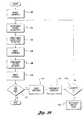
- FIG. 3a the method of detecting an open circuited load is depicted.
- the check for an open load is performed periodically whenever the MOSFET 36 is in the OFF state. Open circuits can also be checked when switching the MOSFET 36 from an ON to an OFF state.
- a counter is reset as indicated at block 78 and the I/O pin is configured as an output at block 80. After-configuring the I/O pin as an output, a low logic level is applied to the I/O pin at block 82.
- the MOSFET 36 If the MOSFET 36 is ON, this turns the MOSFET OFF and unlatches the predriver 10. If the MOSFET device is already off, applying a low logic level has no effect on the circuit. After a delay of 10 microseconds as indicated at block 84, the I/O pin is configured as an input at block 86 and after another 10 microsecond delay at block 88, the state of the I/O pin is read, to determined whether it is a logic level low or high, as indicated by the decision block 90. If the I/O pin remains low, no further action is required.
- the software for turning ON the power driver and detecting a short circuit in the load is depicted in the flowchart of Figure 3b.
- the counter is reset at 100 and the I/O pin is configured as an output at 102.
- a high logic level is applied to the I/O pin at 104 and after a delay of 100 milliseconds, indicated at 106, to permit the lamp 18 to heat up, to I/O pin is configured as an input at 108.
- the logic level on the I/O pin is read, to determined whether it is low or high, as indicated by the decision block 112. If the I/O pin remains high, no further action is taken.
- the counter is incremented at block 114, after a 500 millisecond delay to permit the MOSFET 38 to cool. If the counter is less than 3, as indicated by the decision block 118, the sequence is repeated by returning control to the block 102. After three consecutive detections of a short circuit condition, the short circuit flag is set at 120.
Landscapes
- Electronic Switches (AREA)
- Circuit Arrangement For Electric Light Sources In General (AREA)
- Emergency Protection Circuit Devices (AREA)
Claims (9)
- Schaltung zur Steuerung der Anlage einer Spannungsquelle (Vcc) an eine Last (18) und zur Überwachung des Zustandes der besagten Last (18), welche Schaltung (10) eine Treiberschaltung (16) zum Anschließen besagter Spannungsquelle an besagte Last (18) aufweist, wobei besagte Schaltung zwischen einem Anschlußpol (12) einer Steuervorrichtung (14) und besagter Last (18) angeschlossen ist, wobei besagte Steuervorrichtung (14) so ausgelegt ist, daß sie besagten Anschlußpol (12) als Eingabe- oder Ausgabepol konfiguriert, wobei besagte Schaltung (10) auf ein von besagter Steuervorrichtung (14) an besagten Anschlußpol (12) angelegtes Treiber-Steuerausgangssignal anspricht, wenn besagter Anschlußpol (12) als Ausgabepol konfiguriert ist, zur Verbindung einer Spannungsquelle mit besagter Last, wobei besagte Schaltung ein Eingabesignal für besagten Anschlußpol liefert, welches den Status der besagten Last (18) anzeigt, wenn besagter Anschlußpol (12) von besagter Steuervorrichtung (14) als Eingabepol konfiguriert ist;
dadurch gekennzeichnet, daß besagte Schaltung einen Pegelschalter (20) aufweist, welcher zwischen besagtem Anschlußpol und besagter Treiberschaltung (16) angeschlossen ist, eine Überwachungsschaltung (22), welche zwischen besagtem Anschlußpol (12) und einem Meßpunkt (24) zwischen besagter Treiberschaltung (16) und besagter Last (18) angeschlossen ist, zur Erfassung eines Zustandes der besagten Last und Abgabe des besagten Eingabesignals an besagte Steuervorrichtung (14), wobei besagtes Eingabesignal eine Rückkopplung zu besagtem Pegelschalter (20) bildet, so daß besagter Pegelschalter in Abwesenheit eines Fehlers an der Last in einem Zustand verriegelt wird, und so daß besagte Verriegelung deaktiviert und besagte Treiberschaltung (16) AUS-geschaltet wird, wenn ein Kurzschluß an besagter Last (18) vorliegt. - Schaltung nach Anspruch 1, worin besagte Schaltung besagten Treiber (16) in Reaktion auf einen Zustand des besagten Ausgabesignals in einem EIN-geschalteten Zustand verriegelt, wenn besagter Anschlußpol (12) als ein Ausgabepol konfiguriert ist, während kein Fehler an besagter Last vorliegt.
- Schaltung nach Anspruch 1 oder 2, worin besagter Treiber (16) eine MOSFET-Vorrichtung (36) enthält, wobei besagte Last im Source-Drain-Pfad der besagten MOSFET-Vorrichtung (36) liegt, wobei besagter Pegelschalter (20) ein Gate-Treibersignal an besagte MOSFET-Vorrichtung liefert, in Reaktion auf ein von besagter Steuervorrichtung (14) an besagtem Anschlußpol (12) angelegtes Signal mit einem ersten logischen Ausgangspegel, wobei besagte Überwachungsschaltung (22) derart auf die Source-Drain-Spannung der besagten MOSFET-Vorrichtung (36) anspricht, daß besagtes Signal mit dem ersten logischen Pegel an besagtem Anschlußpol (12) solange gehalten wird, wie besagte Source-Drain-Spannung unter einem vorgegebenen Spannungspegel liegt.
- Schaltung nach Anspruch 3, worin besagter vorgegebener Spannungspegel die VBE an einem Transistor (60) in besagter Überwachungsschaltung (22) ist.
- Schaltung nach Anspruch 4, worin besagte Last (18) zwischen besagtem Treiber (16) und einem Referenzpotential (Masse) angeschlossen ist.
- Schaltung nach Anspruch 5, worin besagte Steuervorrichtung (14) einen Mikroprozessor aufweist.
- Verfahren zur Steuerung und Überwachung des Zustandes eines Last-Schaltkreises (10) über einen einzigen Eingabe-/ Ausgabe-Pol (12) eines Mikroprozessors (14), wobei besagter Last-Schaltkreis eine Last (18) und Treibermittel (16) aufweist, welche mit besagtem Eingabe-/Ausgabe-Pol (12) verbunden sind, zur Bestromung der besagten Last (18), wobei besagtes Verfahren einen Ablauf der folgenden Schritte beinhaltet:dadurch gekennzeichnet, daß das Verfahren auf die Überwachung des Zustandes eines Last-Schaltkreises (10) angewendet wird, welcher einen zwischen dem Anschlußpol (12) und den Treibermitteln (16) angeschlossenen Pegelschalter (20) sowie eine Überwachungsschaltung (22) aufweist, die zwischen dem Anschlußpol (12) und einem Meßpunkt (24) zwischen den Treibermitteln (16) und der Last (18) zur Erfassung eines Zustandes der Last angeschlossen ist, wobei das Verfahren außerdem folgende Schritte aufweist:Konfigurieren des besagten Eingabe-/Ausgabe-Pols (12) als Ausgabe-Pol und Anlegen eines Signals mit einem hohen oder niedrigen logischen Pegel an besagten Eingabe-/Ausgabe-Pol, so daß besagte Treibermittel (16) veranlaßt werden, besagte Last (18) entweder in einen bestromten oder einen unbestromten Zustand zu versetzen,Konfigurieren des besagten Eingabe-/Ausgabe-Pols (12) als Eingabe-Pol und Überwachen des Spannungspegels an besagtem Anschlußpol,Speichern einer Last-Fehlerbedingung in Reaktion auf wenigstens eine Änderung des besagten Spannungspegels an besagtem Anschlußpol (12);Abgabe eines Rückkopplungssignals an besagten Pegelschalter (20) zur Verriegelung des besagten Pegelschalters in einem Zustand, wenn kein Last-Fehler vorliegt, undDeaktivierung der besagten Verriegelung und AUS-Schalten der besagten Treibermittel (16) in Reaktion auf einen Kurzschluß an besagter Last (18).
- Verfahren nach Anspruch 7, folgende weitere Schritte aufweisend:Abgabe eines hohen logischen Pegels von besagtem Mikroprozessor (14) an besagten Eingabe-/Ausgabe-Pol (12) zwecks Zulassung der Verriegelung des besagten Pegelschalters (20) zur Bestromung der besagten Last (18), undEntriegeln des besagten Pegelschalters (20) durch Abgabe eines Signals mit besagtem niedrigem logischem Pegel an besagten Eingabe-/Ausgabe-Pol (12), von der Überwachungsschaltung (22) aus, in Reaktion auf einen Kurzschluß an besagter Last (18).
- Verfahren nach Anspruch 7 oder 8, folgende weitere Schritte aufweisend:Abgabe eines niedrigen logischen Pegels an besagten Eingabe-/Ausgabe-Pol (12), von besagtem Mikroprozessor (14) aus, zur Deaktivierung der Verriegelung des besagten Pegelschalters, so daß besagte Last (18) deaktiviert wird, undAbgabe eines Signals mit besagtem hohem logischem Pegel von besagter Überwachungsschaltung (22) an besagten Eingabe-/Ausgabe-Pol (12) in Reaktion auf eine Stromkreisunterbrechung an besagter Last (18).
Applications Claiming Priority (2)
| Application Number | Priority Date | Filing Date | Title |
|---|---|---|---|
| US08/318,399 US5510950A (en) | 1994-10-05 | 1994-10-05 | Method and circuit for controlling and monitoring a load |
| US318399 | 1994-10-05 |
Publications (3)
| Publication Number | Publication Date |
|---|---|
| EP0709961A2 EP0709961A2 (de) | 1996-05-01 |
| EP0709961A3 EP0709961A3 (de) | 1997-11-05 |
| EP0709961B1 true EP0709961B1 (de) | 2001-02-21 |
Family
ID=23238035
Family Applications (1)
| Application Number | Title | Priority Date | Filing Date |
|---|---|---|---|
| EP19950307048 Expired - Lifetime EP0709961B1 (de) | 1994-10-05 | 1995-10-04 | Verfahren und Schaltung zur Steuerung und Überwachung einer Last |
Country Status (4)
| Country | Link |
|---|---|
| US (1) | US5510950A (de) |
| EP (1) | EP0709961B1 (de) |
| JP (1) | JPH08195661A (de) |
| DE (1) | DE69520130T2 (de) |
Families Citing this family (27)
| Publication number | Priority date | Publication date | Assignee | Title |
|---|---|---|---|---|
| JPH0894695A (ja) * | 1994-09-27 | 1996-04-12 | Mitsubishi Electric Corp | 半導体パワースイッチシステム |
| US5694282A (en) * | 1996-03-04 | 1997-12-02 | Ford Motor Company | Short circuit protection system |
| DE19705339C2 (de) * | 1997-02-12 | 2001-11-15 | Infineon Technologies Ag | Smart-Schalter sowie Verfahren zur Open-Load-Diagnose derselben |
| US6011416A (en) * | 1997-02-19 | 2000-01-04 | Harness System Technologies Research Ltd. | Switch circuit having excess-current detection function |
| US5920452A (en) | 1998-06-01 | 1999-07-06 | Harris Corporation | Circuit and method for protecting from overcurrent conditions and detecting an open electrical load |
| US6166893A (en) * | 1998-12-21 | 2000-12-26 | Semiconductor Components Industries, Llc | Semiconductor load driver circuit and method therefor |
| US6246559B1 (en) * | 1999-03-26 | 2001-06-12 | Honeywell International Inc | Power controller with short circuit protection |
| FR2796777B1 (fr) | 1999-07-20 | 2001-09-21 | St Microelectronics Sa | Commande d'un transistor mos de puissance |
| DE10025908A1 (de) * | 2000-05-26 | 2001-08-02 | Voith Turbo Kg | Leistungsschalter |
| CN1209877C (zh) | 2000-06-02 | 2005-07-06 | 汤姆森特许公司 | 产生电子迁移的装置和方法 |
| FI115426B (fi) * | 2000-12-22 | 2005-04-29 | Iws Int Oy | Kulkuneuvon sähkönjakelujärjestelmän älykäs sulakerasia |
| US7373561B2 (en) * | 2002-10-29 | 2008-05-13 | Broadcom Corporation | Integrated packet bit error rate tester for 10G SERDES |
| CN100373730C (zh) * | 2004-09-21 | 2008-03-05 | 深圳市珊星电脑有限公司 | 一种开关电源短路保护方法和电路 |
| US7256615B2 (en) * | 2005-01-31 | 2007-08-14 | Delphi Technologies, Inc. | Configurable high/low side driver using a low-side FET pre-driver |
| DE102005048801A1 (de) * | 2005-10-10 | 2007-04-12 | Conti Temic Microelectronic Gmbh | Schaltungsanordnung zur Beschaltung eines Ports eines Microprozessors |
| DE102005055832A1 (de) * | 2005-11-23 | 2007-05-24 | Patent-Treuhand-Gesellschaft für elektrische Glühlampen mbH | Schaltungsanordnung und Verfahren zum Ansteuern eines elektronischen Bauelements mit einem Ausgangssignal eines Mikroprozessors |
| US7583037B2 (en) | 2006-06-23 | 2009-09-01 | Spacesaver Corporation | Mobile storage unit with holding brake and single status line for load and drive detection |
| US7743616B2 (en) * | 2006-10-12 | 2010-06-29 | Thermo King Corporation | Control system for a generator |
| US7679370B2 (en) * | 2007-02-09 | 2010-03-16 | Delphi Technologies, Inc. | Controller having discrete driver circuitry connected to a single processor port |
| JP5044448B2 (ja) * | 2008-03-03 | 2012-10-10 | ルネサスエレクトロニクス株式会社 | 電源スイッチ回路 |
| CN102223506B (zh) * | 2011-05-25 | 2012-12-05 | 深圳创维-Rgb电子有限公司 | 一种电压跌落处理电路及电视机 |
| US9035642B2 (en) | 2011-06-30 | 2015-05-19 | Semiconductor Components Industries, Llc | Circuits for detecting AC- or DC-coupled loads |
| CN111542469B (zh) | 2017-08-01 | 2021-12-14 | 康明斯有限公司 | 将多个高侧负载与公共回位引脚相连接的控制逻辑电路 |
| WO2020139787A1 (en) * | 2018-12-28 | 2020-07-02 | Continental Automotive Systems, Inc. | Input voltage limiter for a microcontroller |
| CN111799759A (zh) * | 2020-07-23 | 2020-10-20 | 深圳市豪恩汽车电子装备股份有限公司 | 车载ecu输出电源的过流保护电路及其控制方法 |
| US11303275B2 (en) | 2020-09-03 | 2022-04-12 | Rockwell Automation Technologies, Inc. | Relay circuitry with self regulating charging |
| CN117239702A (zh) * | 2023-09-11 | 2023-12-15 | 宁波信泰机械有限公司 | 一种钳位限压电路 |
Family Cites Families (10)
| Publication number | Priority date | Publication date | Assignee | Title |
|---|---|---|---|---|
| DE3332386A1 (de) * | 1983-09-08 | 1985-03-21 | Vdo Adolf Schindling Ag, 6000 Frankfurt | Elektrische pruefeinrichtung eines fahrzeug-kombinationsinstruments |
| DE3338764A1 (de) * | 1983-10-26 | 1985-05-09 | Robert Bosch Gmbh, 7000 Stuttgart | Schaltungsanordnung zum ein- und ausschalten und ueberwachen elektrischer verbraucher |
| US4612638A (en) * | 1984-04-09 | 1986-09-16 | Chrysler Corporation | Diagnostic protection circuit and method using tri-state control and positive feedback |
| JPS61219216A (ja) * | 1985-03-25 | 1986-09-29 | Hitachi Ltd | 半導体スイツチ回路 |
| JPS61261643A (ja) * | 1985-05-14 | 1986-11-19 | Suzuki Motor Co Ltd | 車両用制御装置の故障検出装置 |
| JP2671132B2 (ja) * | 1988-06-24 | 1997-10-29 | 富士通テン株式会社 | パワードライバic |
| JP2542618Y2 (ja) * | 1988-08-30 | 1997-07-30 | アルプス電気株式会社 | 車載用負荷状態検知駆動装置 |
| JPH02179551A (ja) * | 1988-12-29 | 1990-07-12 | Nissan Motor Co Ltd | 車両用ランプ断線警報装置 |
| JP3028371B2 (ja) * | 1989-08-22 | 2000-04-04 | ヴアブコ・ヴエステイングハウス・フアールツオイクブレムゼン・ゲゼルシヤフト・ミツト・ベシユレンクテル・ハフツング | パワートランジスタ及びこれにより制御される負荷の監視方法 |
| DE4344013C1 (de) * | 1993-12-23 | 1995-03-23 | Kostal Leopold Gmbh & Co Kg | Elektrische Schaltungsanordnung |
-
1994
- 1994-10-05 US US08/318,399 patent/US5510950A/en not_active Expired - Fee Related
-
1995
- 1995-10-04 EP EP19950307048 patent/EP0709961B1/de not_active Expired - Lifetime
- 1995-10-04 DE DE69520130T patent/DE69520130T2/de not_active Expired - Fee Related
- 1995-10-04 JP JP25779495A patent/JPH08195661A/ja active Pending
Also Published As
| Publication number | Publication date |
|---|---|
| US5510950A (en) | 1996-04-23 |
| DE69520130D1 (de) | 2001-03-29 |
| JPH08195661A (ja) | 1996-07-30 |
| EP0709961A3 (de) | 1997-11-05 |
| EP0709961A2 (de) | 1996-05-01 |
| DE69520130T2 (de) | 2001-06-07 |
Similar Documents
| Publication | Publication Date | Title |
|---|---|---|
| EP0709961B1 (de) | Verfahren und Schaltung zur Steuerung und Überwachung einer Last | |
| US5920452A (en) | Circuit and method for protecting from overcurrent conditions and detecting an open electrical load | |
| JP3633522B2 (ja) | 負荷駆動回路 | |
| JP3427436B2 (ja) | 駆動回路 | |
| EP0426103B1 (de) | Elektronische Schutzanordnung für elektronische Schaltungen gegen unerwünschte Unterbrechung des Erdungsanschlusses | |
| US5852538A (en) | Power element driving circuit | |
| EP0602708B1 (de) | Steuerelektroden-Abschaltkreis für einen Leistungstransistor | |
| KR0177539B1 (ko) | 반도체 집적회로 | |
| US6472910B2 (en) | Electrical load driving device | |
| US5138516A (en) | Fault sensing and driving system for output driver device | |
| US4665459A (en) | Method and circuit for dissipating stored inductive energy | |
| US5192873A (en) | Fail-operational control system for vehicle loads | |
| US5923210A (en) | High side driver circuit with diagnostic output | |
| KR20010041222A (ko) | 전자 제어 유닛을 위한 전원 공급장치 | |
| US20040136129A1 (en) | Electric parts drive circuit | |
| US5424897A (en) | Three leaded protected power device having voltage input | |
| US5847911A (en) | Self-protecting switch apparatus for controlling a heat element of a vehicle seat and a method for providing the apparatus | |
| GB2236919A (en) | Overload and short-circuit protection of electric output drivers | |
| US5625518A (en) | Clamping circuit with reverse polarity protection | |
| US20020027391A1 (en) | Reduced current and power consumption structure of drive circuit | |
| EP0485119A2 (de) | Schaltung zum Ansteuern einer Last und zum Erzeugen eines Signales, das den Lastzustand anzeigt | |
| US5757601A (en) | Short circuit protection for high side driver | |
| JPH0317923A (ja) | 駆動回路の診断方式 | |
| CA2033951A1 (en) | Microcontroller controlled static input protection | |
| US5398148A (en) | Protection circuit for high side drivers |
Legal Events
| Date | Code | Title | Description |
|---|---|---|---|
| PUAI | Public reference made under article 153(3) epc to a published international application that has entered the european phase |
Free format text: ORIGINAL CODE: 0009012 |
|
| AK | Designated contracting states |
Kind code of ref document: A2 Designated state(s): DE FR GB |
|
| PUAL | Search report despatched |
Free format text: ORIGINAL CODE: 0009013 |
|
| AK | Designated contracting states |
Kind code of ref document: A3 Designated state(s): DE FR GB |
|
| 17P | Request for examination filed |
Effective date: 19980227 |
|
| 17Q | First examination report despatched |
Effective date: 19990712 |
|
| GRAG | Despatch of communication of intention to grant |
Free format text: ORIGINAL CODE: EPIDOS AGRA |
|
| GRAG | Despatch of communication of intention to grant |
Free format text: ORIGINAL CODE: EPIDOS AGRA |
|
| GRAH | Despatch of communication of intention to grant a patent |
Free format text: ORIGINAL CODE: EPIDOS IGRA |
|
| GRAH | Despatch of communication of intention to grant a patent |
Free format text: ORIGINAL CODE: EPIDOS IGRA |
|
| GRAA | (expected) grant |
Free format text: ORIGINAL CODE: 0009210 |
|
| AK | Designated contracting states |
Kind code of ref document: B1 Designated state(s): DE FR GB |
|
| REF | Corresponds to: |
Ref document number: 69520130 Country of ref document: DE Date of ref document: 20010329 |
|
| ET | Fr: translation filed | ||
| PGFP | Annual fee paid to national office [announced via postgrant information from national office to epo] |
Ref country code: GB Payment date: 20010914 Year of fee payment: 7 |
|
| PGFP | Annual fee paid to national office [announced via postgrant information from national office to epo] |
Ref country code: DE Payment date: 20011005 Year of fee payment: 7 |
|
| PGFP | Annual fee paid to national office [announced via postgrant information from national office to epo] |
Ref country code: FR Payment date: 20011011 Year of fee payment: 7 |
|
| PLBE | No opposition filed within time limit |
Free format text: ORIGINAL CODE: 0009261 |
|
| STAA | Information on the status of an ep patent application or granted ep patent |
Free format text: STATUS: NO OPPOSITION FILED WITHIN TIME LIMIT |
|
| REG | Reference to a national code |
Ref country code: GB Ref legal event code: IF02 |
|
| 26N | No opposition filed | ||
| PG25 | Lapsed in a contracting state [announced via postgrant information from national office to epo] |
Ref country code: GB Free format text: LAPSE BECAUSE OF NON-PAYMENT OF DUE FEES Effective date: 20021004 |
|
| PG25 | Lapsed in a contracting state [announced via postgrant information from national office to epo] |
Ref country code: DE Free format text: LAPSE BECAUSE OF NON-PAYMENT OF DUE FEES Effective date: 20030501 |
|
| GBPC | Gb: european patent ceased through non-payment of renewal fee |
Effective date: 20021004 |
|
| PG25 | Lapsed in a contracting state [announced via postgrant information from national office to epo] |
Ref country code: FR Free format text: LAPSE BECAUSE OF NON-PAYMENT OF DUE FEES Effective date: 20030630 |
|
| REG | Reference to a national code |
Ref country code: FR Ref legal event code: ST |