EP0715292A2 - Circuit de commande de plasma capable de supprimer la montée de courant dans les canaux à plasma d'un affichage - Google Patents
Circuit de commande de plasma capable de supprimer la montée de courant dans les canaux à plasma d'un affichage Download PDFInfo
- Publication number
- EP0715292A2 EP0715292A2 EP95118990A EP95118990A EP0715292A2 EP 0715292 A2 EP0715292 A2 EP 0715292A2 EP 95118990 A EP95118990 A EP 95118990A EP 95118990 A EP95118990 A EP 95118990A EP 0715292 A2 EP0715292 A2 EP 0715292A2
- Authority
- EP
- European Patent Office
- Prior art keywords
- discharge
- discharge channels
- current
- display device
- control means
- Prior art date
- Legal status (The legal status is an assumption and is not a legal conclusion. Google has not performed a legal analysis and makes no representation as to the accuracy of the status listed.)
- Ceased
Links
Images


Classifications
-
- G—PHYSICS
- G09—EDUCATION; CRYPTOGRAPHY; DISPLAY; ADVERTISING; SEALS
- G09G—ARRANGEMENTS OR CIRCUITS FOR CONTROL OF INDICATING DEVICES USING STATIC MEANS TO PRESENT VARIABLE INFORMATION
- G09G3/00—Control arrangements or circuits, of interest only in connection with visual indicators other than cathode-ray tubes
- G09G3/20—Control arrangements or circuits, of interest only in connection with visual indicators other than cathode-ray tubes for presentation of an assembly of a number of characters, e.g. a page, by composing the assembly by combination of individual elements arranged in a matrix no fixed position being assigned to or needed to be assigned to the individual characters or partial characters
- G09G3/34—Control arrangements or circuits, of interest only in connection with visual indicators other than cathode-ray tubes for presentation of an assembly of a number of characters, e.g. a page, by composing the assembly by combination of individual elements arranged in a matrix no fixed position being assigned to or needed to be assigned to the individual characters or partial characters by control of light from an independent source
- G09G3/36—Control arrangements or circuits, of interest only in connection with visual indicators other than cathode-ray tubes for presentation of an assembly of a number of characters, e.g. a page, by composing the assembly by combination of individual elements arranged in a matrix no fixed position being assigned to or needed to be assigned to the individual characters or partial characters by control of light from an independent source using liquid crystals
- G09G3/3611—Control of matrices with row and column drivers
- G09G3/3648—Control of matrices with row and column drivers using an active matrix
- G09G3/3662—Control of matrices with row and column drivers using an active matrix using plasma-addressed liquid crystal displays
-
- G—PHYSICS
- G09—EDUCATION; CRYPTOGRAPHY; DISPLAY; ADVERTISING; SEALS
- G09G—ARRANGEMENTS OR CIRCUITS FOR CONTROL OF INDICATING DEVICES USING STATIC MEANS TO PRESENT VARIABLE INFORMATION
- G09G2310/00—Command of the display device
- G09G2310/02—Addressing, scanning or driving the display screen or processing steps related thereto
- G09G2310/0264—Details of driving circuits
- G09G2310/0267—Details of drivers for scan electrodes, other than drivers for liquid crystal, plasma or OLED displays
-
- G—PHYSICS
- G09—EDUCATION; CRYPTOGRAPHY; DISPLAY; ADVERTISING; SEALS
- G09G—ARRANGEMENTS OR CIRCUITS FOR CONTROL OF INDICATING DEVICES USING STATIC MEANS TO PRESENT VARIABLE INFORMATION
- G09G2320/00—Control of display operating conditions
- G09G2320/04—Maintaining the quality of display appearance
- G09G2320/043—Preventing or counteracting the effects of ageing
Definitions
- the present invention generally relates to a plasma driver circuit for sequentially and selectively discharge-driving a plurality of discharge channels provided in plasma addressed display elements. More particularly, the present invention is directed to a technique for suppressing surge current flowing into the each channel when plasma discharging operations are commenced.
- Fig. 1 schematically represents a structure of the disclosed plasma addressed display element.
- the plasma addressed display element of this drawing owns such a flat panel structure that a display cell 101 and a plasma cell 102 are overlapped with each other via an intermediate substrate 103 made of a thin plate glass and the like.
- the plasma cell 102 is formed by employing a lower substrate 104, and a plurality of grooves 105 located in parallel to each other are provided on a surface of this lower substrate 104.
- Each of the grooves 105 is hermetically sealed by the intermediate substrate 103.
- Ionizable gas is filled into the grooves, and then discharge channels 106 are independently fabricated.
- Stripe-shaped protruded portions 107 existing between the successive grooves 105 have one function as an isolation wall for isolating the respective discharge channels 106, and have another function as a gap spacer of the lower substrate 104 with respect to the intermediate substrate 103.
- One pair of electrodes 108 and 109 are provided at a bottom of each groove 105, and arranged in parallel to each other.
- the electrodes pair may function as an anode electrode and a cathode electrode, which cause the gas filled in the discharge channel 106 to be ionized so as to produce plasma discharge therefrom.
- the display cell 101 is equipped with a liquid crystal 111 sandwiched by the intermediate substrate 103 and an upper substrate 110.
- a stripe-shaped signal electrode 112 is formed on an inner surface of the upper substrate 110. This signal electrode 112 is positioned perpendicular to the above-described discharge channel 106.
- the signal electrodes 112 are driven in unit of column, whereas the discharge channels 106 are driven in unit of row, so that matrix-shaped pixels are defined at intersecting (cross) portions of both the signal electrodes 112 and the discharge channels 106.
- one pair of a plasma driver circuit and a display driver circuit is used.
- the plasma driver circuit selectively scans the discharge channels 106 in the line sequential manner to produce plasma discharge, whereas the display driver circuit applies an image signal to the signal electrodes 112 in synchronism with the above-described line sequential scanning operation, thereby displaying a desired image.
- the inside thereof is maintained substantially at the anode potential. Under this condition, when the image signal is applied to the signal electrode 112, the image signal is written via the intermediate substrate 103 to the liquid crystal 111 of each pixel.
- the potential of the discharge channel 106 become a floating potential, so that the written image signal is held at each pixel.
- the discharge channel 106 functions as a sampling switch, while the liquid crystal 111 functions as a sampling capacitor.
- transmittance of the liquid crystal is varied and then the plasma addressed display elements are turned ON and OFF in unit of pixel.
- Fig. 2 is a circuit diagram for indicating one example of the conventional plasma driver circuit.
- V denotes a power supply voltage used to discharge a plasma display element
- Rr shows a resistor for limiting a discharge current flowing through a discharge channel.
- A denotes an anode electrode
- K represents a cathode electrode.
- a single discharge channel is constructed of one pair of these anode electrode and cathode electrode.
- symbol “Rp” represents a pull-up resistor used to hold the potential of the cathode electrode K at the anode potential during the non-selective state.
- This plasma driver circuit sequentially turns ON and OFF the switches SW1, SW2, ---, SWN to produce plasma discharge in each discharge channel.
- the image signal is supplied to the signal electrode, and the image signal is written into the pixel corresponding to the selected discharge channel.
- the power supply voltage V must be set to such a sufficiently large value defined on the basis of aging variations of plasma cells and also fluctuations in the discharge voltages of these discharge channels.
- the higher voltage than the required voltage is applied to the discharge channel whose discharge voltage is low, so that a large surge current may flow therethrough, resulting in damages of the cathode electrode and the anode electrode.
- lifetime of the plasma cells would be shortened.
- a driver circuit for a display device is comprised of: a plurality of discharge channels having a plurality of discharge electrodes; a plurality of switching means for sequentially selecting the discharge channels, the switching means being provided in one-to-one correspondence with each of the discharge channels; a current supplying means for supplying a drive current to the discharge channels through the switching means corresponding to each of the discharge channels; and a control means for controlling the current supplying means in synchronization with a switching timing of the switching means, the drive current being intermittently supplied to the discharge channels by the control means.
- a plurality of switches are sequentially turned ON/OFF so as to select the respective discharge channels.
- the pulse-form drive current is supplied to the selected discharge channel.
- the control circuit controls the pulse current waveform, so that the discharging drive voltages suitable for the respective discharge channels are applied to the relevant discharge channels.
- Fig. 4 is a circuit diagram of a plasma driver circuit according to an embodiment of the present invention.
- this plasma driver circuit is to sequentially and selectively drive a plurality of discharge channels 1 provided in plasma addressed display elements.
- Each of these discharge channels is constructed of one pair of an anode electrode "A” and a cathode electrode "K".
- a plurality of switches SW1, SW2, ---, SWN are employed correspondence to the respective discharge channels 1. These plural switches are sequentially turned ON/OFF to thereby select the respective discharge channels 1.
- a current source 2 is commonly connected via the switches SW1, SW2, ---, SWN to the cathode electrodes K of the respective discharge channels 1 so as to supply a predetermined drive current 2 thereto.
- this current source 2 is constructed by employing a field-effect transistor (FET) whose drain is connected to a common node "P".
- FET field-effect transistor
- this control circuit 3 controls the current source 2 to intermittently output a drive current I.
- This control circuit 3 further controls the waveform of this drive current I to apply voltages suitable for driving the respective discharge channels 1.
- the control circuit 3 is arranged with a sensing element 4 for producing a sensing signal corresponding to the drive current I, a signal source 5 for producing a waveform signal corresponding to the switching operation of the switch SW, and a differential amplifier 6 for controlling the current output of the current source 2 in accordance with a difference between the sensing signal and the waveform signal.
- the sensing element 4 is comprised of a sensing resistor Rd connected to the source of the FET which constitutes the current source 2.
- the signal source 5 is arranged with a signal generator (Sig Gen) for generating a rectangular pulse waveform signal.
- the differential amplifier 6 is arranged with an operational amplifier (OP Amp).
- the negative input terminal of this operational amplifier has the above-explained sensing signal applied thereto the positive input terminal has the waveform signal applied thereto, and the output terminal is connected to the gate electrode of the FET.
- symbol “V” shown in the circuit of Fig. 1 designates a power supply voltage to be applied to the plasma cell and the plasma drive circuit
- symbol “Rp” represents a pull-up resistor used to maintain the potential of the cathode electrode K at the anode potential during the non-selective state.
- signal “Cs” represents an equivalent internal capacitance of a plasma cell
- symbol “Rj” denotes a bias resistor.
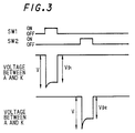
- the switches SW1, SW2, ---, SWN are sequentially turned ON/OFF.
- the current source 2 intermittently outputs the pulse-form drive current I.
- the control circuit 3 controls the current waveform so as to form a rectangular pulse shape.
- the control circuit 3 controls the height of this pulse-shaped current wave to be set to "Ip".
- control circuit 3 controls the drive current I after the rising operation of the respective discharge channels 1, so that the required discharge voltages are maintained.
- the control circuit 3 includes the sensing element 4, the signal source 5, and the differential amplifier 6 for maintaining the drive current to have a described waveform by the feedback control.
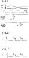
- Fig. 6 is a waveform chart for showing another example of the drive current I.
- This current waveform may be freely set by the signal with the waveform outputted from the signal source 5 shown in Fig. 4.
- the current waveform is set stepwise corresponding to operations when the discharge cell starts to be driven and when the discharge cell is continuously driven.
- a relatively large current Is may flow when the discharge cell stars to be driven, so that the internal capacitance Cs of the plasma cell is quickly charged.
- the voltage between A and K quickly reaches the required discharge voltage Vp. Thereafter, this relatively large current is changed into a relatively small current Ip when the discharge drive operation is maintained, so that the discharge state may be maintained.
- Fig. 7 is a waveform chart for indicating a further another example of the drive current I.
- This current waveform is basically similar to the current waveform shown in Fig. 6. In this case, however, a constant bias current Ij may be supplied even during the non-selective state.
- the potential at the common node P is increased up to the anode potential by the effect of the pull-up resistor Rp. Thereafter, to commence the next discharge operation, the internal capacitance Cs is again charged and then the potential at the common node P must be decreased.
- the internal capacitance Cs of the plasma cell must be repeatedly charged and discharged.
- a constant bias current Ij is supplied during the non-selective condition in order to maintain the potential of the common node P at the intermediate level.
- This intermediate level is set by providing the bias resistor Rj. For example, if this intermediate level is set to a level approximately equal to the extinction voltage, then the excessive charge/discharge operations of the internal capacitance Cs are no longer needed to be repeated.
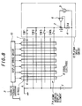
- Fig. 8 is a schematic block diagram for representing an overall driver circuit arrangement of a plasma addressed display element.
- the plasma addressed display element 7 owns the panel structure shown in Fig. 1, and is constructed of a display cell and a plasma cell.
- the display cell is equipped with a column-shaped signal electrode 8, whereas the plasma cell is equipped with a row-shaped discharge channel 1.
- a single discharge channel 1 is constructed of one pair of an anode electrode A and a cathode electrode K.
- a pixel 9 is defined at an intersecting portion between the signal electrode 8 and the discharge channel 1.
- a display drive circuit (column resistor) 10 is connected to each of the signal electrodes 8.
- a video data supply source 11 is connected to this display drive circuit 10. Meanwhile, a plasma drive circuit 12 is connected to each of the discharge channels 1.
- This plasma drive circuit 12 owns such a composition as shown in Fig. 4.
- An image signal for each horizontal line portion is transferred from the video data supply source 11 to the display drive circuit (column resistor) 10, and then is supplied to the signal electrodes 8.
- the plasma discharge is produced for each line, and the discharge channels 1 are line-sequentially brought into the selective condition.
- the image signal is written into the pixel 9 positioned on the selected line.
- this selected line is brought into the non-selective condition with the written image signal being maintained until the subsequent selective condition.
- the plasma drive circuit 12 sequentially supplies proper drive currents to each discharge channels 1 by way of the switches SW1, SW2, ---, SWN, the current source 2, and the control circuit (4, 5, 6) and so on.
- the plasma drive circuit is changed from the conventional switch system into the analog current control system.
- the applied voltage between the anode electrode and the cathode electrode is merely increased up to the discharge voltage of the relevant discharge channel irrespective of the external power supply voltage, the unnecessary surge current can be suppressed. Therefore, no damage is given to the anode electrode or the cathode electrode, and also the stable discharge operation can be maintained for a long time period. Since no compensation of the variations among the lines or the aged deteriorations in characteristics of the discharge channels is necessary, the power supply voltage can be easily set compared with the prior art.
Landscapes
- Engineering & Computer Science (AREA)
- Physics & Mathematics (AREA)
- Plasma & Fusion (AREA)
- Chemical & Material Sciences (AREA)
- Crystallography & Structural Chemistry (AREA)
- Computer Hardware Design (AREA)
- General Physics & Mathematics (AREA)
- Theoretical Computer Science (AREA)
- Control Of Indicators Other Than Cathode Ray Tubes (AREA)
- Liquid Crystal (AREA)
- Liquid Crystal Display Device Control (AREA)
Applications Claiming Priority (2)
| Application Number | Priority Date | Filing Date | Title |
|---|---|---|---|
| JP6329448A JPH08160908A (ja) | 1994-12-02 | 1994-12-02 | プラズマ駆動回路 |
| JP329448/94 | 1994-12-02 |
Publications (2)
| Publication Number | Publication Date |
|---|---|
| EP0715292A2 true EP0715292A2 (fr) | 1996-06-05 |
| EP0715292A3 EP0715292A3 (fr) | 1996-09-04 |
Family
ID=18221493
Family Applications (1)
| Application Number | Title | Priority Date | Filing Date |
|---|---|---|---|
| EP95118990A Ceased EP0715292A3 (fr) | 1994-12-02 | 1995-12-01 | Circuit de commande de plasma capable de supprimer la montée de courant dans les canaux à plasma d'un affichage |
Country Status (6)
| Country | Link |
|---|---|
| US (1) | US5696522A (fr) |
| EP (1) | EP0715292A3 (fr) |
| JP (1) | JPH08160908A (fr) |
| KR (1) | KR960025299A (fr) |
| CN (1) | CN1132894A (fr) |
| TW (1) | TW409234B (fr) |
Cited By (1)
| Publication number | Priority date | Publication date | Assignee | Title |
|---|---|---|---|---|
| EP0784306A1 (fr) * | 1996-01-12 | 1997-07-16 | Sony Corporation | Dispositif d'affichage adressé par plasma |
Families Citing this family (13)
| Publication number | Priority date | Publication date | Assignee | Title |
|---|---|---|---|---|
| JP3395399B2 (ja) * | 1994-09-09 | 2003-04-14 | ソニー株式会社 | プラズマ駆動回路 |
| JP2900997B2 (ja) * | 1996-11-06 | 1999-06-02 | 富士通株式会社 | 表示ユニットの消費電力制御のための方法と装置、それを備えた表示システム及びそれを実現するプログラムを格納した記憶媒体 |
| JP3568098B2 (ja) * | 1998-06-03 | 2004-09-22 | パイオニア株式会社 | 表示パネルの駆動装置 |
| JP3549441B2 (ja) * | 1998-06-22 | 2004-08-04 | シャープ株式会社 | 定電流制御装置 |
| JP3556097B2 (ja) | 1998-06-30 | 2004-08-18 | 富士通株式会社 | プラズマディスプレイパネル駆動方法 |
| KR100450218B1 (ko) * | 2001-10-16 | 2004-09-24 | 삼성에스디아이 주식회사 | 플라즈마 디스플레이 패널의 구동 장치 및 그 구동 방법 |
| JP4095784B2 (ja) * | 2001-10-19 | 2008-06-04 | 富士通日立プラズマディスプレイ株式会社 | プラズマディスプレイ装置 |
| KR100448190B1 (ko) * | 2002-01-21 | 2004-09-10 | 삼성전자주식회사 | 플라즈마 디스플레이패널장치 |
| TWI260509B (en) * | 2002-08-15 | 2006-08-21 | Sony Corp | Method and apparatus for processing image data and semiconductor storage device |
| US7668591B2 (en) * | 2003-09-18 | 2010-02-23 | Cardiac Pacemakers, Inc. | Automatic activation of medical processes |
| KR100570994B1 (ko) * | 2003-11-27 | 2006-04-13 | 삼성에스디아이 주식회사 | 디스플레이 전원제어장치 |
| CN108333453B (zh) * | 2018-03-20 | 2020-11-10 | 江苏邦士医疗科技有限公司 | 降低信号源内部冲击电流及等离子体产生的软件处理算法 |
| CN111225487A (zh) * | 2019-07-16 | 2020-06-02 | 中国人民解放军空军工程大学 | 一种单电源电弧等离子体阵列式布局的流动控制装置及控制方法 |
Citations (3)
| Publication number | Priority date | Publication date | Assignee | Title |
|---|---|---|---|---|
| EP0326254A2 (fr) * | 1988-01-19 | 1989-08-02 | Tektronix, Inc. | Appareil et méthode d'adressage d'éléments d'emmagasinage de données |
| US4896149A (en) | 1988-01-19 | 1990-01-23 | Tektronix, Inc. | Addressing structure using ionizable gaseous medium |
| US5077553A (en) | 1988-01-19 | 1991-12-31 | Tektronix, Inc. | Apparatus for and methods of addressing data storage elements |
Family Cites Families (9)
| Publication number | Priority date | Publication date | Assignee | Title |
|---|---|---|---|---|
| JPS5443762A (en) * | 1977-09-13 | 1979-04-06 | Seiko Epson Corp | Liquid crystal mechanism |
| US4250504A (en) * | 1979-08-23 | 1981-02-10 | General Electric Company | Gas discharge display circuit |
| DE3176916D1 (en) * | 1980-07-07 | 1988-11-24 | Interstate Electronics Corp | Plasma display panel drive |
| JPH01185692A (ja) * | 1988-01-19 | 1989-07-25 | Sanyo Electric Co Ltd | 平面ディスプレイパネル |
| JP2619027B2 (ja) * | 1988-11-30 | 1997-06-11 | シャープ株式会社 | 表示装置の駆動方法および装置 |
| US5008657A (en) * | 1989-01-31 | 1991-04-16 | Varo, Inc. | Self adjusting matrix display |
| US5111195A (en) * | 1989-01-31 | 1992-05-05 | Sharp Kabushiki Kaisha | Driving circuit for a matrix type display device |
| JP3326815B2 (ja) * | 1992-04-24 | 2002-09-24 | ソニー株式会社 | プラズマアドレス電気光学装置 |
| TW247358B (fr) * | 1993-03-04 | 1995-05-11 | Tektronix Inc |
-
1994
- 1994-12-02 JP JP6329448A patent/JPH08160908A/ja active Pending
-
1995
- 1995-11-30 TW TW084112772A patent/TW409234B/zh not_active IP Right Cessation
- 1995-12-01 KR KR1019950045998A patent/KR960025299A/ko not_active Withdrawn
- 1995-12-01 CN CN95120031A patent/CN1132894A/zh active Pending
- 1995-12-01 EP EP95118990A patent/EP0715292A3/fr not_active Ceased
- 1995-12-01 US US08/565,896 patent/US5696522A/en not_active Expired - Fee Related
Patent Citations (3)
| Publication number | Priority date | Publication date | Assignee | Title |
|---|---|---|---|---|
| EP0326254A2 (fr) * | 1988-01-19 | 1989-08-02 | Tektronix, Inc. | Appareil et méthode d'adressage d'éléments d'emmagasinage de données |
| US4896149A (en) | 1988-01-19 | 1990-01-23 | Tektronix, Inc. | Addressing structure using ionizable gaseous medium |
| US5077553A (en) | 1988-01-19 | 1991-12-31 | Tektronix, Inc. | Apparatus for and methods of addressing data storage elements |
Cited By (2)
| Publication number | Priority date | Publication date | Assignee | Title |
|---|---|---|---|---|
| EP0784306A1 (fr) * | 1996-01-12 | 1997-07-16 | Sony Corporation | Dispositif d'affichage adressé par plasma |
| US5889502A (en) * | 1996-01-12 | 1999-03-30 | Sony Corporation | Discharge voltage control for plasma addressed display device |
Also Published As
| Publication number | Publication date |
|---|---|
| TW409234B (en) | 2000-10-21 |
| US5696522A (en) | 1997-12-09 |
| KR960025299A (ko) | 1996-07-20 |
| EP0715292A3 (fr) | 1996-09-04 |
| CN1132894A (zh) | 1996-10-09 |
| JPH08160908A (ja) | 1996-06-21 |
Similar Documents
| Publication | Publication Date | Title |
|---|---|---|
| US5696522A (en) | Plasma driver circuit capable of surpressing surge current of plasma display channel | |
| EP0362948B1 (fr) | Dispositif d'affichage à matrice | |
| JP3863214B2 (ja) | ビデオ信号供給装置 | |
| JPH075852A (ja) | 液晶表示装置で漏話を除去する方法及び液晶表示装置 | |
| EP0567020B1 (fr) | Dispositif électro-optique adressé à plasma et méthode d'adressage correspondant | |
| US5909199A (en) | Plasma driving circuit | |
| US4779956A (en) | Driving circuit for liquid crystal display | |
| US5706020A (en) | Plasma addressed display | |
| JP3319042B2 (ja) | プラズマアドレス表示装置 | |
| US5889502A (en) | Discharge voltage control for plasma addressed display device | |
| US5657035A (en) | Plasma addressed liquid crystal display device operable under optimum line sequential drive timing | |
| US5760753A (en) | Method of driving plasma addressed display panel | |
| US6483488B1 (en) | Display apparatus and method of driving the display apparatus | |
| JPH08110513A (ja) | プラズマアドレス表示装置 | |
| US6081245A (en) | Plasma-addressed liquid crystal display device | |
| KR100531790B1 (ko) | 평판 디스플레이 패널 구동 방법 | |
| JPH07244268A (ja) | プラズマアドレス液晶表示装置 | |
| JPH09311320A (ja) | プラズマアドレス型液晶表示装置 | |
| JPH09200661A (ja) | プラズマアドレス表示装置 | |
| JPH08304768A (ja) | プラズマアドレス表示装置 | |
| JPH0772458A (ja) | プラズマアドレス液晶表示装置 | |
| KR20030057044A (ko) | 액정 패널의 잔상 제거장치 및 방법 | |
| JPH07295502A (ja) | プラズマアドレス表示装置 | |
| JPH06289808A (ja) | プラズマアドレス表示素子の駆動方法 | |
| JPH08304770A (ja) | プラズマアドレス表示装置 |
Legal Events
| Date | Code | Title | Description |
|---|---|---|---|
| PUAI | Public reference made under article 153(3) epc to a published international application that has entered the european phase |
Free format text: ORIGINAL CODE: 0009012 |
|
| AK | Designated contracting states |
Kind code of ref document: A2 Designated state(s): DE FR GB |
|
| PUAL | Search report despatched |
Free format text: ORIGINAL CODE: 0009013 |
|
| AK | Designated contracting states |
Kind code of ref document: A3 Designated state(s): DE FR GB |
|
| 17P | Request for examination filed |
Effective date: 19970204 |
|
| 17Q | First examination report despatched |
Effective date: 20000912 |
|
| GRAG | Despatch of communication of intention to grant |
Free format text: ORIGINAL CODE: EPIDOS AGRA |
|
| STAA | Information on the status of an ep patent application or granted ep patent |
Free format text: STATUS: THE APPLICATION HAS BEEN REFUSED |
|
| 18R | Application refused |
Effective date: 20020518 |