EP0715346A2 - Verfahren zur Herstellung eines MESFETS mit einer T-förmigen Gitterelektrode und dadurch hergestelltes Bauelement - Google Patents
Verfahren zur Herstellung eines MESFETS mit einer T-förmigen Gitterelektrode und dadurch hergestelltes Bauelement Download PDFInfo
- Publication number
- EP0715346A2 EP0715346A2 EP95306668A EP95306668A EP0715346A2 EP 0715346 A2 EP0715346 A2 EP 0715346A2 EP 95306668 A EP95306668 A EP 95306668A EP 95306668 A EP95306668 A EP 95306668A EP 0715346 A2 EP0715346 A2 EP 0715346A2
- Authority
- EP
- European Patent Office
- Prior art keywords
- insulating film
- forming
- gate electrode
- film
- semiconductor layer
- Prior art date
- Legal status (The legal status is an assumption and is not a legal conclusion. Google has not performed a legal analysis and makes no representation as to the accuracy of the status listed.)
- Granted
Links
Images



Classifications
-
- H—ELECTRICITY
- H10—SEMICONDUCTOR DEVICES; ELECTRIC SOLID-STATE DEVICES NOT OTHERWISE PROVIDED FOR
- H10D—INORGANIC ELECTRIC SEMICONDUCTOR DEVICES
- H10D30/00—Field-effect transistors [FET]
- H10D30/01—Manufacture or treatment
- H10D30/061—Manufacture or treatment of FETs having Schottky gates
- H10D30/0612—Manufacture or treatment of FETs having Schottky gates of lateral single-gate Schottky FETs
- H10D30/0614—Manufacture or treatment of FETs having Schottky gates of lateral single-gate Schottky FETs using processes wherein the final gate is made after the completion of the source and drain regions, e.g. gate-last processes using dummy gates
-
- H—ELECTRICITY
- H10—SEMICONDUCTOR DEVICES; ELECTRIC SOLID-STATE DEVICES NOT OTHERWISE PROVIDED FOR
- H10D—INORGANIC ELECTRIC SEMICONDUCTOR DEVICES
- H10D30/00—Field-effect transistors [FET]
- H10D30/40—FETs having zero-dimensional [0D], one-dimensional [1D] or two-dimensional [2D] charge carrier gas channels
- H10D30/47—FETs having zero-dimensional [0D], one-dimensional [1D] or two-dimensional [2D] charge carrier gas channels having two-dimensional [2D] charge carrier gas channels, e.g. nanoribbon FETs or high electron mobility transistors [HEMT]
- H10D30/471—High electron mobility transistors [HEMT] or high hole mobility transistors [HHMT]
- H10D30/475—High electron mobility transistors [HEMT] or high hole mobility transistors [HHMT] having wider bandgap layer formed on top of lower bandgap active layer, e.g. undoped barrier HEMTs such as i-AlGaN/GaN HEMTs
- H10D30/4755—High electron mobility transistors [HEMT] or high hole mobility transistors [HHMT] having wider bandgap layer formed on top of lower bandgap active layer, e.g. undoped barrier HEMTs such as i-AlGaN/GaN HEMTs having wide bandgap charge-carrier supplying layers, e.g. modulation doped HEMTs such as n-AlGaAs/GaAs HEMTs
-
- H—ELECTRICITY
- H10—SEMICONDUCTOR DEVICES; ELECTRIC SOLID-STATE DEVICES NOT OTHERWISE PROVIDED FOR
- H10D—INORGANIC ELECTRIC SEMICONDUCTOR DEVICES
- H10D30/00—Field-effect transistors [FET]
- H10D30/60—Insulated-gate field-effect transistors [IGFET]
- H10D30/67—Thin-film transistors [TFT]
- H10D30/6729—Thin-film transistors [TFT] characterised by the electrodes
- H10D30/6737—Thin-film transistors [TFT] characterised by the electrodes characterised by the electrode materials
- H10D30/6738—Schottky barrier electrodes
-
- H—ELECTRICITY
- H10—SEMICONDUCTOR DEVICES; ELECTRIC SOLID-STATE DEVICES NOT OTHERWISE PROVIDED FOR
- H10D—INORGANIC ELECTRIC SEMICONDUCTOR DEVICES
- H10D30/00—Field-effect transistors [FET]
- H10D30/60—Insulated-gate field-effect transistors [IGFET]
- H10D30/67—Thin-film transistors [TFT]
- H10D30/674—Thin-film transistors [TFT] characterised by the active materials
- H10D30/675—Group III-V materials, Group II-VI materials, Group IV-VI materials, selenium or tellurium
-
- H—ELECTRICITY
- H10—SEMICONDUCTOR DEVICES; ELECTRIC SOLID-STATE DEVICES NOT OTHERWISE PROVIDED FOR
- H10D—INORGANIC ELECTRIC SEMICONDUCTOR DEVICES
- H10D30/00—Field-effect transistors [FET]
- H10D30/80—FETs having rectifying junction gate electrodes
- H10D30/87—FETs having Schottky gate electrodes, e.g. metal-semiconductor FETs [MESFET]
-
- H—ELECTRICITY
- H10—SEMICONDUCTOR DEVICES; ELECTRIC SOLID-STATE DEVICES NOT OTHERWISE PROVIDED FOR
- H10D—INORGANIC ELECTRIC SEMICONDUCTOR DEVICES
- H10D64/00—Electrodes of devices having potential barriers
- H10D64/01—Manufacture or treatment
- H10D64/012—Manufacture or treatment of electrodes comprising a Schottky barrier to a semiconductor
- H10D64/0124—Manufacture or treatment of electrodes comprising a Schottky barrier to a semiconductor to Group III-V semiconductors
- H10D64/0125—Manufacture or treatment of electrodes comprising a Schottky barrier to a semiconductor to Group III-V semiconductors characterised by the sectional shape, e.g. T or inverted T
-
- H—ELECTRICITY
- H10—SEMICONDUCTOR DEVICES; ELECTRIC SOLID-STATE DEVICES NOT OTHERWISE PROVIDED FOR
- H10D—INORGANIC ELECTRIC SEMICONDUCTOR DEVICES
- H10D64/00—Electrodes of devices having potential barriers
- H10D64/20—Electrodes characterised by their shapes, relative sizes or dispositions
- H10D64/27—Electrodes not carrying the current to be rectified, amplified, oscillated or switched, e.g. gates
- H10D64/311—Gate electrodes for field-effect devices
- H10D64/411—Gate electrodes for field-effect devices for FETs
-
- H—ELECTRICITY
- H10—SEMICONDUCTOR DEVICES; ELECTRIC SOLID-STATE DEVICES NOT OTHERWISE PROVIDED FOR
- H10D—INORGANIC ELECTRIC SEMICONDUCTOR DEVICES
- H10D64/00—Electrodes of devices having potential barriers
- H10D64/60—Electrodes characterised by their materials
- H10D64/64—Electrodes comprising a Schottky barrier to a semiconductor
-
- H—ELECTRICITY
- H10—SEMICONDUCTOR DEVICES; ELECTRIC SOLID-STATE DEVICES NOT OTHERWISE PROVIDED FOR
- H10D—INORGANIC ELECTRIC SEMICONDUCTOR DEVICES
- H10D62/00—Semiconductor bodies, or regions thereof, of devices having potential barriers
- H10D62/80—Semiconductor bodies, or regions thereof, of devices having potential barriers characterised by the materials
- H10D62/85—Semiconductor bodies, or regions thereof, of devices having potential barriers characterised by the materials being Group III-V materials, e.g. GaAs
-
- Y—GENERAL TAGGING OF NEW TECHNOLOGICAL DEVELOPMENTS; GENERAL TAGGING OF CROSS-SECTIONAL TECHNOLOGIES SPANNING OVER SEVERAL SECTIONS OF THE IPC; TECHNICAL SUBJECTS COVERED BY FORMER USPC CROSS-REFERENCE ART COLLECTIONS [XRACs] AND DIGESTS
- Y10—TECHNICAL SUBJECTS COVERED BY FORMER USPC
- Y10S—TECHNICAL SUBJECTS COVERED BY FORMER USPC CROSS-REFERENCE ART COLLECTIONS [XRACs] AND DIGESTS
- Y10S148/00—Metal treatment
- Y10S148/10—Lift-off masking
-
- Y—GENERAL TAGGING OF NEW TECHNOLOGICAL DEVELOPMENTS; GENERAL TAGGING OF CROSS-SECTIONAL TECHNOLOGIES SPANNING OVER SEVERAL SECTIONS OF THE IPC; TECHNICAL SUBJECTS COVERED BY FORMER USPC CROSS-REFERENCE ART COLLECTIONS [XRACs] AND DIGESTS
- Y10—TECHNICAL SUBJECTS COVERED BY FORMER USPC
- Y10S—TECHNICAL SUBJECTS COVERED BY FORMER USPC CROSS-REFERENCE ART COLLECTIONS [XRACs] AND DIGESTS
- Y10S438/00—Semiconductor device manufacturing: process
- Y10S438/942—Masking
- Y10S438/948—Radiation resist
- Y10S438/951—Lift-off
Definitions
- the present invention relates to a semiconductor device and its production method and, more specifically, to a semiconductor device containing a compound semiconductor transistor having an electrode, such as a T-shaped gate electrode.
- a field effect transistor using a compound semiconductor is widely used as a micro wave device because of its superior high frequency characteristics.
- a GaAsMESFET, a HEMT and the like comprising a compound semiconductor into an MMIC (monolithic microwave IC), wherein stabilization of a threshold voltage of a transistor and control accuracy of the threshold voltage are important.
- the GaAsMESFET has an active semiconductor layer 102 containing some impurities which are formed over a semi-insulating compound semiconductor substrate 101, a gate electrode 103 which is formed on the active semiconductor layer 102, and a source electrode 106 and a drain electrode 107 which are formed on the active semiconductor layer 102 at each side of the gate electrode 103 through a contact layer 105.
- the gate electrode 103, the active semiconductor layer 102, the contact layer 105 and the like are covered with a protection layer 108 built using a material such as silicon oxide and silicon nitride.
- the gate electrode 103 and the active semiconductor layer 102 are respectively stressed and tend to generate electric polarization in the compound semiconductor layer, whereby polarized charge is developed across a semiconductor crystal to cause a piezoelectric effect. If the polarized charge occurs, a gate voltage threshold becomes unstable.
- Japanese Patent Laid-Open No. 95573/1986 describes that impurities are implanted into a gate electrode for controlling a stress from the gate electrode per se.
- Japanese Patent Laid-Open No. 20629/1989 and Japanese Patent Laid-Open No. 247618/1990 describe that a stress from a gate electrode is cancelled utilizing a stress from an insulating film which covers the gate electrode, by which the stress from the gate electrode can be controlled by changing a thickness of the insulating film.
- the stress from the gate electrode made only of tungsten silicide (WSi) can be controlled to some extent by changing sputtering conditions for WSi growth.
- Japanese Patent Laid-Open No. 282841/1992 describes that a stress is adjusted by covering a semi-conductor layer at a side of a gate electrode with an insulating film and then exposing the insulating film to oxygen plasma or nitrogen plasma.
- T-shaped gate electrode deviation of the threshold voltage caused by a piezoelectric effect is adjusted by covering a gate electrode having a square cross section which is formed by self-align techniques or lift-off techniques, however, these techniques described above cannot be applied as they are to the gate electrode which has a simplified T-shaped cross section (hereinafter referred to as a T-shaped gate electrode).
- the T-shaped gate electrode In the T-shaped gate electrode, its narrow bottom surface forms a Schottky contact with a substrate layer. This bottom surface is made small as the gate length is decreased.
- the upper side of the T-shaped gate electrode widely expands to form an overhang-like extension to the lower side thereof for lowering the resistance, and a low resistance layer made of the other material is often stacked thereon.
- the amount of stress cannot be stably controlled since the stresses applied to the upper and lower parts of the electrode are not uniform when a single insulating film is used and, as the result, controlling a threshold voltage becomes difficult.
- a first insulating film is selectively formed underneath an overhang of a gate electrode which is formed wider at the upper side, and side faces of the upper portion of the gate electrode, side faces of the first insulating film, and a surface of a compound semiconductor layer under the gate electrode are covered with a second insulating film for controlling the threshold voltage.
- the second insulating film equivalently covers the gate electrode having a square cross section, whereby stresses applied to a side area of the gate electrode are made uniform and controlling a threshold voltage is facilitated.
- the first insulating film forming area is largely extended from underneath the overhang of the gate electrode to both sides, then the stress from the second insulating film is not applied to the lower narrow area of the gate electrode, which makes controlling the threshold voltage difficult.
- the first insulating film is completely removed and subsequently the gate electrode which has an upper wide area is covered only with the second insulating film, then a cavity is produced under the overhang of the gate electrode and the stress from the second insulating film is not applied to the lower narrow area of the gate electrode, which makes controlling the threshold voltage difficult.
- the underneath of the overhang is filled with the second insulating film, then the stresses applied externally to the lower and upper parts of the T-shaped gate does not become uniform, accordingly, it is difficult to control the threshold voltage with the second insulating film.
- a single resist containing windows at a source region and a drain region is provided on the first insulating film.
- the first insulating film is left under the overhang of the gate electrode by isotropically etching the insulating film at both sides of the gate electrode to remove the insulating film in the source region and the drain region.
- a source electrode and a drain electrode are made on a compound semiconductor layer using a lift-off method wherein the resist is used as a mask.
- the resist is used not only as a mask for patterning the first insulating film but also as a mask for making a source electrode and a drain electrode, a mask-making process is simplified.
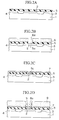
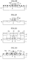
- Figs. 2A to 2H are cross-sectional views illustrating a manufacturing process of a GaAsMESFET associated with a first embodiment of the present invention.
- silicon is ion-implanted to an element forming region in a semi-insulating compound semiconductor substrate 1 made of GaAs, then silicon is implanted again to each side of the element forming region.
- the impurity (silicon) is activated by annealing, and an n-type impurity diffused region 2 and n + -type impurity diffused regions 3 and 4 on both sides thereof are formed.
- the n-type impurity diffused region 2 and the n + -type impurity diffused regions 3 and 4 constitute an active semiconductor layer and the n-type impurity diffused region 2 serves as a channel region.
- Requirements for implanting silicon ion to form the n-type impurity diffused region 2 are to meet the acceleration energy of 9.612 x 10 -15 J (60 keV) and the dose amount of 4 x 10 cm -2 .
- an insulating spacer layer 5 is formed on the compound semiconductor substrate 1 to a thickness of 300 nm.
- resist 6 is applied over the spacer layer 5, exposed to light, and developed to form a first window 6a for a gate 6 which runs through the approximate center of the n-type impurity diffused region 2.
- the window 6a for a gate may be displaced not at the center of the n-type impurity diffused region 2 but to the source region to improve a drain dielectric strength.
- the spacer layer 5 underneath the first window 6a for a gate is removed by reactive ion etching (RIE), whereby an opening 5a is formed underneath the first window 6a for a gate.
- RIE reactive ion etching
- a film for example, a tungsten silicide (WSi) film 7, to be in Schottky-junction with the compound semiconductor substrate 1, is formed on the spacer layer 5 and on the inside of the opening 5a to a thickness of 100 nm by sputtering.
- a second resist 8 is applied on the WSi film 7, exposed to light, and developed to form a second window 8a for a gate, which is larger than the opening 5a, over the opening 5a.
- gold is grown in the second window 8a for a gate to a thickness of 700 nm by electrolytic plating.
- the WSi film 7 As a corresponding area of the WSi film 7 where a gold layer 9 is not covered is removed by reactive ion etching (RIE) after removal of the second resist 8, the WSi film 7 obtains an simplified T-shaped cross section over which the T-shaped gold layer 9 is provided as shown in Fig. 2E. These WSi film 7 and gold layer 9 together constitute a T-shaped gate electrode 10. Subsequently, as shown in Fig. 2F, a corresponding area of the spacer layer 5 which is not covered with a gold layer 9 is removed by reactive ion etching to allow to leave it only underneath an overhang 10a of the gate electrode.
- RIE reactive ion etching
- SF 6 is used as an etching gas for the spacer layer 5
- a mixed gas of CF 4 and CHF 3 is used as a etching gas for a spacer layer 5.
- the T-shaped gate electrode 10 is hard to be decreased since the WSi film 7 is covered with the gold layer which is hard to react with the reactive etching such as the RIE.
- High sensitive resist 11 and low sensitive resist 12 are applied onto the compound semiconductor substrate 1 in sequence. Then the high sensitive resist 11 on the n + -type impurity diffused regions 3 and 4 is exposed to light with a low exposure amount. In turn, the low sensitive resist 12 is exposed to light with the exposed area being restricted narrower and the light exposure amount being increased. Next, the two-layer resist 11 and 12 is developed to form two windows 13a and 13b on the n + -type impurity diffused region 3 and 4. In this case, as the low sensitive resist 12 is not exposed to light with a low exposure amount, each of cross sections of these windows 13a and 13b is respectively formed like an overhang with the low sensitive resist 12 expanding.
- a metal film 14 of two-layer structure composed of gold germanium alloy (AuGe) and gold (Au) is formed by sputtering. Then, when the two-layer resist 11 and 12 is removed, the metal layer 14 is left only over two regions of n + impurity diffused layer 3, 4, so that one of these regions is used as a source electrode 14s and the other is used as a drain electrode 14d. Owing to the overhang-shaped resist 11 and 12, the metal film 14 can be provided near exactly. AuGe which constitutes the metal layer 14 provides an ohmic contact to the compound semiconductor substrate made of GaAs.
- Characteristics of the transistor formed on the compound semiconductor substrate as mentioned above are estimated and a threshold voltage thereof is measured. Then, as shown in Fig. 2H, the transistor is covered with an threshold control insulating film 15 made of silicon nitride. At this time, based on relationship between a film thickness of the threshold control insulating film 15 and the threshold voltage or relationship between a film thickness of the threshold control insulating film 15 and a source-drain current which have been obtained previously, a threshold voltage is adjusted to a desired value depending on the thickness of the threshold control insulating film 15.
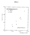
- a stress of silicon nitride used for the threshold control insulating film 15 one example of relationship between a threshold voltage change amount ⁇ th and a thickness of the threshold control insulating film 15 is shown in Fig. 3.
- a gate length L g indicates a length of a gate electrode in a channel length direction
- a gate width W g indicates a length of a gate electrode in a direction perpendicular to the gate length.
- the stress per unit area of the threshold control insulating film 15 is approximately constant independent of a film thickness, however, as the film thickness is increased, the stress applied to the gate electrode 10 will rise.
- a threshold control insulating film 15 and a gate length L g and a gate width W g are respectively 0.5 ⁇ m and 20 ⁇ m
- the product of the stress per unit area of the threshold control insulating film 15 and the film thickness thereof is 10 0 N/m is (1 x 10 5 dyn/cm) or more.
- nitride silicon provided with a stress per unit area is at least -6.2 x 10 6 N/m 2 (-6.2 x 10 9 dyn/cm 2) .
- the spacer layer 5 made of SiO 2 is patterned using the gate electrode 10 as a mask, the spacer layer 5 under overhangs at both sides of the gate electrode 10 will not extend beyond the gate electrode 10. Accordingly, since the stress of the threshold control insulating film 15 is applied to the lower part of the gate electrode 10 without so attenuated by the spacer layer 5, controlling the stress of the threshold control insulating film 15 is so facilitated.
- the threshold control insulating film 15 equivalently covers the gate electrode having a square cross section, the stress applied to the T-shaped gate electrode 10 is uniform and adjustment of the threshold voltage is facilitated.
- the stress of the spacer layer 5 becomes the dominant force as a stress applied to the lower part of the gate electrode 10 from the threshold control insulating film 15 and the adjustment of the threshold voltage using the stress of the threshold control insulating film 15 becomes difficult. That is, the stress of the threshold control insulating film 15 is not applied to the lower part of the gate electrode through the spacer layer 5.
- the threshold voltage adjustment becomes impossible because the stress from the threshold adjustment insulating 15 is not applied to the lower part of the gate electrode.
- the threshold control insulating film 15 may be conceived of changing the growth condition of the threshold control insulating film 15 to fill it under the overhang of the gate electrode 19 after removal of the complete spacer layer 5. In this case, however, it become difficult to equally apply stress from a single layer threshold control insulating film 15 to the upper and lower parts of the gate electrode 10.
- Means for forming spacer layer 5 from a film which is different from the threshold control insulating film 15 in the stress determined by the entire stress of the gate electrode or a film which has opposite stress to that of the threshold control insulating film 15 may be employed, for example, a compressive stress in case of the threshold control insulating layer in a tensile stress.
- SiO 2 or SiON (silicon oxynitride)
- SiON or SiO 2 film
- SiON operates to depress the stress of the insulating film formed thereon.
- the threshold voltage shifts 0.09 V to the positive side when a gate length is 1.2 ⁇ m and a SiON film is not interposed between the protection film 108 and the active semiconductor layer 102, while the threshold voltage does not change with an SiON film is interposed between the protection film 108 and the active semiconductor layer 102.
- the spacer layer 5 may be composed of a SiN film or an SiON film and an SiO 2 film with compressive stress may be used as a threshold control insulating film 15 based on the threshold voltage amount, because a stress type of a WSi layer 7 composed of the gate electrode 10 is determined either tensile or compressive stress depending on the growth condition thereof, for example, gas pressure during spattering.
- a multi-layer structure is employed for a spacer layer and resist is used as a mask for patterning the spacer layer.
- Figs. 6A to 6H are cross-sectional views illustrating a manufacturing process of a MESFET associated with the second embodiment of the present invention.
- n-type impurity diffused region (active semiconductor region) 22 and n + -type impurity diffused region (contact regions) 23 and 24 are formed on a semi-insulating compound semiconductor substrate 21 made of GaAs according to the same method as the first embodiment.
- a silicon nitride (SiN) film 25 is formed on the compound semiconductor substrate 21 to a thickness of 50 nm using CVD techniques, a first and a second openings 25s and 25d are formed on a source region and a drain region in the SiN film 25 using photo lithography techniques.
- SF 6 As an etching gas for photo lithography process, SF 6 is used.
- a spacer layer 26 made of silicon oxide (SiO 2 ) is formed on the inside of the first and second openings 25s and 25d and on the SiN film 25 using plasma CVD techniques.
- a WSi film 27 is formed on the inside of the third opening 26a and on the spacer layer 26 to a thickness of 100 nm by sputtering.
- an Au film 28 which has a T-shaped cross section is formed within and around the third opening 26a using resist (not shown) and electrolytic plating techniques, as shown in Fig. 6C.
- the WSi film 27 in the area not covered with the Au film 28 is removed as shown in Fig. 6D. Thereby the WSi film 27 with a T-shaped cross section is obtained which serves as a gate electrode 29 together with the Au film 28.
- resist 30 is applied to the SiO 2 film 26 and the gate electrode 29, the resist 30 is exposed to light and developed to form windows 30a and 30b respectively at a source region and a drain region as shown in Fig. 6E.
- buffered hydrofluoric acid is used as an etchant and the SiO 2 film 26 exposed through the windows 30a and 30b is isotropically etched away by the buffered hydrofluoric acid while the SiO 2 film 26 under the resist 30 is etched away horizontally.
- a side etching amount is controlled by adjusting an etching time and a hydrofluoric acid concentration, leaving the SiO 2 film 26 under the overhang 29a of the T-shaped gate electrode 29 to the extent that the SiO 2 film 26 does not extend beyond the gate electrode, and the n + -type impurity diffused regions 3 and 4 are exposed through the first and the second openings 25s and 25d.
- the SiO 2 film 26 is allowed to extend like a taper from the overhang 29a of the gate electrode 29 to a bottom of the SiO 2 film 26, and allowed to deviate from the edge of the overhang 29a within a margin of error about 200 nm. That is, it is required that a size of an upper surface of the SiO 2 film 26 and a size of the overhang of the gate electrode 29 are made uniform.
- the etching process uses hydrofluoric acid which serves to protect a surface of the compound semiconductor substrate 21 without practically etching the SiN film 25.
- SiO film 25 and the SiO 2 film 26 SiON may be used respectively.
- the surface of the compound semiconductor substrate 21 is covered with a slowly etched insulating film and a spacer layer 26 thereon is formed with a rapidly etched insulating film.
- a metal layer of a two-layer structure composed of AuGe and Au is successively formed by sputtering with leaving the resist 30, a metal layer 31 is formed over the n + -type impurity diffused area 3 underneath the windows 30a and 30b of the resist 30 as well as over the resist 30.
- the resist 30 is removed using a solvent to leave the metal layer 31 only over the n + -type impurity diffused regions 3, 4, which are used respectively as a source electrode 31s and a drain electrode 31d.
- the windows 30a, 30b of the resist 30 extends to form an overhang in relation to the SiO 2 film 26 when the SiO 2 film is isotropically etched away using the resist 30 as a mask, the metal film 31 composing the source electrode 31s and the drain electrode 31d is surely cut on the edge of the windows 30a and 30b, so that the two layer resist as is used in the first embodiment become unnecessary, and the process is simplified because just one exposure operation is necessary.
- an insulating threshold control insulating film 32 for example a film made of SiN, which has a certain stress in its entirety is formed (Fig. 6H).
- wiring is provided respectively through via holes 32a, 32b formed in a threshold control insulating film 32.
- the stress from the threshold control insulating film 32 is controlled by the materials, growth condition and film thickness thereof.
- a SiN film of 5 x 10 6 N/m (5 x 10 9 dyn/cm 2 ) was formed as a threshold control insulating film 32 using plasma CVD techniques, in a MESFET containing a gate electrode 29 with a gate length of 0.5 ⁇ m a gate width of 20 ⁇ m, a source-drain current changes 10 mA/mm to the negative side when a drain-source voltage Vds of 3V is applied.
- the spacer layer 26 is left underneath the overhang of the both sides of the gate electrode 29 with scarcely extending beyond the gate electrode, so that controlling stress at the lower part of the gate electrode 29 using a threshold control insulating film 32 is facilitated.
- the reason why a thin SiN film 26 is used for a lower layer of the spacer layer 26 is to adjust the threshold voltage by applying a tensile stress onto the surface of the active semiconductor layer and to form a source and a gate electrodes with good reproductivity since SiN is scarcely removed during etching the spacer layer SiO 2 .
- a binary or ternary semiconductor for example, a binary semiconductor such as GaAs or InP, a ternary semiconductor such as InGaAs or AlGaAs, may be used.
- a gate electrode WN, TiN, TiWN, WSiN, WA1, Al, Ti, Pt, Ni, Pd, W, or Mo may be used as well as WSi as a material with which a Schottky barrier is formed on a junction surface with the compound semiconductor layer, and AuGe/Ni or AuSn may be used as well as AuGe as the material for providing an ohmic contact on a contact surface with the compound semiconductor layer.
- a T-shaped gate electrode which is also called a Y-shaped or mushroom gate.
- the stress of the insulating film under the overhang of the gate electrode and the stress of the electrode mentioned above is preferably close, and optimally same.
Landscapes
- Junction Field-Effect Transistors (AREA)
- Electrodes Of Semiconductors (AREA)
- Formation Of Insulating Films (AREA)
Priority Applications (1)
| Application Number | Priority Date | Filing Date | Title |
|---|---|---|---|
| EP02012182A EP1249862B1 (de) | 1994-11-30 | 1995-09-21 | Halbleiterbauelement und dessen Herstellungsverfahren |
Applications Claiming Priority (3)
| Application Number | Priority Date | Filing Date | Title |
|---|---|---|---|
| JP29696094A JP3380344B2 (ja) | 1994-11-30 | 1994-11-30 | 半導体装置及びその製造方法 |
| JP296960/94 | 1994-11-30 | ||
| JP29696094 | 1994-11-30 |
Related Child Applications (1)
| Application Number | Title | Priority Date | Filing Date |
|---|---|---|---|
| EP02012182A Division EP1249862B1 (de) | 1994-11-30 | 1995-09-21 | Halbleiterbauelement und dessen Herstellungsverfahren |
Publications (3)
| Publication Number | Publication Date |
|---|---|
| EP0715346A2 true EP0715346A2 (de) | 1996-06-05 |
| EP0715346A3 EP0715346A3 (de) | 1999-06-16 |
| EP0715346B1 EP0715346B1 (de) | 2003-07-09 |
Family
ID=17840427
Family Applications (2)
| Application Number | Title | Priority Date | Filing Date |
|---|---|---|---|
| EP02012182A Expired - Lifetime EP1249862B1 (de) | 1994-11-30 | 1995-09-21 | Halbleiterbauelement und dessen Herstellungsverfahren |
| EP95306668A Expired - Lifetime EP0715346B1 (de) | 1994-11-30 | 1995-09-21 | Verfahren zur Herstellung eines MESFETS mit einer T-förmigen Gate-Elektrode und dadurch hergestelltes Bauelement |
Family Applications Before (1)
| Application Number | Title | Priority Date | Filing Date |
|---|---|---|---|
| EP02012182A Expired - Lifetime EP1249862B1 (de) | 1994-11-30 | 1995-09-21 | Halbleiterbauelement und dessen Herstellungsverfahren |
Country Status (4)
| Country | Link |
|---|---|
| US (1) | US5686325A (de) |
| EP (2) | EP1249862B1 (de) |
| JP (1) | JP3380344B2 (de) |
| DE (2) | DE69536130D1 (de) |
Cited By (3)
| Publication number | Priority date | Publication date | Assignee | Title |
|---|---|---|---|---|
| FR2758207A1 (fr) * | 1997-01-07 | 1998-07-10 | Fujitsu Ltd | Procede de fabrication d'un dispositif a semiconducteur composite haute vitesse presentant une capacite et une resistance parasites minimisees et un hemt, un mesfet et un hbt selon ce procede |
| CN101789377B (zh) * | 2009-01-23 | 2012-07-25 | 中芯国际集成电路制造(上海)有限公司 | 增大引入沟道中的应力的方法和半导体器件 |
| WO2020050929A1 (en) * | 2018-09-06 | 2020-03-12 | Raytheon Company | Nitride structures having low capacitance gate contacts integrated with copper damascene structures |
Families Citing this family (13)
| Publication number | Priority date | Publication date | Assignee | Title |
|---|---|---|---|---|
| JP3416532B2 (ja) * | 1998-06-15 | 2003-06-16 | 富士通カンタムデバイス株式会社 | 化合物半導体装置及びその製造方法 |
| US6524937B1 (en) * | 2000-08-23 | 2003-02-25 | Tyco Electronics Corp. | Selective T-gate process |
| DE10220999A1 (de) * | 2003-02-06 | 2003-11-20 | United Monolithic Semiconduct | Verfahren zur Herstellung eines Halbleiterbauelements und danach hergestelltes Halbleiterelement |
| DE10304722A1 (de) | 2002-05-11 | 2004-08-19 | United Monolithic Semiconductors Gmbh | Verfahren zur Herstellung eines Halbleiterbauelements |
| US7205228B2 (en) * | 2003-06-03 | 2007-04-17 | Applied Materials, Inc. | Selective metal encapsulation schemes |
| US7045404B2 (en) * | 2004-01-16 | 2006-05-16 | Cree, Inc. | Nitride-based transistors with a protective layer and a low-damage recess and methods of fabrication thereof |
| JP5397825B2 (ja) * | 2007-05-18 | 2014-01-22 | サンケン電気株式会社 | 電界効果半導体装置 |
| US8264048B2 (en) * | 2008-02-15 | 2012-09-11 | Intel Corporation | Multi-gate device having a T-shaped gate structure |
| JP5472293B2 (ja) | 2009-04-20 | 2014-04-16 | 富士通株式会社 | 化合物半導体装置及びその製造方法 |
| JP2011238805A (ja) * | 2010-05-11 | 2011-11-24 | Nec Corp | 電界効果トランジスタ、電界効果トランジスタの製造方法および電子装置 |
| US8754421B2 (en) * | 2012-02-24 | 2014-06-17 | Raytheon Company | Method for processing semiconductors using a combination of electron beam and optical lithography |
| JP2019050344A (ja) | 2017-09-12 | 2019-03-28 | 住友電工デバイス・イノベーション株式会社 | 高電子移動度トランジスタの製造方法 |
| US12408365B2 (en) * | 2022-11-28 | 2025-09-02 | Nxp Usa, Inc. | Heterostructure transistor gate with diffusion barrier |
Citations (4)
| Publication number | Priority date | Publication date | Assignee | Title |
|---|---|---|---|---|
| JPS6195573A (ja) | 1984-10-16 | 1986-05-14 | Nec Corp | ゲ−ト電極薄膜形成法 |
| JPS6420629A (en) | 1987-07-16 | 1989-01-24 | Nec Corp | Compound semiconductor integrated circuit device |
| JPH02247618A (ja) | 1989-03-20 | 1990-10-03 | Toshiba Corp | 液晶表示装置 |
| JPH04282841A (ja) | 1991-03-12 | 1992-10-07 | Fujitsu Ltd | 半導体装置の製造方法 |
Family Cites Families (15)
| Publication number | Priority date | Publication date | Assignee | Title |
|---|---|---|---|---|
| JPS58145161A (ja) * | 1982-02-23 | 1983-08-29 | Nec Corp | 半導体装置の製造方法 |
| JPS6352479A (ja) * | 1986-08-22 | 1988-03-05 | Toshiba Corp | GaAs電界効果型トランジスタ及びその製造方法 |
| US4859618A (en) * | 1986-11-20 | 1989-08-22 | Sumitomo Electric Industries, Ltd. | Method of producing the gate electrode of a field effect transistor |
| JPS63155671A (ja) * | 1986-12-18 | 1988-06-28 | Nec Corp | 半導体装置の製造方法 |
| FR2613134B1 (fr) * | 1987-03-24 | 1990-03-09 | Labo Electronique Physique | Dispositif semiconducteur du type transistor a effet de champ |
| DE3731645A1 (de) * | 1987-09-19 | 1989-03-30 | Thomson Brandt Gmbh | Schaltnetzteil |
| JPH0787195B2 (ja) * | 1987-10-22 | 1995-09-20 | 三菱電機株式会社 | ショットキゲート電界効果トランジスタの製造方法 |
| JP2508818B2 (ja) * | 1988-10-03 | 1996-06-19 | 三菱電機株式会社 | 半導体装置の製造方法 |
| JPH02257618A (ja) * | 1989-03-29 | 1990-10-18 | Mitsubishi Electric Corp | 半導体装置及びその製造方法 |
| JPH02312244A (ja) * | 1989-05-26 | 1990-12-27 | Mitsubishi Electric Corp | 半導体装置の製造方法 |
| JPH0513462A (ja) * | 1991-07-03 | 1993-01-22 | Fujitsu Ltd | 化合物半導体構造 |
| JP3200917B2 (ja) * | 1992-02-20 | 2001-08-20 | 富士通株式会社 | 半導体装置及びその製造方法 |
| JPH05299441A (ja) * | 1992-04-24 | 1993-11-12 | Matsushita Electric Ind Co Ltd | 電界効果トランジスタの製造方法 |
| JPH0786310A (ja) * | 1993-09-20 | 1995-03-31 | Mitsubishi Electric Corp | 高融点金属ゲート電極の形成方法 |
| US5484740A (en) * | 1994-06-06 | 1996-01-16 | Motorola, Inc. | Method of manufacturing a III-V semiconductor gate structure |
-
1994
- 1994-11-30 JP JP29696094A patent/JP3380344B2/ja not_active Expired - Lifetime
-
1995
- 1995-09-21 EP EP02012182A patent/EP1249862B1/de not_active Expired - Lifetime
- 1995-09-21 DE DE69536130T patent/DE69536130D1/de not_active Expired - Lifetime
- 1995-09-21 DE DE69531228T patent/DE69531228T2/de not_active Expired - Lifetime
- 1995-09-21 EP EP95306668A patent/EP0715346B1/de not_active Expired - Lifetime
- 1995-09-21 US US08/531,981 patent/US5686325A/en not_active Expired - Lifetime
Patent Citations (4)
| Publication number | Priority date | Publication date | Assignee | Title |
|---|---|---|---|---|
| JPS6195573A (ja) | 1984-10-16 | 1986-05-14 | Nec Corp | ゲ−ト電極薄膜形成法 |
| JPS6420629A (en) | 1987-07-16 | 1989-01-24 | Nec Corp | Compound semiconductor integrated circuit device |
| JPH02247618A (ja) | 1989-03-20 | 1990-10-03 | Toshiba Corp | 液晶表示装置 |
| JPH04282841A (ja) | 1991-03-12 | 1992-10-07 | Fujitsu Ltd | 半導体装置の製造方法 |
Cited By (8)
| Publication number | Priority date | Publication date | Assignee | Title |
|---|---|---|---|---|
| FR2758207A1 (fr) * | 1997-01-07 | 1998-07-10 | Fujitsu Ltd | Procede de fabrication d'un dispositif a semiconducteur composite haute vitesse presentant une capacite et une resistance parasites minimisees et un hemt, un mesfet et un hbt selon ce procede |
| US5939737A (en) * | 1997-01-07 | 1999-08-17 | Fujitsu Limited | High-speed compound semiconductor device having a minimized parasitic capacitance and resistance |
| US6586319B1 (en) | 1997-01-07 | 2003-07-01 | Fujitsu Limited | High-speed compound semiconductor device having a minimized parasitic capacitance and resistance |
| CN101789377B (zh) * | 2009-01-23 | 2012-07-25 | 中芯国际集成电路制造(上海)有限公司 | 增大引入沟道中的应力的方法和半导体器件 |
| WO2020050929A1 (en) * | 2018-09-06 | 2020-03-12 | Raytheon Company | Nitride structures having low capacitance gate contacts integrated with copper damascene structures |
| KR20210052537A (ko) * | 2018-09-06 | 2021-05-10 | 레이던 컴퍼니 | 구리 다마신 구조와 통합된 낮은 커패시턴스 게이트 접촉부를 갖는 질화물 구조 |
| US11177216B2 (en) | 2018-09-06 | 2021-11-16 | Raytheon Company | Nitride structures having low capacitance gate contacts integrated with copper damascene structures |
| AU2019336103B2 (en) * | 2018-09-06 | 2023-09-07 | Raytheon Company | Nitride structures having low capacitance gate contacts integrated with copper damascene structures |
Also Published As
| Publication number | Publication date |
|---|---|
| EP1249862A3 (de) | 2004-07-21 |
| DE69536130D1 (de) | 2011-01-27 |
| US5686325A (en) | 1997-11-11 |
| JP3380344B2 (ja) | 2003-02-24 |
| EP0715346B1 (de) | 2003-07-09 |
| EP1249862A2 (de) | 2002-10-16 |
| DE69531228T2 (de) | 2004-02-05 |
| EP0715346A3 (de) | 1999-06-16 |
| JPH08162476A (ja) | 1996-06-21 |
| DE69531228D1 (de) | 2003-08-14 |
| EP1249862B1 (de) | 2010-12-15 |
Similar Documents
| Publication | Publication Date | Title |
|---|---|---|
| US6075262A (en) | Semiconductor device having T-shaped gate electrode | |
| EP0715346B1 (de) | Verfahren zur Herstellung eines MESFETS mit einer T-förmigen Gate-Elektrode und dadurch hergestelltes Bauelement | |
| US6573129B2 (en) | Gate electrode formation in double-recessed transistor by two-step etching | |
| US5675159A (en) | Recessed gate field effect transistor | |
| US6013926A (en) | Semiconductor device with refractory metal element | |
| CA1266812A (en) | Method of fabricating a self-aligned metal- semiconductor fet | |
| US5358885A (en) | Method of manufacturing a field effect transistor with a T-shaped gate electrode and reduced capacitance | |
| KR0134382B1 (ko) | 반도체 장치 및 그 제조방법 | |
| US5270228A (en) | Method of fabricating gate electrode in recess | |
| US4679311A (en) | Method of fabricating self-aligned field-effect transistor having t-shaped gate electrode, sub-micron gate length and variable drain to gate spacing | |
| EP0725432B1 (de) | Heterostruktur-Feldeffekttransistor mit schwerschmelzendem Gatter und Verfahren | |
| WO1987007765A1 (en) | Method of making a self-aligned mesfet using a substitutional gate with sidewalls and lift-off | |
| US4717685A (en) | Method for producing a metal semiconductor field effect transistor | |
| US5486710A (en) | Field effect transistor | |
| US5334865A (en) | MODFET structure for threshold control | |
| EP0436192B1 (de) | Methode zur Herstellung eines Halbleiterbauelementes mit angeschrägten Öffnungen | |
| US5548144A (en) | Recessed gate field effect transistor | |
| EP1198830B1 (de) | Verfahren zur herstellung einer halbleiteranordnung mit einem feldeffekt-transistor mit vergrabenem kanal | |
| US6548838B1 (en) | Field-effect transistor, bipolar transistor, and methods of fabricating the same | |
| US5686740A (en) | Field effect transistor with recessed gate | |
| US6180440B1 (en) | Method of fabricating a recessed-gate FET without producing voids in the gate metal | |
| EP0591607A2 (de) | Isoliertes Halbleiterbauelement und Verfahren zur Herstellung | |
| US5786610A (en) | Field effect transistor | |
| KR100681842B1 (ko) | 티형 게이트 전극 및 형성방법 | |
| KR100269387B1 (ko) | 화합물 반도체 소자 제조방법 |
Legal Events
| Date | Code | Title | Description |
|---|---|---|---|
| PUAI | Public reference made under article 153(3) epc to a published international application that has entered the european phase |
Free format text: ORIGINAL CODE: 0009012 |
|
| AK | Designated contracting states |
Kind code of ref document: A2 Designated state(s): DE FR GB |
|
| PUAL | Search report despatched |
Free format text: ORIGINAL CODE: 0009013 |
|
| AK | Designated contracting states |
Kind code of ref document: A3 Designated state(s): DE FR GB |
|
| 17P | Request for examination filed |
Effective date: 19991018 |
|
| 17Q | First examination report despatched |
Effective date: 20011101 |
|
| GRAH | Despatch of communication of intention to grant a patent |
Free format text: ORIGINAL CODE: EPIDOS IGRA |
|
| GRAH | Despatch of communication of intention to grant a patent |
Free format text: ORIGINAL CODE: EPIDOS IGRA |
|
| GRAA | (expected) grant |
Free format text: ORIGINAL CODE: 0009210 |
|
| AK | Designated contracting states |
Designated state(s): DE FR GB |
|
| REG | Reference to a national code |
Ref country code: GB Ref legal event code: FG4D |
|
| REF | Corresponds to: |
Ref document number: 69531228 Country of ref document: DE Date of ref document: 20030814 Kind code of ref document: P |
|
| ET | Fr: translation filed | ||
| PLBE | No opposition filed within time limit |
Free format text: ORIGINAL CODE: 0009261 |
|
| STAA | Information on the status of an ep patent application or granted ep patent |
Free format text: STATUS: NO OPPOSITION FILED WITHIN TIME LIMIT |
|
| 26N | No opposition filed |
Effective date: 20040414 |
|
| PGFP | Annual fee paid to national office [announced via postgrant information from national office to epo] |
Ref country code: DE Payment date: 20140917 Year of fee payment: 20 |
|
| PGFP | Annual fee paid to national office [announced via postgrant information from national office to epo] |
Ref country code: GB Payment date: 20140917 Year of fee payment: 20 |
|
| PGFP | Annual fee paid to national office [announced via postgrant information from national office to epo] |
Ref country code: FR Payment date: 20140906 Year of fee payment: 20 |
|
| REG | Reference to a national code |
Ref country code: DE Ref legal event code: R071 Ref document number: 69531228 Country of ref document: DE |
|
| REG | Reference to a national code |
Ref country code: GB Ref legal event code: PE20 Expiry date: 20150920 |
|
| PG25 | Lapsed in a contracting state [announced via postgrant information from national office to epo] |
Ref country code: GB Free format text: LAPSE BECAUSE OF EXPIRATION OF PROTECTION Effective date: 20150920 |