EP0718723A2 - Appareil électrophotographique - Google Patents
Appareil électrophotographique Download PDFInfo
- Publication number
- EP0718723A2 EP0718723A2 EP95119212A EP95119212A EP0718723A2 EP 0718723 A2 EP0718723 A2 EP 0718723A2 EP 95119212 A EP95119212 A EP 95119212A EP 95119212 A EP95119212 A EP 95119212A EP 0718723 A2 EP0718723 A2 EP 0718723A2
- Authority
- EP
- European Patent Office
- Prior art keywords
- photosensitive member
- temperature
- toner
- photo
- atoms
- Prior art date
- Legal status (The legal status is an assumption and is not a legal conclusion. Google has not performed a legal analysis and makes no representation as to the accuracy of the status listed.)
- Granted
Links
- 238000012546 transfer Methods 0.000 claims abstract description 60
- 239000000463 material Substances 0.000 claims abstract description 50
- 239000000758 substrate Substances 0.000 claims description 59
- XUIMIQQOPSSXEZ-UHFFFAOYSA-N Silicon Chemical group [Si] XUIMIQQOPSSXEZ-UHFFFAOYSA-N 0.000 claims description 35
- 125000005843 halogen group Chemical group 0.000 claims description 35
- 125000004435 hydrogen atom Chemical group [H]* 0.000 claims description 32
- 239000000919 ceramic Substances 0.000 claims description 29
- 238000009413 insulation Methods 0.000 claims description 17
- 238000000862 absorption spectrum Methods 0.000 claims description 8
- 230000031700 light absorption Effects 0.000 claims description 7
- 239000002245 particle Substances 0.000 claims description 7
- 239000010410 layer Substances 0.000 description 198
- 239000007789 gas Substances 0.000 description 112
- 238000000034 method Methods 0.000 description 76
- 239000002344 surface layer Substances 0.000 description 61
- 125000004429 atom Chemical group 0.000 description 56
- 238000006243 chemical reaction Methods 0.000 description 45
- 239000002994 raw material Substances 0.000 description 45
- 229910021417 amorphous silicon Inorganic materials 0.000 description 42
- 239000010408 film Substances 0.000 description 34
- 230000003405 preventing effect Effects 0.000 description 29
- UFHFLCQGNIYNRP-UHFFFAOYSA-N Hydrogen Chemical compound [H][H] UFHFLCQGNIYNRP-UHFFFAOYSA-N 0.000 description 28
- 238000004519 manufacturing process Methods 0.000 description 25
- 230000007547 defect Effects 0.000 description 23
- 238000002347 injection Methods 0.000 description 23
- 239000007924 injection Substances 0.000 description 23
- 230000015572 biosynthetic process Effects 0.000 description 22
- 125000004432 carbon atom Chemical group C* 0.000 description 22
- 238000010438 heat treatment Methods 0.000 description 21
- -1 alkylene glycol Chemical compound 0.000 description 20
- LYCAIKOWRPUZTN-UHFFFAOYSA-N Ethylene glycol Chemical compound OCCO LYCAIKOWRPUZTN-UHFFFAOYSA-N 0.000 description 19
- 230000000694 effects Effects 0.000 description 19
- 239000001257 hydrogen Substances 0.000 description 18
- 229910052739 hydrogen Inorganic materials 0.000 description 18
- 229910052736 halogen Inorganic materials 0.000 description 16
- 150000002367 halogens Chemical class 0.000 description 16
- BLRPTPMANUNPDV-UHFFFAOYSA-N Silane Chemical compound [SiH4] BLRPTPMANUNPDV-UHFFFAOYSA-N 0.000 description 15
- 230000008859 change Effects 0.000 description 15
- 230000008569 process Effects 0.000 description 15
- 239000003795 chemical substances by application Substances 0.000 description 14
- 230000001976 improved effect Effects 0.000 description 14
- 238000002844 melting Methods 0.000 description 14
- 230000008018 melting Effects 0.000 description 14
- 230000003287 optical effect Effects 0.000 description 14
- 239000000654 additive Substances 0.000 description 13
- 230000000996 additive effect Effects 0.000 description 13
- 125000004433 nitrogen atom Chemical group N* 0.000 description 13
- 229920005989 resin Polymers 0.000 description 13
- 239000011347 resin Substances 0.000 description 13
- 125000004430 oxygen atom Chemical group O* 0.000 description 12
- 238000012360 testing method Methods 0.000 description 12
- KKEYFWRCBNTPAC-UHFFFAOYSA-N Terephthalic acid Chemical compound OC(=O)C1=CC=C(C(O)=O)C=C1 KKEYFWRCBNTPAC-UHFFFAOYSA-N 0.000 description 11
- 229910052782 aluminium Inorganic materials 0.000 description 11
- 238000005229 chemical vapour deposition Methods 0.000 description 11
- 238000003745 diagnosis Methods 0.000 description 11
- 239000011521 glass Substances 0.000 description 11
- 229920001225 polyester resin Polymers 0.000 description 11
- 239000004645 polyester resin Substances 0.000 description 11
- 229910052710 silicon Inorganic materials 0.000 description 11
- 239000010703 silicon Substances 0.000 description 11
- 229910052785 arsenic Inorganic materials 0.000 description 10
- 230000003247 decreasing effect Effects 0.000 description 10
- 238000013461 design Methods 0.000 description 10
- 230000006870 function Effects 0.000 description 10
- 239000001307 helium Substances 0.000 description 10
- 229910052734 helium Inorganic materials 0.000 description 10
- SWQJXJOGLNCZEY-UHFFFAOYSA-N helium atom Chemical compound [He] SWQJXJOGLNCZEY-UHFFFAOYSA-N 0.000 description 10
- 229910052698 phosphorus Inorganic materials 0.000 description 10
- 239000004020 conductor Substances 0.000 description 9
- 230000007613 environmental effect Effects 0.000 description 9
- 239000002699 waste material Substances 0.000 description 9
- XKRFYHLGVUSROY-UHFFFAOYSA-N Argon Chemical compound [Ar] XKRFYHLGVUSROY-UHFFFAOYSA-N 0.000 description 8
- XAGFODPZIPBFFR-UHFFFAOYSA-N aluminium Chemical compound [Al] XAGFODPZIPBFFR-UHFFFAOYSA-N 0.000 description 8
- 238000004140 cleaning Methods 0.000 description 8
- 230000006378 damage Effects 0.000 description 8
- 150000002366 halogen compounds Chemical class 0.000 description 8
- 239000000243 solution Substances 0.000 description 8
- OKTJSMMVPCPJKN-UHFFFAOYSA-N Carbon Chemical compound [C] OKTJSMMVPCPJKN-UHFFFAOYSA-N 0.000 description 7
- YCKRFDGAMUMZLT-UHFFFAOYSA-N Fluorine atom Chemical compound [F] YCKRFDGAMUMZLT-UHFFFAOYSA-N 0.000 description 7
- RQNWIZPPADIBDY-UHFFFAOYSA-N arsenic atom Chemical compound [As] RQNWIZPPADIBDY-UHFFFAOYSA-N 0.000 description 7
- 229910052799 carbon Inorganic materials 0.000 description 7
- 150000001875 compounds Chemical class 0.000 description 7
- 238000007599 discharging Methods 0.000 description 7
- 229910052731 fluorine Inorganic materials 0.000 description 7
- 239000011737 fluorine Substances 0.000 description 7
- XYFCBTPGUUZFHI-UHFFFAOYSA-N Phosphine Chemical compound P XYFCBTPGUUZFHI-UHFFFAOYSA-N 0.000 description 6
- 239000002253 acid Substances 0.000 description 6
- 229910052796 boron Inorganic materials 0.000 description 6
- 230000004927 fusion Effects 0.000 description 6
- 229910052733 gallium Inorganic materials 0.000 description 6
- WGCNASOHLSPBMP-UHFFFAOYSA-N hydroxyacetaldehyde Natural products OCC=O WGCNASOHLSPBMP-UHFFFAOYSA-N 0.000 description 6
- 230000007246 mechanism Effects 0.000 description 6
- 229910001120 nichrome Inorganic materials 0.000 description 6
- 230000000737 periodic effect Effects 0.000 description 6
- 229910000073 phosphorus hydride Inorganic materials 0.000 description 6
- BASFCYQUMIYNBI-UHFFFAOYSA-N platinum Substances [Pt] BASFCYQUMIYNBI-UHFFFAOYSA-N 0.000 description 6
- 229920000642 polymer Polymers 0.000 description 6
- 239000000843 powder Substances 0.000 description 6
- 230000035945 sensitivity Effects 0.000 description 6
- OAICVXFJPJFONN-UHFFFAOYSA-N Phosphorus Chemical compound [P] OAICVXFJPJFONN-UHFFFAOYSA-N 0.000 description 5
- 238000010521 absorption reaction Methods 0.000 description 5
- 230000005684 electric field Effects 0.000 description 5
- 230000005611 electricity Effects 0.000 description 5
- 238000011156 evaluation Methods 0.000 description 5
- 150000002431 hydrogen Chemical class 0.000 description 5
- 229910052738 indium Inorganic materials 0.000 description 5
- APFVFJFRJDLVQX-UHFFFAOYSA-N indium atom Chemical compound [In] APFVFJFRJDLVQX-UHFFFAOYSA-N 0.000 description 5
- 239000011574 phosphorus Substances 0.000 description 5
- 230000009467 reduction Effects 0.000 description 5
- IJGRMHOSHXDMSA-UHFFFAOYSA-N Atomic nitrogen Chemical compound N#N IJGRMHOSHXDMSA-UHFFFAOYSA-N 0.000 description 4
- OFOBLEOULBTSOW-UHFFFAOYSA-N Malonic acid Chemical compound OC(=O)CC(O)=O OFOBLEOULBTSOW-UHFFFAOYSA-N 0.000 description 4
- CBENFWSGALASAD-UHFFFAOYSA-N Ozone Chemical compound [O-][O+]=O CBENFWSGALASAD-UHFFFAOYSA-N 0.000 description 4
- 229910007264 Si2H6 Inorganic materials 0.000 description 4
- VYPSYNLAJGMNEJ-UHFFFAOYSA-N Silicium dioxide Chemical compound O=[Si]=O VYPSYNLAJGMNEJ-UHFFFAOYSA-N 0.000 description 4
- 208000027418 Wounds and injury Diseases 0.000 description 4
- VSCWAEJMTAWNJL-UHFFFAOYSA-K aluminium trichloride Chemical compound Cl[Al](Cl)Cl VSCWAEJMTAWNJL-UHFFFAOYSA-K 0.000 description 4
- 229910052786 argon Inorganic materials 0.000 description 4
- RBFQJDQYXXHULB-UHFFFAOYSA-N arsane Chemical compound [AsH3] RBFQJDQYXXHULB-UHFFFAOYSA-N 0.000 description 4
- 229910000070 arsenic hydride Inorganic materials 0.000 description 4
- QVGXLLKOCUKJST-UHFFFAOYSA-N atomic oxygen Chemical compound [O] QVGXLLKOCUKJST-UHFFFAOYSA-N 0.000 description 4
- ILAHWRKJUDSMFH-UHFFFAOYSA-N boron tribromide Chemical compound BrB(Br)Br ILAHWRKJUDSMFH-UHFFFAOYSA-N 0.000 description 4
- WERYXYBDKMZEQL-UHFFFAOYSA-N butane-1,4-diol Chemical compound OCCCCO WERYXYBDKMZEQL-UHFFFAOYSA-N 0.000 description 4
- 230000007423 decrease Effects 0.000 description 4
- PZPGRFITIJYNEJ-UHFFFAOYSA-N disilane Chemical compound [SiH3][SiH3] PZPGRFITIJYNEJ-UHFFFAOYSA-N 0.000 description 4
- 125000001153 fluoro group Chemical group F* 0.000 description 4
- 239000010931 gold Substances 0.000 description 4
- 230000006872 improvement Effects 0.000 description 4
- PSCMQHVBLHHWTO-UHFFFAOYSA-K indium(iii) chloride Chemical compound Cl[In](Cl)Cl PSCMQHVBLHHWTO-UHFFFAOYSA-K 0.000 description 4
- XEEYBQQBJWHFJM-UHFFFAOYSA-N iron Substances [Fe] XEEYBQQBJWHFJM-UHFFFAOYSA-N 0.000 description 4
- 229910052751 metal Inorganic materials 0.000 description 4
- 239000002184 metal Substances 0.000 description 4
- 239000000203 mixture Substances 0.000 description 4
- 229910052754 neon Inorganic materials 0.000 description 4
- GKAOGPIIYCISHV-UHFFFAOYSA-N neon atom Chemical compound [Ne] GKAOGPIIYCISHV-UHFFFAOYSA-N 0.000 description 4
- 239000010955 niobium Substances 0.000 description 4
- 239000001301 oxygen Substances 0.000 description 4
- 229910052760 oxygen Inorganic materials 0.000 description 4
- 238000005268 plasma chemical vapour deposition Methods 0.000 description 4
- 238000005498 polishing Methods 0.000 description 4
- 229920000139 polyethylene terephthalate Polymers 0.000 description 4
- 239000004065 semiconductor Substances 0.000 description 4
- 238000000926 separation method Methods 0.000 description 4
- 150000003377 silicon compounds Chemical class 0.000 description 4
- 239000010409 thin film Substances 0.000 description 4
- 239000010936 titanium Substances 0.000 description 4
- ZWEHNKRNPOVVGH-UHFFFAOYSA-N 2-Butanone Chemical compound CCC(C)=O ZWEHNKRNPOVVGH-UHFFFAOYSA-N 0.000 description 3
- ZOXJGFHDIHLPTG-UHFFFAOYSA-N Boron Chemical compound [B] ZOXJGFHDIHLPTG-UHFFFAOYSA-N 0.000 description 3
- GYHNNYVSQQEPJS-UHFFFAOYSA-N Gallium Chemical compound [Ga] GYHNNYVSQQEPJS-UHFFFAOYSA-N 0.000 description 3
- OKKJLVBELUTLKV-UHFFFAOYSA-N Methanol Chemical compound OC OKKJLVBELUTLKV-UHFFFAOYSA-N 0.000 description 3
- 239000013543 active substance Substances 0.000 description 3
- 239000004411 aluminium Substances 0.000 description 3
- PNEYBMLMFCGWSK-UHFFFAOYSA-N aluminium oxide Inorganic materials [O-2].[O-2].[O-2].[Al+3].[Al+3] PNEYBMLMFCGWSK-UHFFFAOYSA-N 0.000 description 3
- 229910052787 antimony Inorganic materials 0.000 description 3
- WATWJIUSRGPENY-UHFFFAOYSA-N antimony atom Chemical compound [Sb] WATWJIUSRGPENY-UHFFFAOYSA-N 0.000 description 3
- 229910052797 bismuth Inorganic materials 0.000 description 3
- JCXGWMGPZLAOME-UHFFFAOYSA-N bismuth atom Chemical compound [Bi] JCXGWMGPZLAOME-UHFFFAOYSA-N 0.000 description 3
- 230000000903 blocking effect Effects 0.000 description 3
- 239000011651 chromium Substances 0.000 description 3
- 239000011248 coating agent Substances 0.000 description 3
- 238000000576 coating method Methods 0.000 description 3
- 239000012535 impurity Substances 0.000 description 3
- 208000014674 injury Diseases 0.000 description 3
- 238000007733 ion plating Methods 0.000 description 3
- 230000001788 irregular Effects 0.000 description 3
- 239000007788 liquid Substances 0.000 description 3
- 238000002156 mixing Methods 0.000 description 3
- KYTZHLUVELPASH-UHFFFAOYSA-N naphthalene-1,2-dicarboxylic acid Chemical compound C1=CC=CC2=C(C(O)=O)C(C(=O)O)=CC=C21 KYTZHLUVELPASH-UHFFFAOYSA-N 0.000 description 3
- KDLHZDBZIXYQEI-UHFFFAOYSA-N palladium Substances [Pd] KDLHZDBZIXYQEI-UHFFFAOYSA-N 0.000 description 3
- 239000004417 polycarbonate Substances 0.000 description 3
- 229920000515 polycarbonate Polymers 0.000 description 3
- 239000005020 polyethylene terephthalate Substances 0.000 description 3
- 230000005855 radiation Effects 0.000 description 3
- 239000004332 silver Substances 0.000 description 3
- 238000004611 spectroscopical analysis Methods 0.000 description 3
- 230000006641 stabilisation Effects 0.000 description 3
- 238000011105 stabilization Methods 0.000 description 3
- 229910001220 stainless steel Inorganic materials 0.000 description 3
- 239000010935 stainless steel Substances 0.000 description 3
- 229910052716 thallium Inorganic materials 0.000 description 3
- BKVIYDNLLOSFOA-UHFFFAOYSA-N thallium Chemical compound [Tl] BKVIYDNLLOSFOA-UHFFFAOYSA-N 0.000 description 3
- 238000002230 thermal chemical vapour deposition Methods 0.000 description 3
- QPFMBZIOSGYJDE-UHFFFAOYSA-N 1,1,2,2-tetrachloroethane Chemical compound ClC(Cl)C(Cl)Cl QPFMBZIOSGYJDE-UHFFFAOYSA-N 0.000 description 2
- 229910001316 Ag alloy Inorganic materials 0.000 description 2
- 229910021630 Antimony pentafluoride Inorganic materials 0.000 description 2
- 229910017011 AsBr3 Inorganic materials 0.000 description 2
- 229910017009 AsCl3 Inorganic materials 0.000 description 2
- 229910017050 AsF3 Inorganic materials 0.000 description 2
- 229910017049 AsF5 Inorganic materials 0.000 description 2
- 229910015845 BBr3 Inorganic materials 0.000 description 2
- 229910015844 BCl3 Inorganic materials 0.000 description 2
- 229910015900 BF3 Inorganic materials 0.000 description 2
- 229910014263 BrF3 Inorganic materials 0.000 description 2
- 229910020313 ClF Inorganic materials 0.000 description 2
- 229910020323 ClF3 Inorganic materials 0.000 description 2
- 101100441092 Danio rerio crlf3 gene Proteins 0.000 description 2
- 239000004593 Epoxy Substances 0.000 description 2
- 229910005267 GaCl3 Inorganic materials 0.000 description 2
- ZOKXTWBITQBERF-UHFFFAOYSA-N Molybdenum Chemical compound [Mo] ZOKXTWBITQBERF-UHFFFAOYSA-N 0.000 description 2
- PXHVJJICTQNCMI-UHFFFAOYSA-N Nickel Chemical compound [Ni] PXHVJJICTQNCMI-UHFFFAOYSA-N 0.000 description 2
- 229910020667 PBr3 Inorganic materials 0.000 description 2
- 229910020656 PBr5 Inorganic materials 0.000 description 2
- 229910001252 Pd alloy Inorganic materials 0.000 description 2
- 229920001283 Polyalkylene terephthalate Polymers 0.000 description 2
- 229910007260 Si2F6 Inorganic materials 0.000 description 2
- 229910005096 Si3H8 Inorganic materials 0.000 description 2
- 229910004014 SiF4 Inorganic materials 0.000 description 2
- 229910008314 Si—H2 Inorganic materials 0.000 description 2
- RTAQQCXQSZGOHL-UHFFFAOYSA-N Titanium Chemical compound [Ti] RTAQQCXQSZGOHL-UHFFFAOYSA-N 0.000 description 2
- 230000009471 action Effects 0.000 description 2
- WNLRTRBMVRJNCN-UHFFFAOYSA-N adipic acid Chemical compound OC(=O)CCCCC(O)=O WNLRTRBMVRJNCN-UHFFFAOYSA-N 0.000 description 2
- 229910045601 alloy Inorganic materials 0.000 description 2
- 239000000956 alloy Substances 0.000 description 2
- 229910000074 antimony hydride Inorganic materials 0.000 description 2
- VBVBHWZYQGJZLR-UHFFFAOYSA-I antimony pentafluoride Chemical compound F[Sb](F)(F)(F)F VBVBHWZYQGJZLR-UHFFFAOYSA-I 0.000 description 2
- FAPDDOBMIUGHIN-UHFFFAOYSA-K antimony trichloride Chemical compound Cl[Sb](Cl)Cl FAPDDOBMIUGHIN-UHFFFAOYSA-K 0.000 description 2
- GUNJVIDCYZYFGV-UHFFFAOYSA-K antimony trifluoride Chemical compound F[Sb](F)F GUNJVIDCYZYFGV-UHFFFAOYSA-K 0.000 description 2
- VMPVEPPRYRXYNP-UHFFFAOYSA-I antimony(5+);pentachloride Chemical compound Cl[Sb](Cl)(Cl)(Cl)Cl VMPVEPPRYRXYNP-UHFFFAOYSA-I 0.000 description 2
- YBGKQGSCGDNZIB-UHFFFAOYSA-N arsenic pentafluoride Chemical compound F[As](F)(F)(F)F YBGKQGSCGDNZIB-UHFFFAOYSA-N 0.000 description 2
- JMBNQWNFNACVCB-UHFFFAOYSA-N arsenic tribromide Chemical compound Br[As](Br)Br JMBNQWNFNACVCB-UHFFFAOYSA-N 0.000 description 2
- OEYOHULQRFXULB-UHFFFAOYSA-N arsenic trichloride Chemical compound Cl[As](Cl)Cl OEYOHULQRFXULB-UHFFFAOYSA-N 0.000 description 2
- JCMGUODNZMETBM-UHFFFAOYSA-N arsenic trifluoride Chemical compound F[As](F)F JCMGUODNZMETBM-UHFFFAOYSA-N 0.000 description 2
- JHXKRIRFYBPWGE-UHFFFAOYSA-K bismuth chloride Chemical compound Cl[Bi](Cl)Cl JHXKRIRFYBPWGE-UHFFFAOYSA-K 0.000 description 2
- 229910000072 bismuth hydride Inorganic materials 0.000 description 2
- TXKAQZRUJUNDHI-UHFFFAOYSA-K bismuth tribromide Chemical compound Br[Bi](Br)Br TXKAQZRUJUNDHI-UHFFFAOYSA-K 0.000 description 2
- BPBOBPIKWGUSQG-UHFFFAOYSA-N bismuthane Chemical compound [BiH3] BPBOBPIKWGUSQG-UHFFFAOYSA-N 0.000 description 2
- WTEOIRVLGSZEPR-UHFFFAOYSA-N boron trifluoride Chemical compound FB(F)F WTEOIRVLGSZEPR-UHFFFAOYSA-N 0.000 description 2
- MVPPADPHJFYWMZ-UHFFFAOYSA-N chlorobenzene Chemical compound ClC1=CC=CC=C1 MVPPADPHJFYWMZ-UHFFFAOYSA-N 0.000 description 2
- 239000011247 coating layer Substances 0.000 description 2
- 230000001427 coherent effect Effects 0.000 description 2
- 238000009833 condensation Methods 0.000 description 2
- 230000005494 condensation Effects 0.000 description 2
- 238000007796 conventional method Methods 0.000 description 2
- 239000002178 crystalline material Substances 0.000 description 2
- 238000002425 crystallisation Methods 0.000 description 2
- 230000008025 crystallization Effects 0.000 description 2
- JHIVVAPYMSGYDF-UHFFFAOYSA-N cyclohexanone Chemical compound O=C1CCCCC1 JHIVVAPYMSGYDF-UHFFFAOYSA-N 0.000 description 2
- 230000007850 degeneration Effects 0.000 description 2
- 230000006866 deterioration Effects 0.000 description 2
- KZHJGOXRZJKJNY-UHFFFAOYSA-N dioxosilane;oxo(oxoalumanyloxy)alumane Chemical compound O=[Si]=O.O=[Si]=O.O=[Al]O[Al]=O.O=[Al]O[Al]=O.O=[Al]O[Al]=O KZHJGOXRZJKJNY-UHFFFAOYSA-N 0.000 description 2
- 238000007598 dipping method Methods 0.000 description 2
- 238000009826 distribution Methods 0.000 description 2
- 238000010292 electrical insulation Methods 0.000 description 2
- 239000012530 fluid Substances 0.000 description 2
- OMRRUNXAWXNVFW-UHFFFAOYSA-N fluoridochlorine Chemical compound ClF OMRRUNXAWXNVFW-UHFFFAOYSA-N 0.000 description 2
- ZHPNWZCWUUJAJC-UHFFFAOYSA-N fluorosilicon Chemical compound [Si]F ZHPNWZCWUUJAJC-UHFFFAOYSA-N 0.000 description 2
- UPWPDUACHOATKO-UHFFFAOYSA-K gallium trichloride Chemical compound Cl[Ga](Cl)Cl UPWPDUACHOATKO-UHFFFAOYSA-K 0.000 description 2
- QUZPNFFHZPRKJD-UHFFFAOYSA-N germane Chemical compound [GeH4] QUZPNFFHZPRKJD-UHFFFAOYSA-N 0.000 description 2
- 229910052986 germanium hydride Inorganic materials 0.000 description 2
- PCHJSUWPFVWCPO-UHFFFAOYSA-N gold Chemical compound [Au] PCHJSUWPFVWCPO-UHFFFAOYSA-N 0.000 description 2
- 229910052737 gold Inorganic materials 0.000 description 2
- 238000005286 illumination Methods 0.000 description 2
- 238000007373 indentation Methods 0.000 description 2
- 238000011835 investigation Methods 0.000 description 2
- QQVIHTHCMHWDBS-UHFFFAOYSA-N isophthalic acid Chemical compound OC(=O)C1=CC=CC(C(O)=O)=C1 QQVIHTHCMHWDBS-UHFFFAOYSA-N 0.000 description 2
- 229910052750 molybdenum Inorganic materials 0.000 description 2
- 239000011733 molybdenum Substances 0.000 description 2
- 238000012544 monitoring process Methods 0.000 description 2
- 229910052863 mullite Inorganic materials 0.000 description 2
- 125000005487 naphthalate group Chemical group 0.000 description 2
- 229910052758 niobium Inorganic materials 0.000 description 2
- GUCVJGMIXFAOAE-UHFFFAOYSA-N niobium atom Chemical compound [Nb] GUCVJGMIXFAOAE-UHFFFAOYSA-N 0.000 description 2
- 229910052757 nitrogen Inorganic materials 0.000 description 2
- 125000004437 phosphorous atom Chemical group 0.000 description 2
- UHZYTMXLRWXGPK-UHFFFAOYSA-N phosphorus pentachloride Chemical compound ClP(Cl)(Cl)(Cl)Cl UHZYTMXLRWXGPK-UHFFFAOYSA-N 0.000 description 2
- OBCUTHMOOONNBS-UHFFFAOYSA-N phosphorus pentafluoride Chemical compound FP(F)(F)(F)F OBCUTHMOOONNBS-UHFFFAOYSA-N 0.000 description 2
- IPNPIHIZVLFAFP-UHFFFAOYSA-N phosphorus tribromide Chemical compound BrP(Br)Br IPNPIHIZVLFAFP-UHFFFAOYSA-N 0.000 description 2
- FAIAAWCVCHQXDN-UHFFFAOYSA-N phosphorus trichloride Chemical compound ClP(Cl)Cl FAIAAWCVCHQXDN-UHFFFAOYSA-N 0.000 description 2
- WKFBZNUBXWCCHG-UHFFFAOYSA-N phosphorus trifluoride Chemical compound FP(F)F WKFBZNUBXWCCHG-UHFFFAOYSA-N 0.000 description 2
- 229910052697 platinum Inorganic materials 0.000 description 2
- 229920001281 polyalkylene Polymers 0.000 description 2
- 229920000728 polyester Polymers 0.000 description 2
- 238000002360 preparation method Methods 0.000 description 2
- YPFDHNVEDLHUCE-UHFFFAOYSA-N propane-1,3-diol Chemical compound OCCCO YPFDHNVEDLHUCE-UHFFFAOYSA-N 0.000 description 2
- 230000004044 response Effects 0.000 description 2
- 239000004576 sand Substances 0.000 description 2
- CXMXRPHRNRROMY-UHFFFAOYSA-N sebacic acid Chemical compound OC(=O)CCCCCCCCC(O)=O CXMXRPHRNRROMY-UHFFFAOYSA-N 0.000 description 2
- 229910000077 silane Inorganic materials 0.000 description 2
- 229910052990 silicon hydride Inorganic materials 0.000 description 2
- LIVNPJMFVYWSIS-UHFFFAOYSA-N silicon monoxide Chemical compound [Si-]#[O+] LIVNPJMFVYWSIS-UHFFFAOYSA-N 0.000 description 2
- ABTOQLMXBSRXSM-UHFFFAOYSA-N silicon tetrafluoride Chemical compound F[Si](F)(F)F ABTOQLMXBSRXSM-UHFFFAOYSA-N 0.000 description 2
- 239000002210 silicon-based material Substances 0.000 description 2
- 238000001228 spectrum Methods 0.000 description 2
- OUULRIDHGPHMNQ-UHFFFAOYSA-N stibane Chemical compound [SbH3] OUULRIDHGPHMNQ-UHFFFAOYSA-N 0.000 description 2
- 239000000126 substance Substances 0.000 description 2
- 238000004381 surface treatment Methods 0.000 description 2
- 229910052714 tellurium Inorganic materials 0.000 description 2
- PORWMNRCUJJQNO-UHFFFAOYSA-N tellurium atom Chemical compound [Te] PORWMNRCUJJQNO-UHFFFAOYSA-N 0.000 description 2
- KKEYFWRCBNTPAC-UHFFFAOYSA-L terephthalate(2-) Chemical compound [O-]C(=O)C1=CC=C(C([O-])=O)C=C1 KKEYFWRCBNTPAC-UHFFFAOYSA-L 0.000 description 2
- KTZHUTMWYRHVJB-UHFFFAOYSA-K thallium(3+);trichloride Chemical compound Cl[Tl](Cl)Cl KTZHUTMWYRHVJB-UHFFFAOYSA-K 0.000 description 2
- 229910052719 titanium Inorganic materials 0.000 description 2
- FAQYAMRNWDIXMY-UHFFFAOYSA-N trichloroborane Chemical compound ClB(Cl)Cl FAQYAMRNWDIXMY-UHFFFAOYSA-N 0.000 description 2
- SDNBGJALFMSQER-UHFFFAOYSA-N trifluoro(trifluorosilyl)silane Chemical compound F[Si](F)(F)[Si](F)(F)F SDNBGJALFMSQER-UHFFFAOYSA-N 0.000 description 2
- FQFKTKUFHWNTBN-UHFFFAOYSA-N trifluoro-$l^{3}-bromane Chemical compound FBr(F)F FQFKTKUFHWNTBN-UHFFFAOYSA-N 0.000 description 2
- JOHWNGGYGAVMGU-UHFFFAOYSA-N trifluorochlorine Chemical compound FCl(F)F JOHWNGGYGAVMGU-UHFFFAOYSA-N 0.000 description 2
- 230000004304 visual acuity Effects 0.000 description 2
- PXGZQGDTEZPERC-UHFFFAOYSA-N 1,4-cyclohexanedicarboxylic acid Chemical compound OC(=O)C1CCC(C(O)=O)CC1 PXGZQGDTEZPERC-UHFFFAOYSA-N 0.000 description 1
- ISPYQTSUDJAMAB-UHFFFAOYSA-N 2-chlorophenol Chemical compound OC1=CC=CC=C1Cl ISPYQTSUDJAMAB-UHFFFAOYSA-N 0.000 description 1
- ROVLJQDICPLANK-UHFFFAOYSA-N 2-ethoxy-3-hydroxybenzoic acid Chemical compound CCOC1=C(O)C=CC=C1C(O)=O ROVLJQDICPLANK-UHFFFAOYSA-N 0.000 description 1
- FJKROLUGYXJWQN-UHFFFAOYSA-N 4-hydroxybenzoic acid Chemical compound OC(=O)C1=CC=C(O)C=C1 FJKROLUGYXJWQN-UHFFFAOYSA-N 0.000 description 1
- 229910014264 BrF Inorganic materials 0.000 description 1
- 239000004215 Carbon black (E152) Substances 0.000 description 1
- VYZAMTAEIAYCRO-UHFFFAOYSA-N Chromium Chemical compound [Cr] VYZAMTAEIAYCRO-UHFFFAOYSA-N 0.000 description 1
- RYGMFSIKBFXOCR-UHFFFAOYSA-N Copper Chemical compound [Cu] RYGMFSIKBFXOCR-UHFFFAOYSA-N 0.000 description 1
- XDTMQSROBMDMFD-UHFFFAOYSA-N Cyclohexane Chemical compound C1CCCCC1 XDTMQSROBMDMFD-UHFFFAOYSA-N 0.000 description 1
- LFQSCWFLJHTTHZ-UHFFFAOYSA-N Ethanol Chemical compound CCO LFQSCWFLJHTTHZ-UHFFFAOYSA-N 0.000 description 1
- 239000004677 Nylon Substances 0.000 description 1
- ISWSIDIOOBJBQZ-UHFFFAOYSA-N Phenol Chemical compound OC1=CC=CC=C1 ISWSIDIOOBJBQZ-UHFFFAOYSA-N 0.000 description 1
- 206010034972 Photosensitivity reaction Diseases 0.000 description 1
- 239000004952 Polyamide Substances 0.000 description 1
- 239000004698 Polyethylene Substances 0.000 description 1
- 239000002202 Polyethylene glycol Substances 0.000 description 1
- 239000004743 Polypropylene Substances 0.000 description 1
- 239000004793 Polystyrene Substances 0.000 description 1
- 229910008045 Si-Si Inorganic materials 0.000 description 1
- 229910052581 Si3N4 Inorganic materials 0.000 description 1
- 229910006411 Si—Si Inorganic materials 0.000 description 1
- KDYFGRWQOYBRFD-UHFFFAOYSA-N Succinic acid Natural products OC(=O)CCC(O)=O KDYFGRWQOYBRFD-UHFFFAOYSA-N 0.000 description 1
- ZJCCRDAZUWHFQH-UHFFFAOYSA-N Trimethylolpropane Chemical compound CCC(CO)(CO)CO ZJCCRDAZUWHFQH-UHFFFAOYSA-N 0.000 description 1
- 229910017875 a-SiN Inorganic materials 0.000 description 1
- 239000011358 absorbing material Substances 0.000 description 1
- 230000002378 acidificating effect Effects 0.000 description 1
- 239000001361 adipic acid Substances 0.000 description 1
- 235000011037 adipic acid Nutrition 0.000 description 1
- 125000002723 alicyclic group Chemical group 0.000 description 1
- 125000001931 aliphatic group Chemical group 0.000 description 1
- AZDRQVAHHNSJOQ-UHFFFAOYSA-N alumane Chemical group [AlH3] AZDRQVAHHNSJOQ-UHFFFAOYSA-N 0.000 description 1
- 230000003466 anti-cipated effect Effects 0.000 description 1
- 125000003118 aryl group Chemical group 0.000 description 1
- 239000012298 atmosphere Substances 0.000 description 1
- 239000011324 bead Substances 0.000 description 1
- 230000008901 benefit Effects 0.000 description 1
- 239000011230 binding agent Substances 0.000 description 1
- KDYFGRWQOYBRFD-NUQCWPJISA-N butanedioic acid Chemical compound O[14C](=O)CC[14C](O)=O KDYFGRWQOYBRFD-NUQCWPJISA-N 0.000 description 1
- 125000003178 carboxy group Chemical group [H]OC(*)=O 0.000 description 1
- 229920002301 cellulose acetate Polymers 0.000 description 1
- 229910052804 chromium Inorganic materials 0.000 description 1
- 229910052681 coesite Inorganic materials 0.000 description 1
- 238000010276 construction Methods 0.000 description 1
- 238000001816 cooling Methods 0.000 description 1
- 229910052802 copper Inorganic materials 0.000 description 1
- 239000010949 copper Substances 0.000 description 1
- 229910052593 corundum Inorganic materials 0.000 description 1
- 229910052906 cristobalite Inorganic materials 0.000 description 1
- 238000000151 deposition Methods 0.000 description 1
- 238000011161 development Methods 0.000 description 1
- 238000009792 diffusion process Methods 0.000 description 1
- HBGGXOJOCNVPFY-UHFFFAOYSA-N diisononyl phthalate Chemical compound CC(C)CCCCCCOC(=O)C1=CC=CC=C1C(=O)OCCCCCCC(C)C HBGGXOJOCNVPFY-UHFFFAOYSA-N 0.000 description 1
- 239000003822 epoxy resin Substances 0.000 description 1
- 150000002148 esters Chemical class 0.000 description 1
- 239000003365 glass fiber Substances 0.000 description 1
- 230000009477 glass transition Effects 0.000 description 1
- 239000002241 glass-ceramic Substances 0.000 description 1
- XXMIOPMDWAUFGU-UHFFFAOYSA-N hexane-1,6-diol Chemical compound OCCCCCCO XXMIOPMDWAUFGU-UHFFFAOYSA-N 0.000 description 1
- 229930195733 hydrocarbon Natural products 0.000 description 1
- 150000002430 hydrocarbons Chemical class 0.000 description 1
- 125000002887 hydroxy group Chemical group [H]O* 0.000 description 1
- 230000010365 information processing Effects 0.000 description 1
- 239000012212 insulator Substances 0.000 description 1
- 229910052742 iron Inorganic materials 0.000 description 1
- 239000000314 lubricant Substances 0.000 description 1
- 238000012423 maintenance Methods 0.000 description 1
- QSHDDOUJBYECFT-UHFFFAOYSA-N mercury Chemical compound [Hg] QSHDDOUJBYECFT-UHFFFAOYSA-N 0.000 description 1
- 229910052753 mercury Inorganic materials 0.000 description 1
- QLOAVXSYZAJECW-UHFFFAOYSA-N methane;molecular fluorine Chemical compound C.FF QLOAVXSYZAJECW-UHFFFAOYSA-N 0.000 description 1
- 238000007069 methylation reaction Methods 0.000 description 1
- 239000011259 mixed solution Substances 0.000 description 1
- 229910052759 nickel Inorganic materials 0.000 description 1
- 229920001778 nylon Polymers 0.000 description 1
- 229910052763 palladium Inorganic materials 0.000 description 1
- WXZMFSXDPGVJKK-UHFFFAOYSA-N pentaerythritol Chemical compound OCC(CO)(CO)CO WXZMFSXDPGVJKK-UHFFFAOYSA-N 0.000 description 1
- 230000036211 photosensitivity Effects 0.000 description 1
- 239000000049 pigment Substances 0.000 description 1
- 239000004033 plastic Substances 0.000 description 1
- 229920003023 plastic Polymers 0.000 description 1
- 229920002037 poly(vinyl butyral) polymer Polymers 0.000 description 1
- 229920002647 polyamide Polymers 0.000 description 1
- 229920000647 polyepoxide Polymers 0.000 description 1
- 229920000573 polyethylene Polymers 0.000 description 1
- 229920001223 polyethylene glycol Polymers 0.000 description 1
- 239000011112 polyethylene naphthalate Substances 0.000 description 1
- 229920005672 polyolefin resin Polymers 0.000 description 1
- 229920001155 polypropylene Polymers 0.000 description 1
- 229920001451 polypropylene glycol Polymers 0.000 description 1
- 229920002223 polystyrene Polymers 0.000 description 1
- 229920001343 polytetrafluoroethylene Polymers 0.000 description 1
- 239000004810 polytetrafluoroethylene Substances 0.000 description 1
- 239000004800 polyvinyl chloride Substances 0.000 description 1
- 229920000915 polyvinyl chloride Polymers 0.000 description 1
- 230000002265 prevention Effects 0.000 description 1
- 239000011342 resin composition Substances 0.000 description 1
- 239000000377 silicon dioxide Substances 0.000 description 1
- 235000012239 silicon dioxide Nutrition 0.000 description 1
- 229910052709 silver Inorganic materials 0.000 description 1
- 239000002904 solvent Substances 0.000 description 1
- 238000005507 spraying Methods 0.000 description 1
- 230000000087 stabilizing effect Effects 0.000 description 1
- 229910052682 stishovite Inorganic materials 0.000 description 1
- 230000007847 structural defect Effects 0.000 description 1
- 229920003002 synthetic resin Polymers 0.000 description 1
- 239000000057 synthetic resin Substances 0.000 description 1
- 229910052905 tridymite Inorganic materials 0.000 description 1
- 229910052720 vanadium Inorganic materials 0.000 description 1
- GPPXJZIENCGNKB-UHFFFAOYSA-N vanadium Chemical compound [V]#[V] GPPXJZIENCGNKB-UHFFFAOYSA-N 0.000 description 1
- LEONUFNNVUYDNQ-UHFFFAOYSA-N vanadium atom Chemical compound [V] LEONUFNNVUYDNQ-UHFFFAOYSA-N 0.000 description 1
- 238000007740 vapor deposition Methods 0.000 description 1
- 238000009834 vaporization Methods 0.000 description 1
- 230000008016 vaporization Effects 0.000 description 1
- XLYOFNOQVPJJNP-UHFFFAOYSA-N water Substances O XLYOFNOQVPJJNP-UHFFFAOYSA-N 0.000 description 1
- 229910001845 yogo sapphire Inorganic materials 0.000 description 1
Images


Classifications
-
- G—PHYSICS
- G03—PHOTOGRAPHY; CINEMATOGRAPHY; ANALOGOUS TECHNIQUES USING WAVES OTHER THAN OPTICAL WAVES; ELECTROGRAPHY; HOLOGRAPHY
- G03G—ELECTROGRAPHY; ELECTROPHOTOGRAPHY; MAGNETOGRAPHY
- G03G15/00—Apparatus for electrographic processes using a charge pattern
- G03G15/14—Apparatus for electrographic processes using a charge pattern for transferring a pattern to a second base
- G03G15/18—Apparatus for electrographic processes using a charge pattern for transferring a pattern to a second base of a charge pattern
-
- G—PHYSICS
- G03—PHOTOGRAPHY; CINEMATOGRAPHY; ANALOGOUS TECHNIQUES USING WAVES OTHER THAN OPTICAL WAVES; ELECTROGRAPHY; HOLOGRAPHY
- G03G—ELECTROGRAPHY; ELECTROPHOTOGRAPHY; MAGNETOGRAPHY
- G03G21/00—Arrangements not provided for by groups G03G13/00 - G03G19/00, e.g. cleaning, elimination of residual charge
- G03G21/20—Humidity or temperature control also ozone evacuation; Internal apparatus environment control
- G03G21/203—Humidity
-
- G—PHYSICS
- G03—PHOTOGRAPHY; CINEMATOGRAPHY; ANALOGOUS TECHNIQUES USING WAVES OTHER THAN OPTICAL WAVES; ELECTROGRAPHY; HOLOGRAPHY
- G03G—ELECTROGRAPHY; ELECTROPHOTOGRAPHY; MAGNETOGRAPHY
- G03G21/00—Arrangements not provided for by groups G03G13/00 - G03G19/00, e.g. cleaning, elimination of residual charge
- G03G21/10—Collecting or recycling waste developer
- G03G21/105—Arrangements for conveying toner waste
Definitions
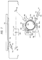
- the photosensitive member 101 is uniformly charged by the main charger 102 to which high voltage of + 6 to 8 KV is applied.
- the image forming portion 103 light emitted from a lamp 110 is reflected by an original 112 rested on an original support glass 111, and the reflected light is incident to the photosensitive member 101 through mirrors 113, 114, 115, thereby forming an electrostatic latent image on the photosensitive member 101.
- Toner having negative polarity is supplied from the developing device 104 to the latent image, thereby visualizing the latent image as a toner image.
- An object of the present invention is to prevent toner from adhering to a photosensitive member.
- a still further object of the present invention is to provide an electrophotographing apparatus which can be made cheaper by omitting an electric power supplying mechanism such as a slip ring and the like which was conventionally required for installing a heat source within a photosensitive member.
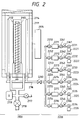
- the toner remaining on the photosensitive member 401 is partially absorbed by a magnet roller 420 of the cleaner 407 and the other residual toner is scraped off from the photosensitive member by a cleaning blade 421 of the cleaner 407.
- the scraped toner is collected into a hopper 430 through a convey screw 431 and is re-used.
- the photosensitive member 401 is polished by a magnetic brush of the magnet roller 420 and the electrostatic latent image remaining on the photosensitive member 401 is erased by the electricity removal light source 409.
- the magnet roller 420 includes a roller, and a magnet brush formed on the roller and contacted with the photosensitive member 401.
- the OPC photosensitive member i.e. surface layer, photo-conductive layer and optional intermediate layer
- the surface layer must endure against high temperature radiation heat from the heater and be prevented from softening. It was found that the mixture of polyester resin having high melting point and curing resin affords both inherent effects of these resins and satisfies the requirements.
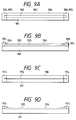
- the electrophotographic photosensitive member 1100 shown in Fig. 11A comprises a support 1101 and a photosensitive layer 1102 formed on the support.
- the photosensitive layer 1102 is constituted by a-Si:H,X and has a photo-conductive layer 1103 having photo-conductivity.
- Si silicon atoms
- H hydrogen atoms
- X halogen supplying raw material gas capable of supplying halogen atoms
- the noncrystalline materials for forming the photo-conductive layer 1103 and the surface layer 1104 (which layers constitute the photosensitive layer 1102) have common factor (silicon atoms), chemical stability is fully ensured at interface between the layers.
- the photosensitive member formed with hydrogen atoms and/or fluorine atoms having the contents as indicated above is excellently superior to the conventional photosensitive members with respect to practical use and can be fully utilized. That is to say, it is known that the defects mainly, dangling bond of silicon atoms and/or carbon atoms) affect a bad influence upon the feature of the electrophotographic photosensitive member.
- such bad influence includes deterioration of the charging feature due to injection of charges from free surface, fluctuation of charging feature due to the change in structure of layers under the usage environment (for example, high humidity condition), and occurrence of residual image due to the repeated use during which the charges are injected into the surface layer from the photo-conductive layer in the corona charging and light illumination and the charges are trapped in the defects (damaged portions) of the surface layer.
- Materials for providing silicon (Si) supplying gas used in the formation of the surface layer 1104 of the present invention may be silicon hydride (silane class) which is maintained in a gaseous condition or can be gasified, such as SiH4, Si2H6, Si3H6, Si3H8, Si4H10 or the like. Among them, SiH4 and Si2H6 are preferable in the points that they can be easily handled during the layer formation and they have good Si supplying rate. Further, Si supplying raw material gas may be diluted by hydrogen gas (H2), helium gas (He), argon gas (Ar) or neon gas (Ne), if necessary.
- H2H6, Si3H6, Si3H8, Si4H10 silicon hydride
- SiH4 and Si2H6 are preferable in the points that they can be easily handled during the layer formation and they have good Si supplying rate.
- Si supplying raw material gas may be diluted by hydrogen gas (H2), helium gas (He), argon gas (Ar) or neon gas
- Materials for providing nitrogen or oxygen supplying gas may be compound which is maintained in a gaseous condition or can be gasified, such as NH3, NO, N2O, NO2, H2O, O2, CO, CO2, N2 or the like. Further, the carbon supplying raw material gas may be diluted by hydrogen gas (H2), helium gas (He), argon gas (Ar) or neon gas (Ne), if necessary.
- H2 hydrogen gas
- He helium gas
- Ar argon gas
- Ne neon gas
- the IIIb group atoms may be boron (B), aluminum (Al), gallium (Ga), indium (In) or thallium (Tl), and, particularly, B, Al and Ga are preferable.
- the Vb group atoms may be phosphorus (P), arsenic (As), antimony (Sb) or bismuth (Bi), and, particularly, P and As are preferable.
- the formation of the deposit film is performed by using the above-mentioned manufacturing apparatus, for example, in the following manner.
- a main valve 2118 is opened to discharge air from the reaction vessel 2111 and a gas piping 2116.
- This manufacturing apparatus generally comprises a reaction vessel 3111 of vacuum fluid-tight type wherein pressure in the vessel can be reduced, a raw material gas supplying device 2200, and a discharge device (not shown) for reducing pressure in a reaction vessel 3111.
- Cylindrical supports 3112, heaters 3113 for heating the supports, a raw material gas introduction conduit 3114 and an electrode 3115 are disposed within the reaction vessel 3111, and a high frequency matching box 3116 is connected to the electrode 3115.
- the interior of the reaction vessel 3111 is connected to a diffusion pump (not shown) through a discharge pipe 3121.
- a desired multilayer photosensitive layer 1102 is formed.
- the flow-in valves other than the required valve(s) are closed.
- the flow-out valves 2251-2256 are closed, the auxiliary valve 2260 is opened and the main valve (not shown) is also fully opened, thereby temporarily discharging the fluid from the apparatus completely by high vacuum.
- the kinds of gasses and valves to be utilized may be changed in accordance with the layer forming condition.
- the temperature of the support 3112 should be set to 200 to 330°C, and preferably 250 to 300°C.
- dimension and configuration of the electrode disposed within the discharging area can be appropriately selected so long as the discharge is not disturbed or distorted, but, in practice, a cylindrical shape having a diameter of 1 mm to 10 cm is preferable. In this case, a length of the electrode can also be appropriately selected so long as the electric field acts on the support uniformly.
- a-Si deposit film having a thickness of about 1 ⁇ m was formed on a glass substrate (Commercial No.: 7059; manufactured by Corning Inc.) and a silicon wafer rested on a circular sample holder in accordance with the photo-conductive layer forming condition.
- An A ⁇ split-type electrode was adhered to the deposit film on the glass substrate by vapor deposition treatment.
- Feature energy (Eu) of an exponential function tail and local level density (D.O.S) were measured by CPM, and hydrogen content of the deposit film on the silicon wafer was measured by FTIP.
- Eu Feature energy
- D.O.S local level density
- the temperature of the photosensitive member is adjusted to 40°C, and, regarding the temperature difference A, the temperature of the surface of the photosensitive member and the temperature of a back surface of the substrate were measured by a thermocouple.
- the temperature difference is represented by a difference in temperature of these surfaces when the temperature of the back surface of the substrate reaches (room temperature + 10°C) after the heating is started [(photosensitive member surface temperature °C) - (substrate back surface temperature °C)].
- the present invention it is possible to eliminate the various drawbacks caused by the conventional electrophotographic photosensitive members constituted by OPC and a-Si, and the excellent electrical feature, optical feature, photo-conductive feature, image feature, durability and usage environmental feature can be achieved.
Landscapes
- General Physics & Mathematics (AREA)
- Physics & Mathematics (AREA)
- Environmental & Geological Engineering (AREA)
- Engineering & Computer Science (AREA)
- Life Sciences & Earth Sciences (AREA)
- Ecology (AREA)
- Environmental Sciences (AREA)
- Biodiversity & Conservation Biology (AREA)
- Atmospheric Sciences (AREA)
- Sustainable Development (AREA)
- Photoreceptors In Electrophotography (AREA)
- Cleaning In Electrography (AREA)
- Discharging, Photosensitive Material Shape In Electrophotography (AREA)
- Electrostatic Charge, Transfer And Separation In Electrography (AREA)
- Control Or Security For Electrophotography (AREA)
- Developing Agents For Electrophotography (AREA)
Applications Claiming Priority (3)
| Application Number | Priority Date | Filing Date | Title |
|---|---|---|---|
| JP303644/94 | 1994-12-07 | ||
| JP30364494A JP3149075B2 (ja) | 1994-12-07 | 1994-12-07 | 電子写真装置 |
| JP30364494 | 1994-12-07 |
Publications (3)
| Publication Number | Publication Date |
|---|---|
| EP0718723A2 true EP0718723A2 (fr) | 1996-06-26 |
| EP0718723A3 EP0718723A3 (fr) | 1997-11-05 |
| EP0718723B1 EP0718723B1 (fr) | 2002-05-02 |
Family
ID=17923487
Family Applications (1)
| Application Number | Title | Priority Date | Filing Date |
|---|---|---|---|
| EP95119212A Expired - Lifetime EP0718723B1 (fr) | 1994-12-07 | 1995-12-06 | Appareil électrophotographique |
Country Status (6)
| Country | Link |
|---|---|
| US (1) | US5689768A (fr) |
| EP (1) | EP0718723B1 (fr) |
| JP (1) | JP3149075B2 (fr) |
| KR (1) | KR0175117B1 (fr) |
| CN (1) | CN1083999C (fr) |
| DE (1) | DE69526566T2 (fr) |
Families Citing this family (16)
| Publication number | Priority date | Publication date | Assignee | Title |
|---|---|---|---|---|
| CN1143180C (zh) * | 1997-05-23 | 2004-03-24 | 富士施乐株式会社 | 显影设备及使用该显影设备的成像设备 |
| KR100262513B1 (ko) | 1998-05-19 | 2000-08-01 | 윤종용 | 용지 함습 검출에 의한 전사 조건 최적화 장치 및 방법 |
| JP3976955B2 (ja) | 1999-09-06 | 2007-09-19 | キヤノン株式会社 | 電子写真方法 |
| JP3507406B2 (ja) | 2000-05-12 | 2004-03-15 | キヤノン株式会社 | 画像形成方法および感光体 |
| US6963720B2 (en) * | 2001-09-03 | 2005-11-08 | Konica Corporation | Image forming method and image forming apparatus with toner having specific characteristic |
| JP3875977B2 (ja) * | 2004-03-03 | 2007-01-31 | シャープ株式会社 | 電子写真感光体用塗料組成物、電子写真感光体の製造方法、電子写真感光体および画像形成装置 |
| JP2006189489A (ja) | 2004-12-28 | 2006-07-20 | Canon Inc | 画像形成装置 |
| US9017480B2 (en) * | 2006-04-06 | 2015-04-28 | First Solar, Inc. | System and method for transport |
| JP4850619B2 (ja) * | 2006-08-14 | 2012-01-11 | キヤノン株式会社 | 画像形成装置 |
| US9615463B2 (en) * | 2006-09-22 | 2017-04-04 | Oscar Khaselev | Method for producing a high-aspect ratio conductive pattern on a substrate |
| US7851113B2 (en) * | 2006-11-01 | 2010-12-14 | Xerox Corporation | Electrophotographic photoreceptors having reduced torque and improved mechanical robustness |
| JP5404295B2 (ja) * | 2008-11-28 | 2014-01-29 | キヤノン株式会社 | コロナ帯電器を備える画像形成装置 |
| JP5810111B2 (ja) * | 2013-02-15 | 2015-11-11 | 京セラドキュメントソリューションズ株式会社 | 画像形成装置 |
| JP5927130B2 (ja) * | 2013-02-15 | 2016-05-25 | 京セラドキュメントソリューションズ株式会社 | 画像形成装置 |
| JP5823445B2 (ja) * | 2013-06-07 | 2015-11-25 | 京セラドキュメントソリューションズ株式会社 | 画像形成装置 |
| US10197950B2 (en) * | 2015-07-31 | 2019-02-05 | Hp Indigo B.V. | Generating mixed ink in a printing press |
Citations (19)
| Publication number | Priority date | Publication date | Assignee | Title |
|---|---|---|---|---|
| US2297692A (en) | 1939-08-15 | 1942-10-06 | Bendix Aviat Corp | Fluid flywheel control |
| JPS5483746A (en) | 1977-12-16 | 1979-07-04 | Nippon Gakki Seizo Kk | Amplifier circuit |
| JPS5711556A (en) | 1980-06-26 | 1982-01-21 | Mitsubishi Electric Corp | Data transfer system |
| JPS57158650A (en) | 1981-03-25 | 1982-09-30 | Minolta Camera Co Ltd | Amorphous silicon photoconductor layer |
| JPS59111179A (ja) | 1982-12-16 | 1984-06-27 | Canon Inc | 画像乱れ防止方法 |
| JPS6067951A (ja) | 1983-09-22 | 1985-04-18 | Minolta Camera Co Ltd | 感光体 |
| JPS6095551A (ja) | 1983-10-31 | 1985-05-28 | Mita Ind Co Ltd | 電子写真方法 |
| JPS6035059B2 (ja) | 1977-12-22 | 1985-08-12 | キヤノン株式会社 | 電子写真感光体およびその製造方法 |
| JPS60168156A (ja) | 1984-02-13 | 1985-08-31 | Canon Inc | 光受容部材 |
| JPS60178457A (ja) | 1984-02-27 | 1985-09-12 | Canon Inc | 光受容部材 |
| JPS60225854A (ja) | 1984-04-24 | 1985-11-11 | Canon Inc | 光受容部材用の支持体及び光受容部材 |
| JPS61100780A (ja) | 1984-10-23 | 1986-05-19 | Canon Inc | クリ−ニング装置 |
| JPS61231561A (ja) | 1985-04-06 | 1986-10-15 | Canon Inc | 光導電部材用の支持体及び該支持体を有する光導電部材 |
| JPS62168161A (ja) | 1986-01-20 | 1987-07-24 | Canon Inc | 電子写真用光受容部材 |
| JPS62278577A (ja) | 1986-05-27 | 1987-12-03 | Fuji Xerox Co Ltd | 電子写真複写装置 |
| JPS6434205U (fr) | 1987-08-24 | 1989-03-02 | ||
| JPH0238956B2 (fr) | 1984-07-26 | 1990-09-03 | Canon Kk | |
| JPH04223910A (ja) | 1990-04-11 | 1992-08-13 | Grapha Holding Ag | 把持具 |
| JPH04324748A (ja) | 1991-04-24 | 1992-11-13 | Canon Inc | 画像通信装置 |
Family Cites Families (12)
| Publication number | Priority date | Publication date | Assignee | Title |
|---|---|---|---|---|
| NL7312451A (fr) * | 1972-09-16 | 1974-02-25 | ||
| JPS5346096B2 (fr) * | 1973-04-02 | 1978-12-11 | ||
| AU530905B2 (en) * | 1977-12-22 | 1983-08-04 | Canon Kabushiki Kaisha | Electrophotographic photosensitive member |
| US4464672A (en) * | 1982-06-15 | 1984-08-07 | Minnesota Mining And Manufacturing Company | Electrographic recording apparatus |
| JPS6173984A (ja) * | 1984-09-20 | 1986-04-16 | Casio Comput Co Ltd | クリ−ニング装置 |
| JPS6236676A (ja) * | 1985-08-10 | 1987-02-17 | Canon Inc | 光導電部材用の支持体及び該支持体を有する光導電部材 |
| US4721663A (en) * | 1985-08-26 | 1988-01-26 | Energy Conversion Devices, Inc. | Enhancement layer for negatively charged electrophotographic devices |
| US4791455A (en) * | 1986-02-13 | 1988-12-13 | Matsushita Electric Industrial Co., Ltd. | Color electrophotographic apparatus and method of cleaning a photosensitive medium |
| JP2686857B2 (ja) * | 1991-05-13 | 1997-12-08 | 沖電気工業株式会社 | 電子写真記録装置 |
| JP3183733B2 (ja) * | 1992-11-26 | 2001-07-09 | 株式会社リコー | 画像形成装置の廃トナー検知装置 |
| US5442430A (en) * | 1993-06-16 | 1995-08-15 | Ricoh Company, Ltd. | Color image forming apparatus and cleaning device therefor |
| JPH07230177A (ja) * | 1993-12-22 | 1995-08-29 | Canon Inc | 電子写真感光体、その製造方法及び該電子写真感光体を有する電子写真装置 |
-
1994
- 1994-12-07 JP JP30364494A patent/JP3149075B2/ja not_active Expired - Fee Related
-
1995
- 1995-12-06 US US08/568,268 patent/US5689768A/en not_active Expired - Lifetime
- 1995-12-06 EP EP95119212A patent/EP0718723B1/fr not_active Expired - Lifetime
- 1995-12-06 DE DE69526566T patent/DE69526566T2/de not_active Expired - Fee Related
- 1995-12-07 KR KR1019950047341A patent/KR0175117B1/ko not_active Expired - Fee Related
- 1995-12-07 CN CN95120234A patent/CN1083999C/zh not_active Expired - Fee Related
Patent Citations (19)
| Publication number | Priority date | Publication date | Assignee | Title |
|---|---|---|---|---|
| US2297692A (en) | 1939-08-15 | 1942-10-06 | Bendix Aviat Corp | Fluid flywheel control |
| JPS5483746A (en) | 1977-12-16 | 1979-07-04 | Nippon Gakki Seizo Kk | Amplifier circuit |
| JPS6035059B2 (ja) | 1977-12-22 | 1985-08-12 | キヤノン株式会社 | 電子写真感光体およびその製造方法 |
| JPS5711556A (en) | 1980-06-26 | 1982-01-21 | Mitsubishi Electric Corp | Data transfer system |
| JPS57158650A (en) | 1981-03-25 | 1982-09-30 | Minolta Camera Co Ltd | Amorphous silicon photoconductor layer |
| JPS59111179A (ja) | 1982-12-16 | 1984-06-27 | Canon Inc | 画像乱れ防止方法 |
| JPS6067951A (ja) | 1983-09-22 | 1985-04-18 | Minolta Camera Co Ltd | 感光体 |
| JPS6095551A (ja) | 1983-10-31 | 1985-05-28 | Mita Ind Co Ltd | 電子写真方法 |
| JPS60168156A (ja) | 1984-02-13 | 1985-08-31 | Canon Inc | 光受容部材 |
| JPS60178457A (ja) | 1984-02-27 | 1985-09-12 | Canon Inc | 光受容部材 |
| JPS60225854A (ja) | 1984-04-24 | 1985-11-11 | Canon Inc | 光受容部材用の支持体及び光受容部材 |
| JPH0238956B2 (fr) | 1984-07-26 | 1990-09-03 | Canon Kk | |
| JPS61100780A (ja) | 1984-10-23 | 1986-05-19 | Canon Inc | クリ−ニング装置 |
| JPS61231561A (ja) | 1985-04-06 | 1986-10-15 | Canon Inc | 光導電部材用の支持体及び該支持体を有する光導電部材 |
| JPS62168161A (ja) | 1986-01-20 | 1987-07-24 | Canon Inc | 電子写真用光受容部材 |
| JPS62278577A (ja) | 1986-05-27 | 1987-12-03 | Fuji Xerox Co Ltd | 電子写真複写装置 |
| JPS6434205U (fr) | 1987-08-24 | 1989-03-02 | ||
| JPH04223910A (ja) | 1990-04-11 | 1992-08-13 | Grapha Holding Ag | 把持具 |
| JPH04324748A (ja) | 1991-04-24 | 1992-11-13 | Canon Inc | 画像通信装置 |
Also Published As
| Publication number | Publication date |
|---|---|
| CN1132864A (zh) | 1996-10-09 |
| DE69526566T2 (de) | 2003-03-27 |
| KR960024754A (ko) | 1996-07-20 |
| KR0175117B1 (ko) | 1999-04-01 |
| DE69526566D1 (de) | 2002-06-06 |
| US5689768A (en) | 1997-11-18 |
| JP3149075B2 (ja) | 2001-03-26 |
| JPH08160821A (ja) | 1996-06-21 |
| CN1083999C (zh) | 2002-05-01 |
| EP0718723A3 (fr) | 1997-11-05 |
| EP0718723B1 (fr) | 2002-05-02 |
Similar Documents
| Publication | Publication Date | Title |
|---|---|---|
| EP0718723B1 (fr) | Appareil électrophotographique | |
| JP3302326B2 (ja) | 画像形成装置 | |
| EP0953883A1 (fr) | Elément photosensitible à utiliser dans un appareil de procédé de formation d'images et appareil de procédé de formation d'images comprenant un tel élément photosensible | |
| EP0762229B1 (fr) | Appareil de formation d'images et procédé de formation d'images | |
| JP2002229303A (ja) | 電子写真装置 | |
| JP3128186B2 (ja) | 電子写真装置 | |
| US5732313A (en) | Charge apparatus and image forming apparatus | |
| JPH08272190A (ja) | 帯電装置および画像形成装置 | |
| JP3535664B2 (ja) | 電子写真装置 | |
| JP3247283B2 (ja) | 帯電装置及び画像形成装置 | |
| JPH08272194A (ja) | 帯電装置および画像形成装置 | |
| JP3559665B2 (ja) | 画像形成装置 | |
| JP3221274B2 (ja) | 画像形成装置 | |
| JPH08171262A (ja) | 帯電部材とこれを用いた帯電装置及び画像形成装置 | |
| JP2000094736A (ja) | 電子写真装置および電子写真方法 | |
| JP3545925B2 (ja) | 画像形成装置 | |
| JP2000131924A (ja) | 帯電部材とこの帯電部材を用いた画像形成装置 | |
| JPH11143176A (ja) | 帯電部材および画像形成装置 | |
| JPH09222773A (ja) | 磁気ブラシ帯電装置、画像形成装置及びプロセスカートリッヂ | |
| JPH09222772A (ja) | 帯電部材、帯電装置、画像形成装置及びプロセスカートリッヂ | |
| JPH08227260A (ja) | 電子写真装置の除湿装置 | |
| JPH1031344A (ja) | 帯電装置および画像形成装置 | |
| JPH08234540A (ja) | 画像形成装置 | |
| JPH10240017A (ja) | 画像形成装置 | |
| JPH09325566A (ja) | 帯電装置および画像形成装置 |
Legal Events
| Date | Code | Title | Description |
|---|---|---|---|
| PUAI | Public reference made under article 153(3) epc to a published international application that has entered the european phase |
Free format text: ORIGINAL CODE: 0009012 |
|
| AK | Designated contracting states |
Kind code of ref document: A2 Designated state(s): DE FR GB IT |
|
| PUAL | Search report despatched |
Free format text: ORIGINAL CODE: 0009013 |
|
| AK | Designated contracting states |
Kind code of ref document: A3 Designated state(s): DE FR GB IT |
|
| 17P | Request for examination filed |
Effective date: 19980327 |
|
| 17Q | First examination report despatched |
Effective date: 20000516 |
|
| GRAG | Despatch of communication of intention to grant |
Free format text: ORIGINAL CODE: EPIDOS AGRA |
|
| GRAG | Despatch of communication of intention to grant |
Free format text: ORIGINAL CODE: EPIDOS AGRA |
|
| GRAH | Despatch of communication of intention to grant a patent |
Free format text: ORIGINAL CODE: EPIDOS IGRA |
|
| REG | Reference to a national code |
Ref country code: GB Ref legal event code: IF02 |
|
| GRAH | Despatch of communication of intention to grant a patent |
Free format text: ORIGINAL CODE: EPIDOS IGRA |
|
| GRAA | (expected) grant |
Free format text: ORIGINAL CODE: 0009210 |
|
| AK | Designated contracting states |
Kind code of ref document: B1 Designated state(s): DE FR GB IT |
|
| REG | Reference to a national code |
Ref country code: GB Ref legal event code: FG4D |
|
| REF | Corresponds to: |
Ref document number: 69526566 Country of ref document: DE Date of ref document: 20020606 |
|
| ET | Fr: translation filed | ||
| PLBE | No opposition filed within time limit |
Free format text: ORIGINAL CODE: 0009261 |
|
| STAA | Information on the status of an ep patent application or granted ep patent |
Free format text: STATUS: NO OPPOSITION FILED WITHIN TIME LIMIT |
|
| 26N | No opposition filed |
Effective date: 20030204 |
|
| PGFP | Annual fee paid to national office [announced via postgrant information from national office to epo] |
Ref country code: GB Payment date: 20041201 Year of fee payment: 10 |
|
| PGFP | Annual fee paid to national office [announced via postgrant information from national office to epo] |
Ref country code: DE Payment date: 20041202 Year of fee payment: 10 |
|
| PGFP | Annual fee paid to national office [announced via postgrant information from national office to epo] |
Ref country code: FR Payment date: 20041208 Year of fee payment: 10 |
|
| PG25 | Lapsed in a contracting state [announced via postgrant information from national office to epo] |
Ref country code: IT Free format text: LAPSE BECAUSE OF NON-PAYMENT OF DUE FEES;WARNING: LAPSES OF ITALIAN PATENTS WITH EFFECTIVE DATE BEFORE 2007 MAY HAVE OCCURRED AT ANY TIME BEFORE 2007. THE CORRECT EFFECTIVE DATE MAY BE DIFFERENT FROM THE ONE RECORDED. Effective date: 20051206 Ref country code: GB Free format text: LAPSE BECAUSE OF NON-PAYMENT OF DUE FEES Effective date: 20051206 |
|
| PG25 | Lapsed in a contracting state [announced via postgrant information from national office to epo] |
Ref country code: DE Free format text: LAPSE BECAUSE OF NON-PAYMENT OF DUE FEES Effective date: 20060701 |
|
| GBPC | Gb: european patent ceased through non-payment of renewal fee |
Effective date: 20051206 |
|
| PG25 | Lapsed in a contracting state [announced via postgrant information from national office to epo] |
Ref country code: FR Free format text: LAPSE BECAUSE OF NON-PAYMENT OF DUE FEES Effective date: 20060831 |
|
| REG | Reference to a national code |
Ref country code: FR Ref legal event code: ST Effective date: 20060831 |