EP0724207A2 - Détection des pertubations dans un signal d'horloge basée sur le rapport entre les périodes de l'horloge principale des sous-horloges - Google Patents
Détection des pertubations dans un signal d'horloge basée sur le rapport entre les périodes de l'horloge principale des sous-horloges Download PDFInfo
- Publication number
- EP0724207A2 EP0724207A2 EP96101114A EP96101114A EP0724207A2 EP 0724207 A2 EP0724207 A2 EP 0724207A2 EP 96101114 A EP96101114 A EP 96101114A EP 96101114 A EP96101114 A EP 96101114A EP 0724207 A2 EP0724207 A2 EP 0724207A2
- Authority
- EP
- European Patent Office
- Prior art keywords
- pulse signal
- signal
- polarity
- disturbance
- timing
- Prior art date
- Legal status (The legal status is an assumption and is not a legal conclusion. Google has not performed a legal analysis and makes no representation as to the accuracy of the status listed.)
- Withdrawn
Links
Images

Classifications
-
- H—ELECTRICITY
- H03—ELECTRONIC CIRCUITRY
- H03K—PULSE TECHNIQUE
- H03K5/00—Manipulating of pulses not covered by one of the other main groups of this subclass
- H03K5/19—Monitoring patterns of pulse trains
-
- G—PHYSICS
- G06—COMPUTING OR CALCULATING; COUNTING
- G06F—ELECTRIC DIGITAL DATA PROCESSING
- G06F1/00—Details not covered by groups G06F3/00 - G06F13/00 and G06F21/00
- G06F1/04—Generating or distributing clock signals or signals derived directly therefrom
Definitions
- the present invention generally relates to a clock monitor circuit, and in particular to a circuit for detecting a clock disturbance which occurs due to the mixing of similar pulses into or lack of necessary pulses of a bipolar clock signal.
- a bipolar clock generally consists of a pulse stream with the polarity alternating in time as follows: +1, 0, -1, 0, +1, and so on.
- a bipolar violation method that the polarity alternation order is violated in a predetermined period like this: +1, 0, +1, 0, -1, 0, and so on.
- Such a bipolar violation method is frequently employed to superpose a subclock on a main clock.
- a clock extractor extracts the subclock from the bipolar clock and supplies it as a reference phase clock to a data processing circuit. For such a clock extractor, a clock monitor circuit is necessary to avoid recognizing a pulse disturbance as the bipolar violation.
- a clock extracting circuit employing the bipolar violation method is disclosed in Japanese Patent Unexamined Publication No. 3-272245.
- a positive-polarity pulse detector 1 detects a positive-pulse signal S1 from the bipolar clock signal by comparing the bipolar clock signal with a first reference voltage Ref-p.
- a negative-polarity pulse detector 2 detects a negative-pulse signal S2 from the bipolar clock signal by comparing the bipolar clock signal with a second reference voltage Ref-n.
- a bipolar violation detector 3 receives them to detect the subclock signal.
- the clock extracting circuit further includes a clock monitor circuit comprising two counters 4 and 5 and a comparator 6.
- the respective counters 4 and 5 count pulses of the positive-pulse signal S1 and the negative-pulse signal S2 while concurrently reset in a predetermined period.
- the comparator 6 compares the resultant count values of the counters 4 and 5 in the predetermined period and produces an alarm signal when the count difference is larger than predetermined.
- the conventional clock monitor circuit cannot detect a clock disturbance in cases where equal numbers of pulses are mixed into or removed from both the positive-pulse signal S1 and the negative-pulse signal S2. Because the conventional clock monitor circuit detects the clock disturbance based on the count difference between the counters 4 and 5 separately counting positive pulses and negative pulses, respectively.
- An object of the present invention is to provide a clock monitor circuit which detects a clock disturbance with reliability.
- Another object of the present invention is to provide a clock disturbance detecting circuit and method which properly detect a clock disturbance such as a case where the positive- and negative-pulses both change in number.
- a first-polarity pulse signal and a second-polarity pulse signal are produced from a bipolar pulse signal including a main pulse signal and a subpulse signal.
- the period of the subpulse signal is a predetermined integral multiple of that of the main pulse signal.
- a first disturbance is detected from the first-polarity pulse signal by checking whether a first pulse signal coincides with a second pulse signal using said second-polarity pulse signal as a first timing signal.
- the first pulse signal corresponds to the first-polarity pulse signal at a first timing instant and the second pulse signal corresponds to the first-polarity pulse signal at a second timing instant.
- the timing difference between the first and second timing instants corresponds to the period ratio of the main pulse signal and the subpulse signal.
- the first disturbance is detected when the first pulse signal does not coincide with the second pulse signal.
- a circuit is comprised of a shift register which shifts first data corresponding to the first-polarity pulse signal in accordance with the first timing signal to produce the first pulse signal and the second pulse signal.
- the circuit is further comprised of a coincidence checking circuit which checks whether the first pulse signal coincides with the second pulse signal to produce a first detection signal indicating the first disturbance when the first pulse signal is not identical with the second pulse signal.
- the circuit is further comprised of a shift register which shifts second data corresponding to the second-polarity pulse signal using the second-polarity pulse signal as a second timing signal and produces the third pulse signal and the fourth pulse signal.
- the circuit is still further comprised of a coincidence checking circuit which checks whether the third pulse signal coincides with the fourth pulse signal to produce a second detection signal indicating the second disturbance when the third pulse signal is not identical with the fourth pulse signal.
- the circuit is still more further comprised of an output circuit for producing a detection signal of the bipolar pulse disturbance based on the first disturbance and the second disturbance.
- the output circuit is a logical-OR circuit which receives the first disturbance and the second disturbance.
- the shift register shifts the data according to the second-polarity pulse signal and the data stored in the sift register always has a predetermined repetition period of the subpulse, the first data and the second data are identical at all times.
- the pulse repetition order is vanished, resulting in non-coincidence between the first data and the second data of the shift register. Therefore, the disturbance signal is produced by the comparator when a bipolar pulse disturbance occurs. Since the logical-OR circuit receives the first disturbance signal and the second disturbance signal, the circuit detects the bipolar pulse disturbance when at least one of the first disturbance signal and the second disturbance signal occurs.
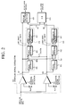
- a clock extractor receives a bipolar clock signal BCL including a main clock of a period T m and a subclock of a period T sub superposed on the main clock and produces the subclock and an alarm signal which indicates a clock disturbance.
- the clock extractor is comprised of a unipolar signal extractor 100 including a positive-polarity pulse detector 101 and a negative-polarity pulse detector 102 which receive the bipolar clock signal BCL and produce a positive-polarity pulse signal SP and a negative-polarity pulse signal SN, respectively.
- the positive-polarity pulse detector 101 detects the positive-polarity pulse signal SP from the bipolar clock signal BCL by comparing the bipolar clock signal BCL with the first reference voltage Ref-p.
- the negative-polarity pulse detector 102 detects the negative-polarity pulse signal SN from the bipolar clock signal BCL by comparing the bipolar clock signal BCL with the second reference voltage Ref-n.
- the positive-polarity and negative-polarity pulse detectors 101 and 102 are both formed with a differential amplifier.
- a bipolar violation detector 103 receives the positive-polarity and negative-polarity pulse signals SP and SN and reproduces the subclock signal superposed on the bipolar clock signal BCL.
- the clock extractor is further provided with a first error detector 104, a second error detector 105, and an OR circuit 106.
- the first error detector 104 and the second error detector 105 receive the positive-polarity and negative-polarity pulse signals SP and SN, respectively, and output a first error signal E1 and a second error signal E2 to the OR circuit 106.
- the OR circuit produces the alarm signal when receiving at least one of the first error signal E1 and the second error signal E2.
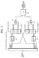
- the first error detector 104 is comprised of a frequency divider 201, a shift register 202, and a non-coincidence determination circuit 103.
- the frequency divider 201 divides the positive-polarity pulse signal SP in frequency to output the divided signal SPd to the shift register 202.
- the shift register 202 receives the divided signal SPd as data, the shift register 202 shifts the data in accordance with the negative-polarity pulse signal SN which is received as a shift clock from the negative-polarity pulse detector 102.
- the shift register 202 outputs first data shifted by i bits and second data shifted by j bits to the non-coincidence determination circuit 203, where i and j are a positive integer and are determined based on a ratio of the periods T m and T sub of the main clock and the subclock as described later.
- the non-coincidence determination circuit 203 receives the first data and the second data from the shift register 202 and outputs the error signal E1 to the OR circuit 106 when the first data is not identical with the second data.
- the second error detector 105 is comprised of a frequency divider 301, a shift register 302, and a non-coincidence determination circuit 303.
- the frequency divider 301 divides the negative-polarity pulse signal SN in frequency to output the divided signal SNd to the shift register 302.
- the shift register 302 receives the divided signal SNd as data, the shift register 302 shifts the data in accordance with the positive-polarity pulse signal SP which is received as a shift clock from the positive-polarity pulse detector 101.
- the shift register 302 outputs third data shifted by k bits and fourth data shifted by l bits to the non-coincidence determination circuit 303, where k and l are a positive integer and are determined based on a ratio of the periods T m and T sub of the main clock and the subclock as described later.
- the non-coincidence determination circuit 303 receives the third data and the fourth data from the shift register 302 and outputs the error signal E2 to the OR circuit 106 when the third data and the fourth data are not identical.
- the frequency divider 201 divides the positive-polarity pulse signal SP in frequency by two and outputs the divided signal SPd to the serial input terminal of the shift register 202.
- the shift register 202 has two parallel output terminals corresponding to the i-bit shift and the (i+8)-bit shift, respectively. In this case, it is assumed that the period T sub of the subclock is 8 times the period T m of the main clock.
- the stored data is shifted in accordance with the negative-polarity pulse signal SN which is received as a shift clock from the negative-polarity pulse detector 102.
- the shift register 202 outputs the first data shifted by i bits and the second data shifted by i+8 bits in parallel to an exclusive-OR circuit 203 which serves as the non-coincidence determination circuit.
- the exclusive-OR circuit 203 receives the first data and the second data from the shift register 202, the exclusive-OR circuit 203 outputs the error signal E1 to the OR circuit 106 when the first data is not identical with the second data.
- the second error detector 105 has the same circuit configuration as the first error detector 104 except that the shift register 302 operates in accordance with the positive-polarity pulse signal SP serving as a shift clock.
- the shift register 302 outputs the third data shifted by k bits and the fourth data shifted by k+8 bits in parallel to an exclusive-OR circuit 303 which outputs the error signal E2 to the OR circuit 106 when the third data is not identical with the fourth data.
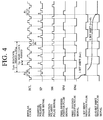
- an operation of the clock monitor circuit will be described hereinafter.
- the positive-polarity pulse signal SP and the negative-polarity pulse signal SN each having a repetition period 2T sub are output to the frequency dividers 201 and 301, respectively.
- the frequency divider 301 divides the negative-polarity pulse signal SN in frequency by two to output the divided pulse signal SNd to the shift register 302.
- the shift register 302 shifts the data according to the positive-polarity pulse signal SP and the divided-by-2 pulse signal SNd always has the repetition period 2T sub , the third data shifted by 1 bit and the fourth data shifted by 1+8 bits are identical at all times as shown in Fig. 4.
- the pulse repetition order is vanished, resulting in non-coincidence between the 1-bit-shift data and the (1+8)-bit-shift data of the shift register 302. Therefore, the error signal E2 of a logical high value is output from the exclusive-OR circuit 303 to the OR circuit 106 when a clock disturbance occurs.
- the first error detector 104 performs the similar operation to the second error detector 105. Since the OR circuit 106 outputs a clock disturbance detection signal of a logical high value when at least one of the error signals E1 and E2 goes high, a bipolar clock disturbance can be detected with reliability even when the same clock disturbance occurs in both the positive-polarity and the negative-polarity pulses.
Landscapes
- Physics & Mathematics (AREA)
- Engineering & Computer Science (AREA)
- Theoretical Computer Science (AREA)
- Nonlinear Science (AREA)
- General Engineering & Computer Science (AREA)
- General Physics & Mathematics (AREA)
- Dc Digital Transmission (AREA)
- Synchronisation In Digital Transmission Systems (AREA)
Applications Claiming Priority (3)
| Application Number | Priority Date | Filing Date | Title |
|---|---|---|---|
| JP1160195 | 1995-01-27 | ||
| JP7011601A JP2988300B2 (ja) | 1995-01-27 | 1995-01-27 | バイポーラクロック擾乱検出回路 |
| JP11601/95 | 1995-01-27 |
Publications (2)
| Publication Number | Publication Date |
|---|---|
| EP0724207A2 true EP0724207A2 (fr) | 1996-07-31 |
| EP0724207A3 EP0724207A3 (fr) | 1999-11-24 |
Family
ID=11782431
Family Applications (1)
| Application Number | Title | Priority Date | Filing Date |
|---|---|---|---|
| EP96101114A Withdrawn EP0724207A3 (fr) | 1995-01-27 | 1996-01-26 | Détection des pertubations dans un signal d'horloge basée sur le rapport entre les périodes de l'horloge principale des sous-horloges |
Country Status (3)
| Country | Link |
|---|---|
| US (1) | US5832033A (fr) |
| EP (1) | EP0724207A3 (fr) |
| JP (1) | JP2988300B2 (fr) |
Families Citing this family (2)
| Publication number | Priority date | Publication date | Assignee | Title |
|---|---|---|---|---|
| JP3489560B2 (ja) * | 2000-11-10 | 2004-01-19 | 日本電気株式会社 | クロック断検出回路 |
| US7454645B2 (en) * | 2005-03-31 | 2008-11-18 | Cypress Semiconductor Corp. | Circuit and method for monitoring the status of a clock signal |
Family Cites Families (11)
| Publication number | Priority date | Publication date | Assignee | Title |
|---|---|---|---|---|
| US3938082A (en) * | 1974-09-19 | 1976-02-10 | General Electric Company | Receiver for bi-polar coded data with bit time interval detection used as the data validation discriminant |
| US4001578A (en) * | 1975-08-01 | 1977-01-04 | Bell Telephone Laboratories, Incorporated | Optical communication system with bipolar input signal |
| US4006304A (en) * | 1975-12-10 | 1977-02-01 | Bell Telephone Laboratories, Incorporated | Apparatus for word synchronization in an optical communication system |
| US4086566A (en) * | 1976-11-15 | 1978-04-25 | Gte Automatic Electric Laboratories Incorporated | Error detector for modified duobinary signals |
| JPS59223038A (ja) * | 1983-06-01 | 1984-12-14 | Nec Corp | デ−タ伝送方式 |
| US4750179A (en) * | 1986-05-02 | 1988-06-07 | Lynch Communications Systems, Inc. | Selective prevention of bipolar violation detection |
| JPS63222519A (ja) * | 1987-03-12 | 1988-09-16 | Fujitsu Ltd | B8zs/b6zs符号回路 |
| JPH03187647A (ja) * | 1989-12-18 | 1991-08-15 | Matsushita Electric Ind Co Ltd | 平衡伝送用受信装置 |
| JPH03272245A (ja) * | 1990-03-20 | 1991-12-03 | Fujitsu Ltd | バイポーラバイオレーション検出回路 |
| JP2947003B2 (ja) * | 1993-05-26 | 1999-09-13 | 日本電気株式会社 | バイポーラクロック擾乱検出回路 |
| JP2616395B2 (ja) * | 1993-07-28 | 1997-06-04 | 日本電気株式会社 | バイポーラクロック擾乱検出回路 |
-
1995
- 1995-01-27 JP JP7011601A patent/JP2988300B2/ja not_active Expired - Lifetime
-
1996
- 1996-01-26 EP EP96101114A patent/EP0724207A3/fr not_active Withdrawn
- 1996-01-29 US US08/593,212 patent/US5832033A/en not_active Expired - Fee Related
Also Published As
| Publication number | Publication date |
|---|---|
| JP2988300B2 (ja) | 1999-12-13 |
| US5832033A (en) | 1998-11-03 |
| EP0724207A3 (fr) | 1999-11-24 |
| JPH08204760A (ja) | 1996-08-09 |
Similar Documents
| Publication | Publication Date | Title |
|---|---|---|
| US6333646B1 (en) | Abnormal clock detector and abnormal clock detecting apparatus | |
| EP0261428A2 (fr) | Dispositif de récupération d'horloge | |
| US20020008548A1 (en) | Device for detecting abnormality of clock signal | |
| US5832033A (en) | Clock disturbance detection based on ratio of main clock and subclock periods | |
| JPS61148939A (ja) | フレ−ム同期方式 | |
| JP3092729B2 (ja) | ロジックアナライザ | |
| JP3164904B2 (ja) | 入力信号断検出方式 | |
| JPS61239740A (ja) | 同期信号検出装置 | |
| JPH04329721A (ja) | データ受信方法 | |
| JPH0635733A (ja) | スタック検出方式 | |
| JP2616395B2 (ja) | バイポーラクロック擾乱検出回路 | |
| KR930010918B1 (ko) | 분산형 프레임 구조의 병렬 프레임 검출회로 | |
| KR100212051B1 (ko) | 데이타 수신 장치 및 방법 | |
| JPH05191384A (ja) | 誤り率検出回路 | |
| JPH0124386B2 (fr) | ||
| JPH0118607B2 (fr) | ||
| JPH0420138A (ja) | シリアルデータ伝送システム | |
| JPH0316054B2 (fr) | ||
| JPH0687565B2 (ja) | 平衡複流相互接続回線における信号障害検出方式 | |
| JPS5942505B2 (ja) | デ−タ信号検出回路 | |
| JPH08172687A (ja) | クロックの異常検出回路 | |
| JPH05244146A (ja) | フレーム同期検出回路 | |
| KR970019598A (ko) | 비디오엔코더의 비정상 상태판별 및 자동 복구회로 | |
| JPH07115442A (ja) | 伝送路符号の復号化回路 | |
| JPH07250054A (ja) | シリアル通信のビット同期回路及びビット同期方法 |
Legal Events
| Date | Code | Title | Description |
|---|---|---|---|
| PUAI | Public reference made under article 153(3) epc to a published international application that has entered the european phase |
Free format text: ORIGINAL CODE: 0009012 |
|
| AK | Designated contracting states |
Kind code of ref document: A2 Designated state(s): DE FR GB PT |
|
| PUAL | Search report despatched |
Free format text: ORIGINAL CODE: 0009013 |
|
| AK | Designated contracting states |
Kind code of ref document: A3 Designated state(s): DE FR GB PT |
|
| RIC1 | Information provided on ipc code assigned before grant |
Free format text: 6G 06F 1/04 A, 6H 04L 7/02 B, 6H 04L 25/49 B |
|
| 17P | Request for examination filed |
Effective date: 19991018 |
|
| 17Q | First examination report despatched |
Effective date: 20020314 |
|
| STAA | Information on the status of an ep patent application or granted ep patent |
Free format text: STATUS: THE APPLICATION IS DEEMED TO BE WITHDRAWN |
|
| 18D | Application deemed to be withdrawn |
Effective date: 20020725 |