EP0729191B1 - Injecteur conducteur d'électrons pour des diodes émettrices de lumière - Google Patents
Injecteur conducteur d'électrons pour des diodes émettrices de lumière Download PDFInfo
- Publication number
- EP0729191B1 EP0729191B1 EP19960200313 EP96200313A EP0729191B1 EP 0729191 B1 EP0729191 B1 EP 0729191B1 EP 19960200313 EP19960200313 EP 19960200313 EP 96200313 A EP96200313 A EP 96200313A EP 0729191 B1 EP0729191 B1 EP 0729191B1
- Authority
- EP
- European Patent Office
- Prior art keywords
- silicides
- electrode
- light
- rare
- earth metal
- Prior art date
- Legal status (The legal status is an assumption and is not a legal conclusion. Google has not performed a legal analysis and makes no representation as to the accuracy of the status listed.)
- Expired - Lifetime
Links
Images
Classifications
-
- H—ELECTRICITY
- H01—ELECTRIC ELEMENTS
- H01B—CABLES; CONDUCTORS; INSULATORS; SELECTION OF MATERIALS FOR THEIR CONDUCTIVE, INSULATING OR DIELECTRIC PROPERTIES
- H01B1/00—Conductors or conductive bodies characterised by the conductive materials; Selection of materials as conductors
- H01B1/06—Conductors or conductive bodies characterised by the conductive materials; Selection of materials as conductors mainly consisting of other non-metallic substances
-
- H—ELECTRICITY
- H01—ELECTRIC ELEMENTS
- H01B—CABLES; CONDUCTORS; INSULATORS; SELECTION OF MATERIALS FOR THEIR CONDUCTIVE, INSULATING OR DIELECTRIC PROPERTIES
- H01B1/00—Conductors or conductive bodies characterised by the conductive materials; Selection of materials as conductors
- H01B1/04—Conductors or conductive bodies characterised by the conductive materials; Selection of materials as conductors mainly consisting of carbon-silicon compounds, carbon or silicon
-
- H—ELECTRICITY
- H10—SEMICONDUCTOR DEVICES; ELECTRIC SOLID-STATE DEVICES NOT OTHERWISE PROVIDED FOR
- H10K—ORGANIC ELECTRIC SOLID-STATE DEVICES
- H10K50/00—Organic light-emitting devices
- H10K50/80—Constructional details
- H10K50/805—Electrodes
- H10K50/82—Cathodes
-
- H—ELECTRICITY
- H10—SEMICONDUCTOR DEVICES; ELECTRIC SOLID-STATE DEVICES NOT OTHERWISE PROVIDED FOR
- H10K—ORGANIC ELECTRIC SOLID-STATE DEVICES
- H10K2102/00—Constructional details relating to the organic devices covered by this subclass
- H10K2102/301—Details of OLEDs
- H10K2102/321—Inverted OLED, i.e. having cathode between substrate and anode
-
- H—ELECTRICITY
- H10—SEMICONDUCTOR DEVICES; ELECTRIC SOLID-STATE DEVICES NOT OTHERWISE PROVIDED FOR
- H10K—ORGANIC ELECTRIC SOLID-STATE DEVICES
- H10K50/00—Organic light-emitting devices
- H10K50/80—Constructional details
-
- H—ELECTRICITY
- H10—SEMICONDUCTOR DEVICES; ELECTRIC SOLID-STATE DEVICES NOT OTHERWISE PROVIDED FOR
- H10K—ORGANIC ELECTRIC SOLID-STATE DEVICES
- H10K77/00—Constructional details of devices covered by this subclass and not covered by groups H10K10/80, H10K30/80, H10K50/80 or H10K59/80
-
- H—ELECTRICITY
- H10—SEMICONDUCTOR DEVICES; ELECTRIC SOLID-STATE DEVICES NOT OTHERWISE PROVIDED FOR
- H10K—ORGANIC ELECTRIC SOLID-STATE DEVICES
- H10K77/00—Constructional details of devices covered by this subclass and not covered by groups H10K10/80, H10K30/80, H10K50/80 or H10K59/80
- H10K77/10—Substrates, e.g. flexible substrates
Definitions
- the present invention pertains to organic light-emitting diodes and more particularly pertains to a stable metal electrode with a low work function.
- Mg has a work function of 3.7 eV and is a good candidate for the electron injector
- Tang and VanSlyke in Appl. Phys. Lett. Vol. 51, 1987, p. 913-915 described a stability test in which light-emitting diodes with alloyed Mg-Ag cathodes show a steady degradation accompanied by an increase of the drive voltage. Some of the failure is attributed to the degradation of the contacts.
- a thick indium film greater than one micron is used for encapsulation, as described in U.S. Patent No. 5,073,446.
- JP-A-06310280 and a Patent Abstract thereof discloses an electron-injecting electrode for an organic light-emitting element.
- the electrode is formed of a lanthanum boride (LaB6) film on an insulating substrate.
- An organic light-emitting element is formed by deposition over the LaB6 film in sequence of an organic light-emitting layer, a positive hole transporting layer, and a transparent positive electrode.
- LaB6 lanthanum boride
- One of the major shortcomings presented by the conventional organic light-emitting diode structure is the difficulty in achieving monolithic integration, where, for example, an array of organic light-emitting diodes and the driver electronics are fabricated on a single chip.
- the light-emitting diode consists of an electron-injecting metal contact on the front surface of an electroluminescent layer on a conductive glass substrate.
- a semiconductor wafer such as Si
- the light emission through the substrate is prohibited because of the opaqueness of the substrate. Therefore, a light transmissive top electrode is necessary. Since the materials used for the electron injector are highly reactive with oxygen, a thick cathode layer completely encased in several microns of more inert metals such as indium or gold is commonly used, thus light emission through such a top surface is blocked.
- the electron injector is in contact with Si and the hole injector is on top of organic layers
- light emission through the top electrode is possible because a transparent indium-tin oxide layer or a semi-transparent thin gold layer can be used as the anode.
- the low work function metals are either highly reactive with Si and/or act as a fast diffusing species, thus significantly affecting the device performance.
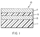
- FIG. 1 is a schematic diagram of an embodiment of the electroluminescence device of the invention.
- an electroluminescence device 10 of the invention has, in order, a substrate 11, a bottom electrode layer 13, an organic layer structure 15, a top electrode layer 17.
- Substrate 11 is a single crystal semiconductor substrate selected from the group consisting of Si, Ge, GaAs, GaP, GaN, GaSb, InAs, InP, InSb, and Al x Ga 1-x AS, where x is from 0 to 1.
- Substrate 11 can be either undoped, lightly doped, or heavily doped.
- Substrate 11 is either bare or covered with a layer of dielectric material such as Si oxides or Si nitrides.
- part of the semiconductor can be used as substrate 11 for electroluminescent device 10, while the remainder of the semiconductor wafer can be processed to form drivers, switchers, or other electronic devices.
- Bottom electrode layer 13 acts as an electron injector having a low work function with a value equal to or less than 4.0 eV and a relatively good stability against atmospheric oxidation. Bottom electrode layer 13 is compatible with substrate 11 showing no interactions with the substrate. Examples 1 and 2 described in this invention indicate that rare-earth metal silicides and yttrium silicides are suitable materials. Chromium borides and lanthanum borides can also be selected for this purpose because of their well known low work functions and stabilities.
- bottom electrode layer 13 is so selected that it is sufficient to form a continuous electrode.
- a useful range of the thickness is from 10 to 1000 nm, preferably 50-500 nm.
- This bottom electrode layer can be deposited by many conventional means, such as metal deposition followed by thermal annealing or hot-substrate deposition on Si to form silicides, sequential deposition of metal and Si, or codeposition of silicides or borides on substrate 11. Deposition can be carried out using evaporation, sputtering, laser ablation, and chemical vapor deposition.
- Organic layer structure 15 either has a single layer acting as a light emitter or a multilayer structure, including a light emitter and carrier-confinement layers.
- a useful structure consists of an undoped or doped Alq 3 layer as the emitter and a diamine layer for hole-transporting, as described in U.S. Patent Nos. 5,294,869, and 5,151,629.
- Suitable materials used for light emitters include poly(paraphenylene vinylene) (PPV), PPV copolymers and derivatives, polyaniline, poly(3-alkylthiophene), poly(3-octylthiophene), poly(paraphenylene), and Alq 3 .
- Organic layer structure 15 can be prepared by thermal evaporation or spin-coating from a solution.
- Top electrode layer 17 acts as a hole injector having a high work function with a value greater than 4.2 eV and good stability in ambient.
- Top electrode layer 17 is either a transparent conducting oxide or a thin metal layer, thus allowing light-emitting from the top surface.
- Suitable metal oxides include indium-tin-oxide, aluminum- or indium-doped zinc oxide, tin oxide, magnesium-indium-oxide, and cadmium-tin-oxide.
- Suitable metals include gold, silver, nickel, palladium, and platinum.
- a transparent encapsulating layer may be needed to protect the organic layered structure from moisture attack.
- the desired metal oxides and metals can be deposited by evaporation, sputtering, laser ablation, and chemical vapor deposition.
- a thickness ranging from 50 to 1000 nm for the metal oxide layer is useful as the hole injector, preferably 100-500 nm; and a thickness ranging from 5 50 nm for the metal layer, preferable 10-30 nm.
- Erbium films were deposited in an electron-beam evaporator with pressures of 1 x 10 -9 Torr prior to deposition, rising to a maximum of 1-2 x 10 -7 Torr during deposition.
- the substrate was heated by a radiative heater consisting of tantalum wires.
- the growth temperature varied between 300-400 °C and was monitored by an infrared pyrometer using published emissivity values.
- the deposition rate was 0.2-0.3 nm ⁇ s -1 and the thickness of the erbium films was about 100 nm.
- Yttrium is known to have a low work function of 3.1 eV, but is strongly reactive with oxygen.
- Yttrium layers with a thickness of 100 nm were deposited on Si encapsulated with thermally grown SiO 2 . Reflections of yttrium were identified after deposition or after post-deposition annealing at 300°C in vacuum. However, the intensity of yttrium reflections decreased significantly and some new peaks developed after 5 days at 100°C, indicating the transformation of yttrium into yttrium oxides. The instability in air would preclude the use of yttrium as a stable contact for electron-injecting.
Landscapes
- Physics & Mathematics (AREA)
- Optics & Photonics (AREA)
- Electroluminescent Light Sources (AREA)
- Led Devices (AREA)
Claims (8)
- Electrode conductrice d'une diode à émission de lumière organique comprenant des siliciures métalliques et ayant un travail de sortie égal ou inférieur à 4,0 eV de sorte que l'électrode procure une bonne stabilité contre la corrosion atmosphérique et agisse comme un injecteur d'électrons pour ladite diode à émission de lumière organique.
- Electrode conductrice selon la revendication 1, dans laquelle lesdits siliciures métalliques sont sélectionnés à partir du groupe des siliciures métalliques de terre rare et des siliciures d'yttrium.
- Electrode conductrice selon la revendication 2, dans laquelle les siliciures métalliques de terre rare incluent le siliciure de dysprosium, les siliciures d'erbium, les siliciures d'europium, les siliciures de gadolinium, les siliciures d'holmium et les siliciures de terbium.
- Electrode conductrice selon la revendication 2, dans laquelle ladite diode à émission de lumière organique inclut une structure constituée dans l'ordre d'une électrode inférieure transmettrice de lumière et conductrice, d'une couche électroluminescente organique et d'une électrode supérieure constituée de siliciure métallique de terre rare ou de siliciure d'yttrium.
- Dispositif électroluminescent ayant des diodes à émission de lumière organiques, comprenant dans l'ordre :un substrat semi-conducteur monocristallin ;l'électrode selon la revendication 1 ;une structure monocouche ou multicouches organique avec certaines des couches agissant comme un émetteur de lumière et le reste servant pour le confinement de porteurs ou le transport de trous ; etune couche d'électrode à injection de trous transmettrice de lumière présentant un travail de sortie égal ou supérieur à 4,2 eV.
- Dispositif électroluminescent selon la revendication 5, dans lequel ledit substrat est sélectionné parmi le groupe constitué de Si, Ge, GaAs, GaP, GaN, GaSb, InAs, InP, InSb, et AlxGa1-xAs, où x est de 0 à 1.
- Dispositif électroluminescent selon la revendication 5, dans lequel lesdits siliciures métalliques sont sélectionnés à partir du groupe des siliciures métalliques de terre rare et des siliciures d'yttrium.
- Dispositif électroluminescent selon la revendication 7, dans lequel lesdits siliciures métalliques de terre rare incluent le siliciure de dysprosium, les siliciures d'erbium, les siliciures d'europium, les siliciures de gadolinium, les siliciures d'holmium et les siliciures de terbium.
Applications Claiming Priority (2)
| Application Number | Priority Date | Filing Date | Title |
|---|---|---|---|
| US08/392,657 US5608287A (en) | 1995-02-23 | 1995-02-23 | Conductive electron injector for light-emitting diodes |
| US392657 | 1999-09-09 |
Publications (3)
| Publication Number | Publication Date |
|---|---|
| EP0729191A2 EP0729191A2 (fr) | 1996-08-28 |
| EP0729191A3 EP0729191A3 (fr) | 1996-11-06 |
| EP0729191B1 true EP0729191B1 (fr) | 1999-08-04 |
Family
ID=23551492
Family Applications (1)
| Application Number | Title | Priority Date | Filing Date |
|---|---|---|---|
| EP19960200313 Expired - Lifetime EP0729191B1 (fr) | 1995-02-23 | 1996-02-12 | Injecteur conducteur d'électrons pour des diodes émettrices de lumière |
Country Status (4)
| Country | Link |
|---|---|
| US (1) | US5608287A (fr) |
| EP (1) | EP0729191B1 (fr) |
| JP (1) | JPH08288071A (fr) |
| DE (1) | DE69603520T2 (fr) |
Families Citing this family (99)
| Publication number | Priority date | Publication date | Assignee | Title |
|---|---|---|---|---|
| JP2000508112A (ja) * | 1996-04-03 | 2000-06-27 | エコール ポリテクニーク フェデラル ドゥ ローザンヌ | エレクトロルミネッセントデバイス |
| US5739545A (en) * | 1997-02-04 | 1998-04-14 | International Business Machines Corporation | Organic light emitting diodes having transparent cathode structures |
| US5977718A (en) * | 1997-08-08 | 1999-11-02 | Christensen; Alton O. | Gated pixel elements using polymer electroluminescent materials for panel displays |
| US6278237B1 (en) | 1997-09-22 | 2001-08-21 | Emagin Corporation | Laterally structured high resolution multicolor organic electroluminescence display device |
| WO1999031741A1 (fr) * | 1997-12-15 | 1999-06-24 | International Business Machines Corporation | Contacts en composes metalliques pour des composants organiques et leur procede de fabrication |
| US5986391A (en) * | 1998-03-09 | 1999-11-16 | Feldman Technology Corporation | Transparent electrodes |
| US6120857A (en) * | 1998-05-18 | 2000-09-19 | The Regents Of The University Of California | Low work function surface layers produced by laser ablation using short-wavelength photons |
| FI109944B (fi) * | 1998-08-11 | 2002-10-31 | Valtion Teknillinen | Optoelektroninen komponentti ja valmistusmenetelmä |
| US6351067B2 (en) | 1999-01-21 | 2002-02-26 | City University Of Hong Kong | Organic electroluminescent device with improved hole injecting structure |
| GB9903251D0 (en) | 1999-02-12 | 1999-04-07 | Cambridge Display Tech Ltd | Opto-electric devices |
| US6366017B1 (en) | 1999-07-14 | 2002-04-02 | Agilent Technologies, Inc/ | Organic light emitting diodes with distributed bragg reflector |
| DE19983995T1 (de) | 1999-12-17 | 2003-01-30 | Osram Opto Semiconductors Gmbh | Verbessertes, transparentes Elektrodenmaterial zur Steigerung der Qualität von organischen, lichtemittierenden Dioden |
| KR100721656B1 (ko) * | 2005-11-01 | 2007-05-23 | 주식회사 엘지화학 | 유기 전기 소자 |
| US6191433B1 (en) | 2000-03-17 | 2001-02-20 | Agilent Technologies, Inc. | OLED display device and method for patterning cathodes of the device |
| US6392250B1 (en) | 2000-06-30 | 2002-05-21 | Xerox Corporation | Organic light emitting devices having improved performance |
| TWI286349B (en) | 2000-10-02 | 2007-09-01 | Ibm | Electrode, fabricating method thereof, and organic electroluminescent device |
| TW579608B (en) * | 2000-11-24 | 2004-03-11 | High Link Technology Corp | Method and structure of forming electrode for light emitting device |
| TW533446B (en) * | 2000-12-22 | 2003-05-21 | Koninkl Philips Electronics Nv | Electroluminescent device and a method of manufacturing thereof |
| KR100415265B1 (ko) * | 2001-03-26 | 2004-01-16 | 한국전력공사 | 원자력발전소 증기발생기 전열관의 2차측 응력부식균열억제 방법 |
| US6770502B2 (en) * | 2002-04-04 | 2004-08-03 | Eastman Kodak Company | Method of manufacturing a top-emitting OLED display device with desiccant structures |
| JP3866149B2 (ja) * | 2002-05-08 | 2007-01-10 | 富士通株式会社 | 半導体装置の製造方法 |
| WO2003098976A1 (fr) | 2002-05-22 | 2003-11-27 | Fuji Electric Holdings Co.,Ltd. | Dispositif electroluminescent organique |
| TW200402012A (en) * | 2002-07-23 | 2004-02-01 | Eastman Kodak Co | OLED displays with fiber-optic faceplates |
| US6747618B2 (en) | 2002-08-20 | 2004-06-08 | Eastman Kodak Company | Color organic light emitting diode display with improved lifetime |
| US6831407B2 (en) * | 2002-10-15 | 2004-12-14 | Eastman Kodak Company | Oled device having improved light output |
| US7230594B2 (en) | 2002-12-16 | 2007-06-12 | Eastman Kodak Company | Color OLED display with improved power efficiency |
| US20040140757A1 (en) * | 2003-01-17 | 2004-07-22 | Eastman Kodak Company | Microcavity OLED devices |
| US20040155576A1 (en) * | 2003-01-17 | 2004-08-12 | Eastman Kodak Company | Microcavity OLED device |
| WO2004086522A1 (fr) * | 2003-03-24 | 2004-10-07 | Showa Denko K.K. | Structure d'electrode ohmique, dispositif electroluminescent a semiconducteur combine possedant cette structure et lampe del |
| US7045384B1 (en) * | 2003-07-08 | 2006-05-16 | Advanced Micro Devices, Inc. | Method for determining metal work function by formation of Schottky diodes with shadow mask |
| US7221332B2 (en) * | 2003-12-19 | 2007-05-22 | Eastman Kodak Company | 3D stereo OLED display |
| US7629695B2 (en) * | 2004-05-20 | 2009-12-08 | Kabushiki Kaisha Toshiba | Stacked electronic component and manufacturing method thereof |
| US7449831B2 (en) * | 2004-08-02 | 2008-11-11 | Lg Display Co., Ltd. | OLEDs having inorganic material containing anode capping layer |
| US7449830B2 (en) | 2004-08-02 | 2008-11-11 | Lg Display Co., Ltd. | OLEDs having improved luminance stability |
| US20060062899A1 (en) * | 2004-09-17 | 2006-03-23 | Eastman Kodak Company | Method of discontinuous stripe coating |
| US9040170B2 (en) * | 2004-09-20 | 2015-05-26 | Global Oled Technology Llc | Electroluminescent device with quinazoline complex emitter |
| US7402346B2 (en) * | 2004-12-07 | 2008-07-22 | Lg. Philips Lcd Co., Ltd. | Organic electroluminescent devices |
| US8057916B2 (en) * | 2005-04-20 | 2011-11-15 | Global Oled Technology, Llc. | OLED device with improved performance |
| US20060240281A1 (en) * | 2005-04-21 | 2006-10-26 | Eastman Kodak Company | Contaminant-scavenging layer on OLED anodes |
| US8487527B2 (en) * | 2005-05-04 | 2013-07-16 | Lg Display Co., Ltd. | Organic light emitting devices |
| US7777407B2 (en) * | 2005-05-04 | 2010-08-17 | Lg Display Co., Ltd. | Organic light emitting devices comprising a doped triazine electron transport layer |
| US7811679B2 (en) | 2005-05-20 | 2010-10-12 | Lg Display Co., Ltd. | Display devices with light absorbing metal nanoparticle layers |
| US7943244B2 (en) * | 2005-05-20 | 2011-05-17 | Lg Display Co., Ltd. | Display device with metal-organic mixed layer anodes |
| US7728517B2 (en) | 2005-05-20 | 2010-06-01 | Lg Display Co., Ltd. | Intermediate electrodes for stacked OLEDs |
| US7795806B2 (en) * | 2005-05-20 | 2010-09-14 | Lg Display Co., Ltd. | Reduced reflectance display devices containing a thin-layer metal-organic mixed layer (MOML) |
| US7750561B2 (en) * | 2005-05-20 | 2010-07-06 | Lg Display Co., Ltd. | Stacked OLED structure |
| US20060286405A1 (en) | 2005-06-17 | 2006-12-21 | Eastman Kodak Company | Organic element for low voltage electroluminescent devices |
| US8956738B2 (en) * | 2005-10-26 | 2015-02-17 | Global Oled Technology Llc | Organic element for low voltage electroluminescent devices |
| US7767317B2 (en) | 2005-10-26 | 2010-08-03 | Global Oled Technology Llc | Organic element for low voltage electroluminescent devices |
| US20070122657A1 (en) * | 2005-11-30 | 2007-05-31 | Eastman Kodak Company | Electroluminescent device containing a phenanthroline derivative |
| US9666826B2 (en) * | 2005-11-30 | 2017-05-30 | Global Oled Technology Llc | Electroluminescent device including an anthracene derivative |
| US7638206B2 (en) * | 2005-12-21 | 2009-12-29 | Lg Display Co., Ltd. | Bifunctional compounds and OLED using the same |
| TWI371987B (en) * | 2006-01-18 | 2012-09-01 | Lg Chemical Ltd | Oled having stacked organic light-emitting units |
| EP1814173B1 (fr) | 2006-01-30 | 2017-01-04 | Micron Technology, Inc. | Dispositif électronique avec polymères semiconducteurs et procédé de fabrication |
| US20070207345A1 (en) * | 2006-03-01 | 2007-09-06 | Eastman Kodak Company | Electroluminescent device including gallium complexes |
| US9118020B2 (en) * | 2006-04-27 | 2015-08-25 | Global Oled Technology Llc | Electroluminescent devices including organic eil layer |
| EP2355198B1 (fr) | 2006-05-08 | 2015-09-09 | Global OLED Technology LLC | Couche d'injection d'électrons pour OLED |
| KR100792171B1 (ko) * | 2006-09-19 | 2008-01-07 | 건국대학교 산학협력단 | 안티몬화인듐으로 표면처리된 투명전극 및 그 표면처리방법 |
| KR100785037B1 (ko) * | 2006-12-13 | 2007-12-12 | 삼성전자주식회사 | GaInZnO 다이오드 |
| US8795855B2 (en) * | 2007-01-30 | 2014-08-05 | Global Oled Technology Llc | OLEDs having high efficiency and excellent lifetime |
| US20080284317A1 (en) * | 2007-05-17 | 2008-11-20 | Liang-Sheng Liao | Hybrid oled having improved efficiency |
| US20080284318A1 (en) * | 2007-05-17 | 2008-11-20 | Deaton Joseph C | Hybrid fluorescent/phosphorescent oleds |
| US8034465B2 (en) * | 2007-06-20 | 2011-10-11 | Global Oled Technology Llc | Phosphorescent oled having double exciton-blocking layers |
| US20090004485A1 (en) * | 2007-06-27 | 2009-01-01 | Shiying Zheng | 6-member ring structure used in electroluminescent devices |
| CN101848882B (zh) * | 2007-09-20 | 2015-04-29 | 巴斯夫欧洲公司 | 电致发光器件 |
| US20090091242A1 (en) * | 2007-10-05 | 2009-04-09 | Liang-Sheng Liao | Hole-injecting layer in oleds |
| US8420229B2 (en) * | 2007-10-26 | 2013-04-16 | Global OLED Technologies LLC | OLED device with certain fluoranthene light-emitting dopants |
| US8076009B2 (en) * | 2007-10-26 | 2011-12-13 | Global Oled Technology, Llc. | OLED device with fluoranthene electron transport materials |
| US20090110956A1 (en) * | 2007-10-26 | 2009-04-30 | Begley William J | Oled device with electron transport material combination |
| US8129039B2 (en) | 2007-10-26 | 2012-03-06 | Global Oled Technology, Llc | Phosphorescent OLED device with certain fluoranthene host |
| US8431242B2 (en) * | 2007-10-26 | 2013-04-30 | Global Oled Technology, Llc. | OLED device with certain fluoranthene host |
| US8900722B2 (en) | 2007-11-29 | 2014-12-02 | Global Oled Technology Llc | OLED device employing alkali metal cluster compounds |
| US20090162612A1 (en) * | 2007-12-19 | 2009-06-25 | Hatwar Tukaram K | Oled device having two electron-transport layers |
| US7947974B2 (en) * | 2008-03-25 | 2011-05-24 | Global Oled Technology Llc | OLED device with hole-transport and electron-transport materials |
| US8324800B2 (en) * | 2008-06-12 | 2012-12-04 | Global Oled Technology Llc | Phosphorescent OLED device with mixed hosts |
| US8247088B2 (en) * | 2008-08-28 | 2012-08-21 | Global Oled Technology Llc | Emitting complex for electroluminescent devices |
| EP2161272A1 (fr) | 2008-09-05 | 2010-03-10 | Basf Se | Phénanthrolines |
| US7931975B2 (en) * | 2008-11-07 | 2011-04-26 | Global Oled Technology Llc | Electroluminescent device containing a flouranthene compound |
| US8088500B2 (en) * | 2008-11-12 | 2012-01-03 | Global Oled Technology Llc | OLED device with fluoranthene electron injection materials |
| US7968215B2 (en) * | 2008-12-09 | 2011-06-28 | Global Oled Technology Llc | OLED device with cyclobutene electron injection materials |
| US8216697B2 (en) * | 2009-02-13 | 2012-07-10 | Global Oled Technology Llc | OLED with fluoranthene-macrocyclic materials |
| US8147989B2 (en) * | 2009-02-27 | 2012-04-03 | Global Oled Technology Llc | OLED device with stabilized green light-emitting layer |
| US20100244677A1 (en) * | 2009-03-31 | 2010-09-30 | Begley William J | Oled device containing a silyl-fluoranthene derivative |
| US8206842B2 (en) | 2009-04-06 | 2012-06-26 | Global Oled Technology Llc | Organic element for electroluminescent devices |
| WO2010145991A1 (fr) | 2009-06-18 | 2010-12-23 | Basf Se | Composés de phénanthroazole comme matières de transport de trous pour des dispositifs électroluminescents |
| US8581262B2 (en) | 2009-08-04 | 2013-11-12 | Merck Patent Gmbh | Electronic devices comprising multi cyclic hydrocarbons |
| EP2517537B1 (fr) | 2009-12-22 | 2019-04-03 | Merck Patent GmbH | Surfactants fonctionnels électroluminescents |
| WO2011076314A1 (fr) | 2009-12-22 | 2011-06-30 | Merck Patent Gmbh | Formulations électroluminescentes |
| JP5836970B2 (ja) | 2009-12-22 | 2015-12-24 | メルク パテント ゲーエムベーハー | 機能性材料を含む調合物 |
| WO2011110277A1 (fr) | 2010-03-11 | 2011-09-15 | Merck Patent Gmbh | Fibres en thérapie et cosmétique |
| JP5944380B2 (ja) | 2010-05-27 | 2016-07-05 | メルク パテント ゲーエムベーハー | 量子ドットを含む組成物 |
| KR101351512B1 (ko) * | 2010-10-25 | 2014-01-16 | 엘지디스플레이 주식회사 | 유기전계 발광소자 및 그의 제조방법 |
| TWI400138B (zh) * | 2010-11-18 | 2013-07-01 | Ind Tech Res Inst | 雷射背面加工吸附方法及其裝置 |
| CN103137888A (zh) * | 2011-11-28 | 2013-06-05 | 海洋王照明科技股份有限公司 | 有机电致发光器件及其制备方法 |
| WO2014070888A1 (fr) | 2012-10-30 | 2014-05-08 | Massachusetts Institute Of Technology | Matières organiques conductrices et dispositifs |
| WO2016154267A1 (fr) | 2015-03-24 | 2016-09-29 | Massachusetts Institute Of Technology | Matériaux et dispositifs conducteurs organiques |
| EP4139971A1 (fr) | 2020-04-21 | 2023-03-01 | Merck Patent GmbH | Émulsions comprenant des matériaux fonctionnels organiques |
| KR20240045247A (ko) | 2021-08-02 | 2024-04-05 | 메르크 파텐트 게엠베하 | 잉크들을 결합하는 것에 의한 프린팅 방법 |
| TW202411366A (zh) | 2022-06-07 | 2024-03-16 | 德商麥克專利有限公司 | 藉由組合油墨來印刷電子裝置功能層之方法 |
Family Cites Families (16)
| Publication number | Priority date | Publication date | Assignee | Title |
|---|---|---|---|---|
| JPS5842960B2 (ja) * | 1980-06-13 | 1983-09-22 | 双葉電子工業株式会社 | エレクトロルミネセンス装置 |
| US5166094A (en) * | 1984-09-14 | 1992-11-24 | Fairchild Camera & Instrument Corp. | Method of fabricating a base-coupled transistor logic |
| US4827318A (en) * | 1986-06-30 | 1989-05-02 | The University Of Rochester | Silicon based light emitting devices |
| US4720432A (en) * | 1987-02-11 | 1988-01-19 | Eastman Kodak Company | Electroluminescent device with organic luminescent medium |
| JPH02234394A (ja) * | 1989-03-08 | 1990-09-17 | Idemitsu Kosan Co Ltd | 有機エレクトロルミネッセンス素子用電極及びこれを用いた有機エレクトロルミネッセンス素子 |
| US5229628A (en) * | 1989-08-02 | 1993-07-20 | Nippon Sheet Glass Co., Ltd. | Electroluminescent device having sub-interlayers for high luminous efficiency with device life |
| JPH03236286A (ja) * | 1990-02-14 | 1991-10-22 | Toshiba Corp | 有機膜素子 |
| US5202571A (en) * | 1990-07-06 | 1993-04-13 | Canon Kabushiki Kaisha | Electron emitting device with diamond |
| US5073446A (en) * | 1990-07-26 | 1991-12-17 | Eastman Kodak Company | Organic electroluminescent device with stabilizing fused metal particle cathode |
| JPH04221990A (ja) * | 1990-12-25 | 1992-08-12 | Sony Corp | 画像表示装置 |
| US5151629A (en) * | 1991-08-01 | 1992-09-29 | Eastman Kodak Company | Blue emitting internal junction organic electroluminescent device (I) |
| US5294869A (en) * | 1991-12-30 | 1994-03-15 | Eastman Kodak Company | Organic electroluminescent multicolor image display device |
| US5323053A (en) * | 1992-05-28 | 1994-06-21 | At&T Bell Laboratories | Semiconductor devices using epitaxial silicides on (111) surfaces etched in (100) silicon substrates |
| JPH06310280A (ja) * | 1993-04-20 | 1994-11-04 | Fuji Xerox Co Ltd | 有機発光素子用電極及びこれを用いた有機発光素子、並びに有機発光素子の製造方法 |
| JPH0896963A (ja) * | 1994-09-28 | 1996-04-12 | Tdk Corp | 有機エレクトロルミネセンス素子 |
| JP3577115B2 (ja) * | 1994-09-28 | 2004-10-13 | Tdk株式会社 | 有機エレクトロルミネセンス素子 |
-
1995
- 1995-02-23 US US08/392,657 patent/US5608287A/en not_active Expired - Lifetime
-
1996
- 1996-02-12 DE DE69603520T patent/DE69603520T2/de not_active Expired - Lifetime
- 1996-02-12 EP EP19960200313 patent/EP0729191B1/fr not_active Expired - Lifetime
- 1996-02-13 JP JP2567396A patent/JPH08288071A/ja active Pending
Also Published As
| Publication number | Publication date |
|---|---|
| JPH08288071A (ja) | 1996-11-01 |
| DE69603520D1 (de) | 1999-09-09 |
| EP0729191A2 (fr) | 1996-08-28 |
| EP0729191A3 (fr) | 1996-11-06 |
| US5608287A (en) | 1997-03-04 |
| DE69603520T2 (de) | 2000-03-02 |
Similar Documents
| Publication | Publication Date | Title |
|---|---|---|
| US5608287A (en) | Conductive electron injector for light-emitting diodes | |
| EP0822603B2 (fr) | Electrode d'injection d'électrons à deux couches utilisée dans un dispositif électroluminescent | |
| US5776623A (en) | Transparent electron-injecting electrode for use in an electroluminescent device | |
| US5739545A (en) | Organic light emitting diodes having transparent cathode structures | |
| Zhou et al. | Enhanced hole injection in a bilayer vacuum-deposited organic light-emitting device using ap-type doped silicon anode | |
| JP3724589B2 (ja) | エレクトロルミネセンス素子 | |
| JP3327558B2 (ja) | 有機エレクトロルミネセント・デバイスを改良するために使用される有機/無機合金 | |
| US6366017B1 (en) | Organic light emitting diodes with distributed bragg reflector | |
| US5714838A (en) | Optically transparent diffusion barrier and top electrode in organic light emitting diode structures | |
| EP2012375B1 (fr) | Dispositif électroluminescent organique | |
| US5334539A (en) | Fabrication of poly(p-phenyleneacetylene) light-emitting diodes | |
| WO1997047051A1 (fr) | Anodes au nitrure de gallium pour affichages et dispositifs organiques electroluminescents | |
| US20050236973A1 (en) | Electroluminescent assembly | |
| US6995391B2 (en) | Electrode structure for electronic and opto-electronic devices | |
| EP0668620A1 (fr) | Dispositif à diode émettrice de lumière et méthode de fabrication | |
| Vaufrey et al. | ITO-on-top organic light-emitting devices: a correlated study of opto-electronic and structural characteristics | |
| KR100692598B1 (ko) | 이중 절연층을 갖는 유기전기발광소자의 구조 및 제조방법 | |
| GB2349979A (en) | Light-emitting devices | |
| Ma et al. | Organic bistable devices | |
| US20050052118A1 (en) | Organic electroluminescent devices formed with rare-earth metal containing cathode | |
| US8119254B2 (en) | Organic electroluminescent devices formed with rare-earth metal containing cathode | |
| WO1998007202A1 (fr) | Cathodes en nitrure de gallium pour dispositifs electroluminescents et ecrans de visualisation | |
| EP1034559A1 (fr) | Diode electroluminescente organique a matrice active pourvue d'une couche organique dopee a epaisseur augmentee | |
| Hümmelgen et al. | Tin oxide as a transparent electrode material for light-emitting diodes fabricated with poly (p-phenylene vinylene) | |
| Feng et al. | Enhanced electron injection efficiency and electroluminescence in organic light-emitting diodes by using an Sn/Al cathode |
Legal Events
| Date | Code | Title | Description |
|---|---|---|---|
| PUAI | Public reference made under article 153(3) epc to a published international application that has entered the european phase |
Free format text: ORIGINAL CODE: 0009012 |
|
| AK | Designated contracting states |
Kind code of ref document: A2 Designated state(s): DE FR GB |
|
| PUAL | Search report despatched |
Free format text: ORIGINAL CODE: 0009013 |
|
| AK | Designated contracting states |
Kind code of ref document: A3 Designated state(s): DE FR GB |
|
| 17P | Request for examination filed |
Effective date: 19970506 |
|
| 17Q | First examination report despatched |
Effective date: 19971104 |
|
| GRAG | Despatch of communication of intention to grant |
Free format text: ORIGINAL CODE: EPIDOS AGRA |
|
| GRAG | Despatch of communication of intention to grant |
Free format text: ORIGINAL CODE: EPIDOS AGRA |
|
| GRAH | Despatch of communication of intention to grant a patent |
Free format text: ORIGINAL CODE: EPIDOS IGRA |
|
| GRAH | Despatch of communication of intention to grant a patent |
Free format text: ORIGINAL CODE: EPIDOS IGRA |
|
| GRAA | (expected) grant |
Free format text: ORIGINAL CODE: 0009210 |
|
| AK | Designated contracting states |
Kind code of ref document: B1 Designated state(s): DE FR GB |
|
| REF | Corresponds to: |
Ref document number: 69603520 Country of ref document: DE Date of ref document: 19990909 |
|
| ET | Fr: translation filed | ||
| PLBE | No opposition filed within time limit |
Free format text: ORIGINAL CODE: 0009261 |
|
| STAA | Information on the status of an ep patent application or granted ep patent |
Free format text: STATUS: NO OPPOSITION FILED WITHIN TIME LIMIT |
|
| 26N | No opposition filed | ||
| REG | Reference to a national code |
Ref country code: GB Ref legal event code: IF02 |
|
| REG | Reference to a national code |
Ref country code: FR Ref legal event code: TP |
|
| REG | Reference to a national code |
Ref country code: GB Ref legal event code: 732E Free format text: REGISTERED BETWEEN 20110224 AND 20110302 |
|
| REG | Reference to a national code |
Ref country code: FR Ref legal event code: PLFP Year of fee payment: 20 |
|
| PGFP | Annual fee paid to national office [announced via postgrant information from national office to epo] |
Ref country code: DE Payment date: 20150203 Year of fee payment: 20 |
|
| PGFP | Annual fee paid to national office [announced via postgrant information from national office to epo] |
Ref country code: FR Payment date: 20150210 Year of fee payment: 20 Ref country code: GB Payment date: 20150211 Year of fee payment: 20 |
|
| REG | Reference to a national code |
Ref country code: DE Ref legal event code: R071 Ref document number: 69603520 Country of ref document: DE |
|
| REG | Reference to a national code |
Ref country code: GB Ref legal event code: PE20 Expiry date: 20160211 |
|
| PG25 | Lapsed in a contracting state [announced via postgrant information from national office to epo] |
Ref country code: GB Free format text: LAPSE BECAUSE OF EXPIRATION OF PROTECTION Effective date: 20160211 |