EP0731499B1 - Procédé de gravure sèche pour GaAs - Google Patents
Procédé de gravure sèche pour GaAs Download PDFInfo
- Publication number
- EP0731499B1 EP0731499B1 EP96106836A EP96106836A EP0731499B1 EP 0731499 B1 EP0731499 B1 EP 0731499B1 EP 96106836 A EP96106836 A EP 96106836A EP 96106836 A EP96106836 A EP 96106836A EP 0731499 B1 EP0731499 B1 EP 0731499B1
- Authority
- EP
- European Patent Office
- Prior art keywords
- etching
- compound semiconductor
- semiconductor layer
- sccm
- layer
- Prior art date
- Legal status (The legal status is an assumption and is not a legal conclusion. Google has not performed a legal analysis and makes no representation as to the accuracy of the status listed.)
- Expired - Lifetime
Links
Images
Classifications
-
- H—ELECTRICITY
- H10—SEMICONDUCTOR DEVICES; ELECTRIC SOLID-STATE DEVICES NOT OTHERWISE PROVIDED FOR
- H10P—GENERIC PROCESSES OR APPARATUS FOR THE MANUFACTURE OR TREATMENT OF DEVICES COVERED BY CLASS H10
- H10P50/00—Etching of wafers, substrates or parts of devices
- H10P50/20—Dry etching; Plasma etching; Reactive-ion etching
- H10P50/24—Dry etching; Plasma etching; Reactive-ion etching of semiconductor materials
- H10P50/246—Dry etching; Plasma etching; Reactive-ion etching of semiconductor materials of Group III-V materials
Definitions
- MES-FET metal semiconductor field effect transistor
- the GaAs layer is removed mainly in forms of chlorides of Ga and As, and fluoride of As, and that AlF 3 having a low vapor pressure is formed on the surface on exposure of the underlying AlGaAs layer to lower the etching rate to achieve a high selectivity ratio.
- this object is achieved by a dry etching method for the selective plasma etching of an Al-free compound semiconductor layer stacked on an Al-containing compound semiconductor layer, which is characterized by carrying out etching at a wafer surface temperature lower than about 90°C by using an etching gas containing at least one chlorine compound selected from the group consisting of S 2 Cl 2 , S 3 Cl 2 and SCl 2 or at least one bromine compound selected from the group consisting of S 2 Br 2 , S 3 Br 2 and SBr 2 , and at least one non-depositable fluorine compound selected from the group consisting of SF 6 , NF 3 , XeF 2 , HF, CIF, ClF 3 , BrF 3 and BrF 5 .
- a compound containing halogen or other elements may be selected suitably and added to the etching gas depending on the particular constituent elements of the Al-free compound semiconductor layer in order to provide a vapor pressure large enough to eliminate the etching reaction products or to remove the etching reaction products by ion sputtering.
- the S/X ratio of the reaction system may be finely controlled by employing non-depositable halogen compounds.
- depositable fluorine compounds are contained as essential components and a variety of halogens are added for achieving high etching rate and high selectivity.
- These compounds may be used not only in the process carrying out a one-stage etching without changing the gas composition but also in the process carrying out a two-stage etching of just-etching and overetching.
- the underlayer selectivity may be increased.
- H 2 or H 2 S it is only sufficient if H 2 or H 2 S be added only during the over-etching process. It is because halogen radicals which become relatively excessive with decrease in an etched area during the over-etching process may be captured by addition of H 2 or H 2 S and also because deposition of S is promoted to prevent anisotropic shape or selectivity from being deteriorated.
- This process has an advantage that, since the just-etching proceeds under conditions of a relatively low S/X ratio, the etchrate of the process in its entirety is not lowered significantly.
- the selectivity ratio may be improved by a factor other than the etching gas composition, that is by decreasing the incident ion energy to a value lower than that in the just-etching process. This inhibits sputtering off of S deposited on the perpendicular ion incident surface or AlF X formed on an exposed surface of the Al-containing compound semiconductor layer to achieve high selectivity. Of course, damages to the underlayer may also be diminished significantly.
- the present invention is highly effective for producing a semiconductor device employing e.g. compound semiconductors based on an extremely fine design rule and contributes significantly to preparation of MMICs through high integration.
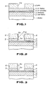
- Fig.1 is a schematic cross-sectional view showing the state in which a resist mask has been formed on an n + -GaAs layer in a typical process in which the present invention is applied to formation of a gate recess in HEMT.
- Fig.2 is a schematic cross-sectional view showing the state in which the n + -GaAs layer of Fig.1 is etched with formation of a sidewall protection film to form the gate recess.
- Fig.3 is a schematic cross-sectional view showing the state in which the sidewall protection film shown in Fig.2 has been removed.
- an n + -GaAs layer on an n + - AlGaAs layer was selectively etched, using an S 2 F 2 /Xe mixed gas to form a recess before forming a gate electrode. This process is explained by referring to Figs.1 to 5.
- a wafer used in the present Example as an etching sample was made up of an epi-GaAs layer 2, grown about 500 nm thick on a semiinsulating GaAs substrate 1, functioning as a buffer layer, an AlGaAs layer 3, about 2 nm thick, an n + -AlGaAs layer 4, about 30 nm thick, doped with n-type impurities, such as Si, an n + -GaAs layer 5, about 100 nm thick, similarly containing n-type impurities, and a resist mask (PR) patterned to a predetermined shape, stacked together in this order, as shown in Fig.1.
- the resist mask 6 was patterned by light exposure by an electron beam lithography method and development, with the diameter of an opening 6a being about 300 nm.
- the wafer was set on an RF bias type magnetic microwave plasma etching device. Etching was carried out under typical etching conditions of an S 2 F 2 flow rate of 20 SCCM, an Xe flow rate of 50 SCCM, a gas pressure of 1.3 Pa (10 mTorr), a microwave power of 850 W (2.45 GHz) and an RF bias power of 100 W (2 MHz).
- etching proceeded anisotropically to form a recess 5a having a vertically extending wall.
- AlF X x being mainly 3
- AlF X may function as an etching mask even under conditions that GaF X was sputtered off, as may be surmised from the fact that AlF 3 has a melting point of 1291°C which is higher than the boiling point of GaF 3 which is about 1000°C.
- the sidewall protecting film 7 could be readily sublimed off, as shown in Fig.3, by heating the wafer to about 90°C after the end of etching, without causing pollution by particles on the wafer.
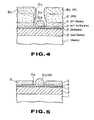
- An layer about 200 nm thick was formed by electron beam deposition, as an example.
- This Al deposition was carried out by intentionally utilizing the fact that step coverage was deteriorated within recess 5a having an extremely small opening diameter.
- an upper Al layer 8a was formed on the surface of the resist mask 6 and a lower Al layer 8b which later become a gate electrode was formed on the bottom of the recess 5a, as shown in Fig.4.
- the upper Al layer 8a was simultaneously removed, as shown in Fig.5, so that only the lower Al layer 8b was left on the bottom of the recess 5a so as to be used as gate electrode.
- the n + -GaAs layer on the n + -AlGaAs layer was selectively etched, using an S 2 F 2 /Cl 2 mixed gas, for etching a gate recess for HEMT.
- the wafer used in Fig.1 was used in the present Example, as in the following Examples.
- This wafer was set on a wafer setting electrode of an RF bias type magnetic microwave plasma etching device.
- An alcoholic coolant medium was supplied from e.g. a chiller mounted outside the device to a cooling pipe enclosed in the wafer setting electrode for cooling the wafer.
- the n + -GaAs layer 5 was etched under typical etching conditions of an S 2 F 2 flow rate of 25 SCCM, a Cl 2 flow rate of 15 SCCM, a gas pressure of 1.3 Pa (10 mTorr), a microwave power of 850 W (2.45 GHz), an RF bias power of 20 W (2 MHz) and a wafer temperature of -10°C.
- the above etching gas composition was equivalent to the composition of Example 2 admixed with H 2 S. Since H 2 S captured F* or Cl* in the etching gas reaction system by H* yielded on its dissociation, while also supplying S, it had a significant effect in raising the apparent S/X ratio in the system. That is, since the sidewall protecting effect was augmented, good anisotropy was realized even although the RF bias power was additionally decreased.
- the over-etching was then carried out under typical conditions of an S 2 F 2 flow rate of 25 SCCM, a Cl 2 flow rate of 15 SCCM, an H 2 S flow rate of 10 SCCM, a gas pressure of 1.3 Pa (10 mTorr), a microwave power of 850 W (2.45 GHz), an RF bias power of 10 W (2 MHz) and a wafer temperature of -10°C.
- the n + -GaAs layer was etched using an S 2 F 2 /S 2 Cl 2 mixed gas under typical etching conditions of an S 2 F 2 flow rate of 20 SCCM, a S 2 Cl 2 flow rate of 20 SCCM, a gas pressure of 1.3 Pa (10 mTorr), a microwave power of 850 W (2.45 GHz), an RF bias power of 20 W (2 MHz) and a wafer temperature of -10°C.
- S 2 Cl 2 is among sulfur chlorides previously proposed by the present inventor as an etching gas for etching a layer of a silicon-based material or an Al-containing material.
- the etching mechanism in the present embodiment was similar to that of Example 2, the sidewall protecting effect was additionally improved because both S 2 F 2 and S 2 Cl 2 served as a supply source for S.
- the over-etching was carried out by altering the conditions typically as an S 2 F 2 flow rate 30 SCCM (proportion, 75%), an S 2 Br 2 flow rate of 10 SCCM, a gas pressure of 1.3 Pa (10 mTorr), a microwave power of 850 W (2.45 GHz), an RF bias power of 10 W (2 MHz) and a wafer temperature of -10°C.
- the selectivity ratio was raised to about 60 because more F* radicals were produced than Br* to promote generation of AlF X and the RF bias power was lowered to diminish the ion incident energy.
- the n + -GaAs layer was etched using an S 2 F 2 /S 2 Cl 2/ Cl 2 mixed gas under just-etching conditions of an S 2 F 2 flow rate of 20 SCCM, an S 2 Cl 2 flow rate of 20 SCCM, a Cl 2 flow rate of 5 SCCM, a gas pressure of 1.3 Pa (10 mTorr), a microwave power of 850 W (2.45 GHz), an RF bias power of 20 W (2 MHz) and a wafer temperature of -10°C (with use of an alcoholic coolant).
- Similar etching was carried out using an S 2 F 2 /S 2 Br 2 /Cl 2 mixed gas under etching conditions of an S 2 F 2 flow rate of 20 SCCM, an S 2 Br 2 flow rate of 15 SCCM, a Cl 2 flow rate of 5 SCCM, a gas pressure of 1.3 Pa (10 mTorr), a microwave power of 850 W (2.45 GHz), an RF bias power of 20 W (2 MHz) and a wafer temperature of -10°C.
- etching gas composition was the same as that of Example 8 except substituting S 2 Br 2 for S 2 Cl 2 of Example 8, and etching proceeded by substantially the same mechanism as that of Example 8 except that bromides were also formed as a reaction product.
- the underlayer selectivity of the present Example was about 30.
- the n + -GaAs layer was just-etched, using an S 2 F 2 /S 2 Cl 2 /Cl 2 mixed gas under just-etching conditions of an S 2 F 2 flow rate of 20 SCCM, an S 2 Cl 2 flow rate of 15 SCCM, a Cl 2 flow rate of 5 SCCM, a gas pressure of 1.3 Pa (10 mTorr), a microwave power of 850 W (2.45 GHz), an RF bias power of 20 W (2 MHz) and a wafer temperature of -10°C (with use of an alcoholic cooling agent), after which an over-etching step was carried out using an S 2 F 2 /S 2 Cl 2 mixed gas under a lower RF bias power condition.
- the over-etching was carried out for removing the residual n + -GaAs layer 5 under typical etching conditions of an S 2 F 2 flow rate of 25 SCCM, an S 2 Cl 2 flow rate of 15 SCCM, a gas pressure of 1.3 Pa (10 mTorr), a microwave power of 850 W (2.45 GHz), an RF bias power of 10 W (2 MHz) and a wafer temperature of -10°C.
- the quantity of Cl* and that of S yielded during this over-etching process are compared to those in the just-etching process by simple calculation from the number of F atoms or S atoms in a molecule and by disregarding the discharge dissociation efficiency of the individual compounds and the recombination of chemical species. It is seen from this comparison that, under the above-mentioned over-etching conditions, the amount of Cl* was diminished by 25% and the amount of S was increased by 10% or more from those under the just-etching conditions, while the RF bias power was also halved.
- SF 6 contains S atoms in its molecule and scarcely releases free S even under discharge dissociation conditions, as experimentally confirmed by the present inventor.
- a large quantity of F* yielded from SF 6 were combined with part of free S so that the sidewall protecting film 7 was formed with a minimum thickness necessary to maintain the anisotropic shape without producing dimensional loss with respect to the resist mask 6. Since F* of the etching reaction system were increased, AlF X was formed with high efficiency on an exposed surface of the underlying n + -AlGaAs layer 4 as soon as the layer 4 was exposed, so that high underlayer selectivity could be achieved.
- the recess 5a having a good anisotropic shape was formed and a selectivity ratio of about 30 with respect to the underlayer of the n + -AlGaAs layer 4 could be achieved.
- the n + -GaAs layer was just-etched using an S 2 F 2 /S 2 Cl 2 /SF 6 mixed gas under just-etching conditions of an S 2 F 2 flow rate of 20 SCCM, an S 2 Cl 2 flow rate of 15 SCCM, an SF 6 flow rate of 5 SCCM, a gas pressure of 1.3 Pa (10 mTorr), a microwave power of 850 W (2.45 GHz), an RF bias power of 20 W (2 MHz) and a wafer temperature of -10°C (with use of an alcoholic coolant), after which an over-etching step was carried out using an S 2 F 2 /S 2 Cl 2 mixed gas under a lower RF bias power condition.
- an overetching was carried out by changing over to typical operating conditions of an S 2 F 2 flow rate of 25 SCCM, an S 2 Cl 2 flow rate of 15 SCCM, a gas pressure of 1.3 Pa (10 mTorr), a microwave power of 850 W (2.45 GHz), an RF bias power of 10 W (2 MHz) and a wafer temperature of -10°C.
- S 3 Cl 2 or SCl 2 may also be employed as depositable chlorine compounds, besides S 2 Cl 2 .
- S 3 Br 2 or SBr 2 may also be employed besides S 2 Br 2 .
- BCl 3 or HCl may also be employed besides Cl 2 .
- Non-depositable bromine compounds give substantially the same results as those of non-depositable chlorine compounds. Although not recited concretely in the Examples, Br 2 , BBr 3 or HBr may also be employed.
- the present invention may be applied to processes in need of selective etching of a stacked system of an Al-free compound semiconductor/Al-containing compound semiconductor other than the above-described process for producing HEMT, such as the process of fabrication of laser devices or quantum Hall devices.
- the etching devices, etching conditions or the wafer constitution may naturally be changed as desired.
Landscapes
- Drying Of Semiconductors (AREA)
- Junction Field-Effect Transistors (AREA)
Claims (5)
- Procédé de gravure à sec pour la gravure sélective à plasma d'une couche semi-conductrice de composé sans Al soit de GaAs, InP, GaN soit InAs empilée sur sa couche semi-conductrice de composé correspondant contenant de l'Al, caractérisé par la
réalisation de la gravure à une température de surface de plaquette inférieure à environ 90°C en utilisant un gaz de gravure contenant au moins un composé de chlore sélectionné à partir du groupe se composant de S2Cl2, S3Cl2, SCl2 ou au moins un composé de brome sélectionné à partir du groupe se composant de S2Br2, S3Br2 et SBr2, et au moins un composé de fluor non déposable sélectionné à partir du groupe se composant de SF6, NF3, XeF2, HF, ClF, ClF3, BrF3 et BrF5. - Procédé de gravure à sec selon la revendication 1, dans lequel ladite couche semi-conductrice de composé contenant de l'Al est une couche d'AlGaAs, ladite couche semi-conductrice de composé sans Al est une couche de GaAs, ledit composé de chlore est du S2Cl2, et ledit composé de fluor non-déposable est du ClF3.
- Procédé de gravure à sec selon la revendication 1, dans lequel gaz de gravure contient en outre au moins du H2 ou du H2S.
- Procédé de gravure à sec selon la revendication 1, comprenant en outreune étape de "gravure juste" de gravure de ladite couche semi-conductrice de composé sans Al dans une quantité correspondant substantiellement à son épaisseur en utilisant ledit gaz de gravure, etune étape de sur-gravure de gravure d'une partie restante de ladite couche semi-conductrice à composé sans Al utilisant ledit gaz de gravure mélangé avec au moins avec un de H2 ou de H2S.
- Procédé de gravure à sec selon la revendication 4, dans lequel ladite étape de sur-gravure de gravure d'une partie restante de ladite couche semi-conductrice à composé sans Al est réalisée dans les conditions d'énergie ionique incidente inférieure à celle dans ladite étape de "gravure juste".
Applications Claiming Priority (16)
| Application Number | Priority Date | Filing Date | Title |
|---|---|---|---|
| JP308327/91 | 1991-10-29 | ||
| JP30832791 | 1991-10-29 | ||
| JP30832791 | 1991-10-29 | ||
| JP32461891 | 1991-12-09 | ||
| JP324618/91 | 1991-12-09 | ||
| JP32461991 | 1991-12-09 | ||
| JP32461991 | 1991-12-09 | ||
| JP32461891 | 1991-12-09 | ||
| JP324619/91 | 1991-12-09 | ||
| JP35969191 | 1991-12-11 | ||
| JP359691/91 | 1991-12-11 | ||
| JP35969191 | 1991-12-11 | ||
| JP215221/92 | 1992-08-12 | ||
| JP21522192 | 1992-08-12 | ||
| JP21522192A JP3298161B2 (ja) | 1991-10-29 | 1992-08-12 | ドライエッチング方法 |
| EP92118456A EP0539963B1 (fr) | 1991-10-29 | 1992-10-28 | Attaque sèche de GaAs |
Related Parent Applications (2)
| Application Number | Title | Priority Date | Filing Date |
|---|---|---|---|
| EP92118456A Division EP0539963B1 (fr) | 1991-10-29 | 1992-10-28 | Attaque sèche de GaAs |
| EP92118456.0 Division | 1992-10-28 |
Publications (3)
| Publication Number | Publication Date |
|---|---|
| EP0731499A2 EP0731499A2 (fr) | 1996-09-11 |
| EP0731499A3 EP0731499A3 (fr) | 1996-11-06 |
| EP0731499B1 true EP0731499B1 (fr) | 1999-08-04 |
Family
ID=27529598
Family Applications (2)
| Application Number | Title | Priority Date | Filing Date |
|---|---|---|---|
| EP96106836A Expired - Lifetime EP0731499B1 (fr) | 1991-10-29 | 1992-10-28 | Procédé de gravure sèche pour GaAs |
| EP92118456A Expired - Lifetime EP0539963B1 (fr) | 1991-10-29 | 1992-10-28 | Attaque sèche de GaAs |
Family Applications After (1)
| Application Number | Title | Priority Date | Filing Date |
|---|---|---|---|
| EP92118456A Expired - Lifetime EP0539963B1 (fr) | 1991-10-29 | 1992-10-28 | Attaque sèche de GaAs |
Country Status (4)
| Country | Link |
|---|---|
| US (1) | US5370769A (fr) |
| EP (2) | EP0731499B1 (fr) |
| JP (1) | JP3298161B2 (fr) |
| DE (2) | DE69225190T2 (fr) |
Families Citing this family (12)
| Publication number | Priority date | Publication date | Assignee | Title |
|---|---|---|---|---|
| JPH06232099A (ja) | 1992-09-10 | 1994-08-19 | Mitsubishi Electric Corp | 半導体装置の製造方法,半導体装置の製造装置,半導体レーザの製造方法,量子細線構造の製造方法,及び結晶成長方法 |
| GB2299894B (en) * | 1992-09-10 | 1997-01-22 | Mitsubishi Electric Corp | Method for producing a semiconductor laser device |
| JPH06314668A (ja) * | 1993-04-30 | 1994-11-08 | Fujitsu Ltd | プラズマエッチング方法及びプラズマエッチング装置 |
| US6808647B1 (en) * | 1999-07-12 | 2004-10-26 | Applied Materials Inc | Methodologies to reduce process sensitivity to the chamber condition |
| US6942816B2 (en) * | 2003-02-12 | 2005-09-13 | Lam Research Corporation | Methods of reducing photoresist distortion while etching in a plasma processing system |
| CN101479858B (zh) * | 2006-05-01 | 2011-05-11 | 三菱化学株式会社 | 集成型半导体发光装置及其制造方法 |
| JP4999400B2 (ja) * | 2006-08-09 | 2012-08-15 | キヤノン株式会社 | 酸化物半導体膜のドライエッチング方法 |
| EP2306497B1 (fr) * | 2009-10-02 | 2012-06-06 | Imec | Procédé de fabrication d'une interface présentant peu de défauts entre un diélectrique et un composé III/V |
| FR3000602B1 (fr) * | 2012-12-28 | 2016-06-24 | Commissariat A L Energie Atomique Et Aux Energies Alternatives | Procede de gravure d'un materiau dielectrique poreux |
| WO2015187227A2 (fr) * | 2014-03-13 | 2015-12-10 | Duke University | Plate-forme électronique pour la détection et la commande de réactions électrochimiques |
| CN114242583B (zh) * | 2021-12-22 | 2023-03-21 | 江苏第三代半导体研究院有限公司 | AlGaN材料的刻蚀方法及其应用 |
| CN117936403B (zh) * | 2023-12-26 | 2024-09-20 | 苏州汉骅半导体有限公司 | 一种GaN HEMT外延材料霍尔测试样品及其制备方法 |
Family Cites Families (2)
| Publication number | Priority date | Publication date | Assignee | Title |
|---|---|---|---|---|
| JPH0336723A (ja) * | 1989-07-04 | 1991-02-18 | Fujitsu Ltd | 半導体装置の製造方法及び電子サイクロトロン共鳴エッチング装置 |
| JPH04221825A (ja) * | 1990-12-24 | 1992-08-12 | Nec Corp | 選択ドライエッチング方法 |
-
1992
- 1992-08-12 JP JP21522192A patent/JP3298161B2/ja not_active Expired - Fee Related
- 1992-10-26 US US07/966,531 patent/US5370769A/en not_active Expired - Fee Related
- 1992-10-28 EP EP96106836A patent/EP0731499B1/fr not_active Expired - Lifetime
- 1992-10-28 DE DE69225190T patent/DE69225190T2/de not_active Expired - Fee Related
- 1992-10-28 DE DE69229749T patent/DE69229749T2/de not_active Expired - Fee Related
- 1992-10-28 EP EP92118456A patent/EP0539963B1/fr not_active Expired - Lifetime
Also Published As
| Publication number | Publication date |
|---|---|
| DE69225190D1 (de) | 1998-05-28 |
| JPH05308063A (ja) | 1993-11-19 |
| EP0539963B1 (fr) | 1998-04-22 |
| EP0731499A3 (fr) | 1996-11-06 |
| DE69225190T2 (de) | 1998-12-03 |
| DE69229749D1 (de) | 1999-09-09 |
| JP3298161B2 (ja) | 2002-07-02 |
| EP0539963A2 (fr) | 1993-05-05 |
| EP0539963A3 (en) | 1993-06-30 |
| US5370769A (en) | 1994-12-06 |
| DE69229749T2 (de) | 2000-01-13 |
| EP0731499A2 (fr) | 1996-09-11 |
Similar Documents
| Publication | Publication Date | Title |
|---|---|---|
| US6287978B1 (en) | Method of etching a substrate | |
| US4726879A (en) | RIE process for etching silicon isolation trenches and polycides with vertical surfaces | |
| US5007982A (en) | Reactive ion etching of silicon with hydrogen bromide | |
| EP0731499B1 (fr) | Procédé de gravure sèche pour GaAs | |
| US20040038537A1 (en) | Method of preventing or suppressing sidewall buckling of mask structures used to etch feature sizes smaller than 50nm | |
| US5354421A (en) | Dry etching method | |
| JP2002517895A (ja) | 高アスペクト比の孔を形成する方法 | |
| EP0820093A1 (fr) | Gravure d'une couche antiréfléchissante organique d'un substrat | |
| EP0555858B1 (fr) | Méthode d'attaque sèche d'un polycide n'utilisant pas de gaz CFC | |
| US5419809A (en) | Dry etching method | |
| JP3186264B2 (ja) | ドライエッチング方法 | |
| JP3282243B2 (ja) | ドライエッチング方法 | |
| JP3331819B2 (ja) | 化合物半導体のプラズマエッチング方法 | |
| JP3250269B2 (ja) | ドライエッチング方法 | |
| JPH07335624A (ja) | ドライエッチング方法 | |
| JP3298226B2 (ja) | ドライエッチング方法 | |
| JP3662275B2 (ja) | ドライエッチング方法 | |
| JPH05166764A (ja) | ドライエッチング方法 | |
| JPH06224158A (ja) | ドライエッチング方法 | |
| JP3246145B2 (ja) | ドライエッチング方法 | |
| JPH05166766A (ja) | ドライエッチング方法 | |
| Lee | Comparison of high-density electron cyclotron resonance and inductively coupled plasma sources for etching of electronic materials: New plasma etch regimes for electronic materials | |
| Humphreys et al. | The application of high density plasma sources for optoelectronic devicefabrication | |
| JPH05166765A (ja) | ドライエッチング方法 | |
| JPH05144784A (ja) | ドライエツチング方法 |
Legal Events
| Date | Code | Title | Description |
|---|---|---|---|
| PUAI | Public reference made under article 153(3) epc to a published international application that has entered the european phase |
Free format text: ORIGINAL CODE: 0009012 |
|
| AC | Divisional application: reference to earlier application |
Ref document number: 539963 Country of ref document: EP |
|
| AK | Designated contracting states |
Kind code of ref document: A2 Designated state(s): DE FR NL |
|
| PUAL | Search report despatched |
Free format text: ORIGINAL CODE: 0009013 |
|
| AK | Designated contracting states |
Kind code of ref document: A3 Designated state(s): DE FR NL |
|
| 17P | Request for examination filed |
Effective date: 19970404 |
|
| GRAG | Despatch of communication of intention to grant |
Free format text: ORIGINAL CODE: EPIDOS AGRA |
|
| 17Q | First examination report despatched |
Effective date: 19980707 |
|
| GRAG | Despatch of communication of intention to grant |
Free format text: ORIGINAL CODE: EPIDOS AGRA |
|
| GRAH | Despatch of communication of intention to grant a patent |
Free format text: ORIGINAL CODE: EPIDOS IGRA |
|
| GRAH | Despatch of communication of intention to grant a patent |
Free format text: ORIGINAL CODE: EPIDOS IGRA |
|
| GRAH | Despatch of communication of intention to grant a patent |
Free format text: ORIGINAL CODE: EPIDOS IGRA |
|
| GRAA | (expected) grant |
Free format text: ORIGINAL CODE: 0009210 |
|
| AC | Divisional application: reference to earlier application |
Ref document number: 539963 Country of ref document: EP |
|
| AK | Designated contracting states |
Kind code of ref document: B1 Designated state(s): DE FR NL |
|
| REF | Corresponds to: |
Ref document number: 69229749 Country of ref document: DE Date of ref document: 19990909 |
|
| ET | Fr: translation filed | ||
| PLBE | No opposition filed within time limit |
Free format text: ORIGINAL CODE: 0009261 |
|
| STAA | Information on the status of an ep patent application or granted ep patent |
Free format text: STATUS: NO OPPOSITION FILED WITHIN TIME LIMIT |
|
| 26N | No opposition filed | ||
| PGFP | Annual fee paid to national office [announced via postgrant information from national office to epo] |
Ref country code: FR Payment date: 20011010 Year of fee payment: 10 |
|
| PGFP | Annual fee paid to national office [announced via postgrant information from national office to epo] |
Ref country code: NL Payment date: 20011031 Year of fee payment: 10 |
|
| PGFP | Annual fee paid to national office [announced via postgrant information from national office to epo] |
Ref country code: DE Payment date: 20011112 Year of fee payment: 10 |
|
| PG25 | Lapsed in a contracting state [announced via postgrant information from national office to epo] |
Ref country code: NL Free format text: LAPSE BECAUSE OF NON-PAYMENT OF DUE FEES Effective date: 20030501 Ref country code: DE Free format text: LAPSE BECAUSE OF NON-PAYMENT OF DUE FEES Effective date: 20030501 |
|
| PG25 | Lapsed in a contracting state [announced via postgrant information from national office to epo] |
Ref country code: FR Free format text: LAPSE BECAUSE OF NON-PAYMENT OF DUE FEES Effective date: 20030630 |
|
| NLV4 | Nl: lapsed or anulled due to non-payment of the annual fee |
Effective date: 20030501 |
|
| REG | Reference to a national code |
Ref country code: FR Ref legal event code: ST |