EP0734072A2 - Dispositif semi-conducteur à grille isolée et son procédé de fabrication - Google Patents
Dispositif semi-conducteur à grille isolée et son procédé de fabrication Download PDFInfo
- Publication number
- EP0734072A2 EP0734072A2 EP96103289A EP96103289A EP0734072A2 EP 0734072 A2 EP0734072 A2 EP 0734072A2 EP 96103289 A EP96103289 A EP 96103289A EP 96103289 A EP96103289 A EP 96103289A EP 0734072 A2 EP0734072 A2 EP 0734072A2
- Authority
- EP
- European Patent Office
- Prior art keywords
- gate structure
- layer
- gate
- dopant
- dielectric material
- Prior art date
- Legal status (The legal status is an assumption and is not a legal conclusion. Google has not performed a legal analysis and makes no representation as to the accuracy of the status listed.)
- Withdrawn
Links
Images


Classifications
-
- H—ELECTRICITY
- H10—SEMICONDUCTOR DEVICES; ELECTRIC SOLID-STATE DEVICES NOT OTHERWISE PROVIDED FOR
- H10D—INORGANIC ELECTRIC SEMICONDUCTOR DEVICES
- H10D12/00—Bipolar devices controlled by the field effect, e.g. insulated-gate bipolar transistors [IGBT]
-
- H—ELECTRICITY
- H10—SEMICONDUCTOR DEVICES; ELECTRIC SOLID-STATE DEVICES NOT OTHERWISE PROVIDED FOR
- H10D—INORGANIC ELECTRIC SEMICONDUCTOR DEVICES
- H10D64/00—Electrodes of devices having potential barriers
- H10D64/60—Electrodes characterised by their materials
- H10D64/66—Electrodes having a conductor capacitively coupled to a semiconductor by an insulator, e.g. MIS electrodes
- H10D64/671—Electrodes having a conductor capacitively coupled to a semiconductor by an insulator, e.g. MIS electrodes the conductor having lateral variation in doping or structure
-
- H—ELECTRICITY
- H10—SEMICONDUCTOR DEVICES; ELECTRIC SOLID-STATE DEVICES NOT OTHERWISE PROVIDED FOR
- H10D—INORGANIC ELECTRIC SEMICONDUCTOR DEVICES
- H10D30/00—Field-effect transistors [FET]
- H10D30/01—Manufacture or treatment
- H10D30/021—Manufacture or treatment of FETs having insulated gates [IGFET]
- H10D30/0221—Manufacture or treatment of FETs having insulated gates [IGFET] having asymmetry in the channel direction, e.g. lateral high-voltage MISFETs having drain offset region or extended-drain MOSFETs [EDMOS]
-
- H—ELECTRICITY
- H10—SEMICONDUCTOR DEVICES; ELECTRIC SOLID-STATE DEVICES NOT OTHERWISE PROVIDED FOR
- H10D—INORGANIC ELECTRIC SEMICONDUCTOR DEVICES
- H10D30/00—Field-effect transistors [FET]
- H10D30/60—Insulated-gate field-effect transistors [IGFET]
- H10D30/601—Insulated-gate field-effect transistors [IGFET] having lightly-doped drain or source extensions, e.g. LDD IGFETs or DDD IGFETs
- H10D30/603—Insulated-gate field-effect transistors [IGFET] having lightly-doped drain or source extensions, e.g. LDD IGFETs or DDD IGFETs having asymmetry in the channel direction, e.g. lateral high-voltage MISFETs having drain offset region or extended drain IGFETs [EDMOS]
-
- H—ELECTRICITY
- H10—SEMICONDUCTOR DEVICES; ELECTRIC SOLID-STATE DEVICES NOT OTHERWISE PROVIDED FOR
- H10D—INORGANIC ELECTRIC SEMICONDUCTOR DEVICES
- H10D62/00—Semiconductor bodies, or regions thereof, of devices having potential barriers
- H10D62/10—Shapes, relative sizes or dispositions of the regions of the semiconductor bodies; Shapes of the semiconductor bodies
- H10D62/17—Semiconductor regions connected to electrodes not carrying current to be rectified, amplified or switched, e.g. channel regions
- H10D62/351—Substrate regions of field-effect devices
- H10D62/357—Substrate regions of field-effect devices of FETs
- H10D62/364—Substrate regions of field-effect devices of FETs of IGFETs
- H10D62/371—Inactive supplementary semiconductor regions, e.g. for preventing punch-through, improving capacity effect or leakage current
-
- H—ELECTRICITY
- H10—SEMICONDUCTOR DEVICES; ELECTRIC SOLID-STATE DEVICES NOT OTHERWISE PROVIDED FOR
- H10D—INORGANIC ELECTRIC SEMICONDUCTOR DEVICES
- H10D64/00—Electrodes of devices having potential barriers
- H10D64/20—Electrodes characterised by their shapes, relative sizes or dispositions
- H10D64/27—Electrodes not carrying the current to be rectified, amplified, oscillated or switched, e.g. gates
- H10D64/311—Gate electrodes for field-effect devices
- H10D64/411—Gate electrodes for field-effect devices for FETs
- H10D64/511—Gate electrodes for field-effect devices for FETs for IGFETs
- H10D64/517—Gate electrodes for field-effect devices for FETs for IGFETs characterised by the conducting layers
- H10D64/518—Gate electrodes for field-effect devices for FETs for IGFETs characterised by the conducting layers characterised by their lengths or sectional shapes
-
- H—ELECTRICITY
- H10—SEMICONDUCTOR DEVICES; ELECTRIC SOLID-STATE DEVICES NOT OTHERWISE PROVIDED FOR
- H10D—INORGANIC ELECTRIC SEMICONDUCTOR DEVICES
- H10D64/00—Electrodes of devices having potential barriers
- H10D64/60—Electrodes characterised by their materials
- H10D64/66—Electrodes having a conductor capacitively coupled to a semiconductor by an insulator, e.g. MIS electrodes
- H10D64/675—Gate sidewall spacers
- H10D64/679—Gate sidewall spacers comprising air gaps
-
- H—ELECTRICITY
- H10—SEMICONDUCTOR DEVICES; ELECTRIC SOLID-STATE DEVICES NOT OTHERWISE PROVIDED FOR
- H10D—INORGANIC ELECTRIC SEMICONDUCTOR DEVICES
- H10D84/00—Integrated devices formed in or on semiconductor substrates that comprise only semiconducting layers, e.g. on Si wafers or on GaAs-on-Si wafers
- H10D84/01—Manufacture or treatment
- H10D84/0123—Integrating together multiple components covered by H10D12/00 or H10D30/00, e.g. integrating multiple IGBTs
- H10D84/0126—Integrating together multiple components covered by H10D12/00 or H10D30/00, e.g. integrating multiple IGBTs the components including insulated gates, e.g. IGFETs
- H10D84/0165—Integrating together multiple components covered by H10D12/00 or H10D30/00, e.g. integrating multiple IGBTs the components including insulated gates, e.g. IGFETs the components including complementary IGFETs, e.g. CMOS devices
- H10D84/0181—Manufacturing their gate insulating layers
-
- H—ELECTRICITY
- H10—SEMICONDUCTOR DEVICES; ELECTRIC SOLID-STATE DEVICES NOT OTHERWISE PROVIDED FOR
- H10D—INORGANIC ELECTRIC SEMICONDUCTOR DEVICES
- H10D84/00—Integrated devices formed in or on semiconductor substrates that comprise only semiconducting layers, e.g. on Si wafers or on GaAs-on-Si wafers
- H10D84/01—Manufacture or treatment
- H10D84/02—Manufacture or treatment characterised by using material-based technologies
- H10D84/03—Manufacture or treatment characterised by using material-based technologies using Group IV technology, e.g. silicon technology or silicon-carbide [SiC] technology
- H10D84/038—Manufacture or treatment characterised by using material-based technologies using Group IV technology, e.g. silicon technology or silicon-carbide [SiC] technology using silicon technology, e.g. SiGe
Definitions
- the present invention relates, in general, to insulated gate semiconductor devices, and more particularly, to controlling a threshold voltage, V T , and increasing a transconductance, g m , of insulated gate semiconductor devices.
- V T is related to the voltage at which an insulated gate semiconductor device turns on and varies in accordance with the carrier concentration of the channel region.
- V GS gate-source voltage
- the gate-source voltage (V GS ) of an N-channel insulated gate semiconductor device must exceed V T to form a channel in the insulated gate semiconductor device.
- the voltage at the gate is typically the input voltage of the insulated gate semiconductor device, the input voltage relative to the source voltage must exceed V T for a conducting channel to be formed.
- I D drain current
- V T is important in determining the saturation current of an insulated gate semiconductor device, which in turn helps determine the power bandwidth of the device.
- V T Although precise control of V T is highly desirable in all insulated gate semiconductor device applications, it is particularly important in low voltage applications.
- the difference between the upper power supply rail (5 volts) and the lower power supply rail (0 volts) is sufficiently large, i.e., approximately 5 volts, that fluctuations in V T have a negligible effect on the device performance.
- V T represents a substantial portion of the total power supply voltage. Consequently, fluctuations in V T result in large fluctuations of the current drive capability of the insulated gate semiconductor device.
- the transconductance, g m of the insulated gate field effect transistors is influenced by their V GS , I D , and V T . Since the transconductance increases as I D increases, it is desirable to maximize I D , thereby increasing the transconductance. Further, a high frequency switching speed of the insulated gate field effect transistors is reduced by the combination of the gate to drain capacitance and the gate to source capacitances, collectively referred to as gate capacitances. Thus, a large gate capacitance lowers decreases the bandwidth or lowers the frequency response of the insulated gate field effect transistor.
- an insulated gate field effect transistor and method of manufacturing the insulated gate field effect transistor that provides control of the threshold voltage and minimization of the gate capacitance in low voltage, high bandwidth applications.
- the present invention provides an insulated gate semiconductor device and a method of fabricating or forming the insulated gate semiconductor device.
- Insulated gate semiconductor devices are also referred to as insulated gate field effect devices and insulated gate field effect transistors.
- the insulated gate semiconductor devices manufactured in accordance with the present invention have a reduced gate capacitance, thus a higher frequency response or bandwidth, compared to insulated gate semiconductor devices manufactured by other methods.
- the insulated gate semiconductor devices of the present invention have a lightly doped drain (LDD) extension at a drain region of the device which permits formation of a thicker gate dielectric material between the portion of the gate structure adjacent the drain region and the lightly doped drain extension region.
- LDD lightly doped drain
- the gate structure comprises two conductive portions: a conductive portion near the drain region of the device which serves as a shunt electrode and an extension, i.e., a second conductive portion, adjacent the source region of the device which serves as an active gate structure.
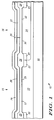
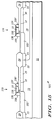
- FIG. 1 illustrates an enlarged cross-sectional view of a portion of partially completed complementary insulated gate field effect transistors 10 during processing in accordance with a first embodiment of the present invention.
- Complementary insulated gate field effect transistors 10 include an N-channel transistor 15 fabricated in a portion of a P-type epitaxial layer 13 and a P-channel transistor 16 fabricated in a portion of an N-well 14.
- a substrate 11 of P conductivity type having an epitaxial layer 13 disposed thereon.
- epitaxial layer 13 is of P conductivity type, has a major surface 12, and ranges in thickness between approximately 2 microns ( ⁇ m) and 5 ⁇ m.
- an impurity well 14 of N conductivity type is formed in a portion of P-type epitaxial layer 13.
- Substrate 11 has, for example, a resistivity ranging from approximately 0.01 ohm-centimeter ( ⁇ -cm) to approximately 0.1 ⁇ -cm, and P-type epitaxial layer 13 has a resistivity between approximately 6 ⁇ -cm and approximately 8 ⁇ -cm.
- P-type epitaxial layer 13 and N-well 14 have a surface concentration on the order of 5 X 10 15 atoms per cubic centimeter (atoms/cm 3 ).
- insulated gate field effect transistors of the present invention may be manufactured in a semiconductor material such as substrate 11.
- field implant regions 22 are formed in P-type epitaxial layer 13
- field implant regions 23 are formed in N-well 14
- field oxide regions 24 are formed over field implant regions 22 and 23. Formation of epitaxial layers, dopant wells, field implant regions, and field oxide regions are well known to those skilled in the art.
- An implant block mask (not shown) such as, for example, photoresist, is formed over N-well 14 and an impurity material of N conductivity type is implanted into a portion of P-type epitaxial layer 13 to form a dopant layer 25 between two adjacent field oxide regions 24.
- dopant layer 25 is shown as extending across an entire portion of P-type epitaxial layer 13 between adjacent field oxide regions 24, it should be understood that dopant layer 25 may be formed to extend across a subportion of the P-type epitaxial layer 13 that is between adjacent field oxide regions 24.
- the implant block mask is removed and an implant block mask is formed on the P-type epitaxial layer 13.
- An impurity material of P conductivity type is implanted into a portion of N-well 14 to form a dopant layer 30 between two adjacent field oxide regions 24. Similar to dopant layer 25, dopant layer 30 may be formed to extend across a subportion of N-well 14. It should be noted that dopant layers 25 and 30 serve as drain extension regions for field effect transistors manufactured in P-type epitaxial layer 13 and N-well 14, respectively. Further, dopant layers 25 and 30 permit the formation of a portion of the gate oxide layer to be sufficiently thick to reduce the gate capacitance, thereby improving the frequency response of the field effect transistors.
- layers 25 and 30 have a surface concentration ranging from approximately 7 x 10 16 atoms/cm 3 to approximately 2 x 10 17 atoms/cm 3 .
- a suitable set of implant conditions to obtain the aforementioned surface concentration includes: an implant dose ranging from approximately 1 x 10 12 atoms per square centimeter (atoms/cm 2 ) to approximately 3 x 10 12 atoms/cm 2 for both layers 25 and 30; an implant energy for forming dopant layer 25 ranging from approximately 50 kilo-electron volts (KeV) to approximately 200 KeV; and an implant energy for forming dopant layer 30 ranging from approximately 25 KeV to approximately 100 KeV.
- KeV kilo-electron volts
- a layer of dielectric material 26 is formed on major surface 12. Although some oxidation procedures increase the thickness of field oxide regions 24 during the formation of oxide layer 26, to simplify the description of the present invention and because the increase in thickness is small relative to the overall thickness of field oxide regions 24, the increase in the thickness of field oxide region 24 is not shown.
- a suitable technique for forming oxide layer 26 is thermal oxidation.
- oxide layer 26 has a thickness of at least 400 angstroms.
- oxide layer 26 has a thickness in the range of approximately 600 angstroms to approximately 1,800 angstroms.
- a typical thickness of oxide layer 26 is approximately 1,200 angstroms. It should be noted that portions of oxide layer 26 serve as portions of a gate oxide for transistors 15 and 16.
- a layer of polysilicon 27 is formed on oxide layer 26 using, for example, a chemical vapor deposition technique.
- a suitable thickness range for polysilicon layer 27 is from approximately 2,500 angstroms to approximately 4,000 angstroms.
- a typical thickness for polysilicon layer 27 is approximately 3,300 angstroms.
- a layer of dielectric material 28 is formed on polysilicon layer 27.
- layer of dielectric material 28 is a layer of oxide formed by the decomposition of tetraethyl orthosilicate (TEOS). Oxide layers formed by the decomposition of tetraethyl orthosilicate are commonly referred to as TEOS layers.
- TEOS tetraethyl orthosilicate
- oxide layer 28 has a thickness ranging from approximately 50 angstroms to approximately 400 angstroms and a nominal thickness of approximately 150 angstroms.
- a layer of silicon nitride 29 is formed on layer of dielectric material 28 using, for example, a low pressure chemical vapor deposition (LPCVD) technique.
- LPCVD low pressure chemical vapor deposition
- a suitable range of thicknesses for silicon nitride layer 29 is between approximately 150 angstroms and approximately 350 angstroms, and nominal thickness for silicon nitride layer 29 is approximately 250 angstroms.
- portions 32 and 33 of the gate structures are formed over a portion of P-type epitaxial layer 13 and over a portion of N-well 14.
- Gate shunt portions 32 and 33 form part of gate structures 61 and 62, respectively, and are shown and further described in FIG. 8. It should be noted that portions 32 and 33 are formed from polysilicon layer 27 and that portion 32 has sides 36 and 37, and a top surface 45, and portion 33 has sides 38 and 39, and a top surface 50.
- Portions 32 and 33 serve as gate shunt portions of gate structures and are formed by anisotropically etching nitride layer 29, oxide layer 28, and polysilicon layer 27.
- Gate shunt portions 32 and 33 may be formed, for example, by coating silicon nitride layer 29 with a layer of photoresist (not shown), exposing the portions of silicon nitride layer 29 to be removed (using, for example, photolithographic techniques), and anisotropically etching the exposed portions of silicon nitride layer 29.
- the portions of oxide layer 28 and polysilicon layer 27 below the exposed portions of silicon nitride layer 29 are also etched, thereby exposing portions of oxide layer 26 and field oxide regions 24.
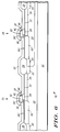
- oxide layer 41 is formed on exposed sides 36, 37, 38, and 39 of the respective gate shunt portions 32 and 33.
- oxide layer 41 is formed by thermally oxidizing the sides 36, 37, 38, and 39.
- a suitable thickness range for oxide layer 41 is between approximately 50 angstroms and approximately 250 angstroms, and a nominal thickness of oxide layer 41 is approximately 100 angstroms.
- a conformal layer of dielectric material 43 is formed on gate shunt portions 32 and 33 as well as on oxide layer 26 and field oxide regions 24.
- layer of dielectric material 43 is silicon nitride having a thickness ranging from approximately 250 angstroms to approximately 750 angstroms, and a nominal thickness of approximately 400 angstroms. It should be noted that the impurity materials of dopant layers 25 and 30 are activated or driven into P-type epitaxial layer 13 and N-well 14, respectively, by the processing steps described supra.
- silicon nitride layer 43 is anisotropically etched to form spacers 46, 46', 47, and 47' adjacent oxide layer 41.
- a suitable technique for etching silicon nitride layer 43 includes a reactive ion etch (RIE) using etchants such as CF 4 , NF 3 , and the like.
- the anisotropic etch step may remove a portion of oxide layer 26.
- oxide layer 26 is thinned to approximately 400 angstroms after the formation of spacers 46, 46', 47, and 47'. It should be noted that spacers 46 and 47 protect portions of oxide layer 26 and that spacers 46' and 47' shape oxide layer 26 in order to create a repeatable undercut etch profile (shown in FIG. 5).
- a layer of photoresist (not shown) is formed on subportions of gate shunt portions 32 and 33 and on spacers 46 and 47.
- Spacers 46' and 47' and the portions of oxide layers 26 and 28 which are not covered by the layer of photoresist are removed via a sequence of isotropic etches, i.e., a first etch step to remove spacers 46' and 47' and a second etch step to remove portions of oxide layer 26 between gate shunt portion 32 and a first portion of major surface 12 as well as the portion of oxide layer 26 between gate shunt portion 33 and a second portion of major surface 12.
- gate shunt portions 32 and 33 are undercut on one side to form a cavity 35 underneath gate shunt portion 32, i.e., between gate shunt portion 32 and the first portion of major surface 12 and a cavity 35' underneath gate shunt portion 33, i.e., between gate shunt portion 33 and the second portion of major surface 12.
- the layer of photoresist is removed.
- a screen oxide 40 is formed on the exposed portions of gate shunt portions 32 and 33, respectively, and on the exposed portions of major surface 12.
- oxide layer 40 has a thickness ranging from approximately 100 angstroms to approximately 200 angstroms, with a nominal thickness of approximately 150 angstroms.
- oxide layer 40 is also formed on field oxide regions 24 and oxide layer 26, it should be noted that to simplify the description of the present invention, these portions of oxide layer 40 are not shown.
- a layer of photoresist (not shown) is formed on portions of oxide 40 disposed on gate shunt portions 32 and 33, spacers 46 and 47, portions of oxide layer 40 adjacent sides 37 and 39, and portions of field oxide regions 24. This layer of photoresist serves as an implant block mask.
- An enhanced dopant region 51 is formed by doping a portion of P-type epitaxial layer 13 with an impurity material of P conductivity type such as, for example, boron. More particularly, the boron is implanted into a portion of P-type epitaxial layer 13 to form dopant region 51. Dopant region 51 is laterally aligned to field oxide region 24 of N-channel transistor 15 and oxide layer 40 disposed on side 36 of gate shunt portion 32. It should be noted that dopant region 51 is spaced apart from major surface 12.
- an impurity material of P conductivity type such as, for example, boron. More particularly, the boron is implanted into a portion of P-type epitaxial layer 13 to form dopant region 51.
- Dopant region 51 is laterally aligned to field oxide region 24 of N-channel transistor 15 and oxide layer 40 disposed on side 36 of gate shunt portion 32. It should be noted that dopant region 51 is spaced apart from major surface 12.
- a suitable set of implant parameters includes implanting the P type impurity material at a dose ranging from approximately 2 x 10 12 atoms/cm 2 to approximately 2 x 10 13 atoms/cm 2 at an implant energy ranging from approximately 40 KeV to approximately 100 KeV.
- the boron that forms dopant region 51 is implanted into P-type epitaxial layer 13 to a depth or distance ranging between approximately 1,500 and approximately 3,000 angstroms.
- the impurity materials or dopant forming dopant region 51 serves to provide punch-through protection for N-channel transistor 15.
- An enhanced dopant region 52 is formed by doping another portion of P-type epitaxial layer 13 with boron.
- implant parameters for the formation of dopant region 52 include a dose ranging from approximately 5 x 10 11 atoms/cm 2 to approximately 1 x 10 13 atoms/cm 2 and a suitable implant energy ranging from approximately 10 KeV to approximately 20 KeV.
- the boron that forms dopant region 52 is implanted into a portion of P-type epitaxial layer 13 to a depth or distance ranging from approximately 200 to approximately 1,200 angstroms.
- the impurity materials forming dopant region 52 serves to adjust the threshold voltage of N-channel transistor 15.
- the layer of photoresist is removed and a layer of photoresist (not shown) is formed on portions of screen oxide 40 disposed on gate shunt portions 32 and 33, spacer 47, portions of oxide layer 26 adjacent spacer 47, portions of oxide layer 26 over P-type epitaxial layer 13, and portions of field oxide regions 24.
- This layer of photoresist also serves as an implant block mask.
- An enhanced dopant region 53 is formed by doping a portion of N-well 14 with an impurity material of N conductivity type such as, for example, phosphorus. More particularly, the phosphorus is implanted into N-well 14 to form dopant region 53. It should be noted that dopant region 53 is spaced apart from surface 12.
- a suitable set of implant parameters includes implanting the N type impurity material at a dose ranging from approximately 2 x 10 12 atoms/cm 2 to approximately 2 x 10 13 atoms/cm 2 at an implant energy ranging from approximately 80 KeV to approximately 200 KeV.
- the N type impurity material of the implant step that forms dopant region 53 is implanted into N-well 14 to a depth or distance ranging from approximately 1,500 to approximately 3,000 angstroms.
- the impurity materials forming dopant region 53 serves to provide punch-through protection for P-channel transistor 16.
- An enhanced dopant region 54 is formed by doping another portion of N-well 14 with phosphorus.
- the boron is implanted into N-well 14 to form dopant region 54.
- Suitable implant parameters for the formation of dopant region 54 include a dose ranging from approximately 5 x 10 11 atoms/cm 2 to approximately 1 x 10 13 atoms/cm 2 and a suitable implant energy ranging from approximately 20 KeV to approximately 40 KeV.
- the N type impurity material of the implant step that forms dopant region 54 is implanted into N-well 14 to a depth or distance ranging from approximately 200 to 1,200 angstroms.
- the impurity materials forming dopant region 54 serves to adjust the threshold voltage of P-channel transistor 16.
- the layer of photoresist is removed.
- screen oxide 40 is removed from gate shunt portions 32 and 33, respectively, and portions of major surface 12, thereby exposing subportions of gate shunt portions 32 and 33 and portions of major surface 12 and forming oxide extensions 55.
- An oxide layer 26' is formed on the exposed portions of major surface 12 and the exposed regions of gate shunt portions 32 and 33.
- a conformal layer of polysilicon 57 having a thickness ranging between approximately 1,000 angstroms and approximately 2,500 angstroms is deposited on oxide layers 24, 26', 41, and on spacers 46 and 47. Nominally, polysilicon layer 57 has a thickness of approximately 1,750 angstroms.
- dopant regions 51 and 52 are initially spaced apart, it should be noted that they diffuse towards each other and form a single dopant region 51'.
- dopant regions 53 and 54 diffuse towards each other and form a single dopant region 53'.
- polysilicon layer 57 is anisotropically etched to form gate extensions 58 and 59 adjacent sides 36 and 38, respectively. It should be noted that gate extensions 58 and 59 are spaced apart from the respective sides 36 and 38 by portions of oxide layer 26'. In addition, extensions 58' and 59' are formed adjacent spacers 46 and 47, respectively.
- the anisotropic etch step that forms gate extensions 58, 58', 59, and 59' stops on or in oxide layer 26'.
- gate structure 61 comprises a gate shunt portion 32 formed from a first polysilicon portion on the oxide layer 26 of a first width and a gate extension portion 58 formed from a second polysilicon portion on a portion of oxide layer 26' of a second width, wherein the second width is less than the first width.
- gate structure 62 comprises a gate shunt portion 33 formed from a polysilicon portion on the oxide layer 26 of the first width and a gate extension portion 59 formed from a another polysilicon portion on a portion of oxide layer 26' of the second width.
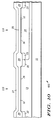
- a layer of photoresist (not shown) is formed on gate shunt portions 32 and 33, gate extensions 58 and 59, and the portions of oxide layer 26' adjacent gate extensions 58 and 59.
- gate extensions 58' and 59' and the portions of oxide layer 26' adjacent gate extensions 58' and 59' are uncovered by photoresist, i.e., they are exposed.
- the layer of photoresist serves as an etch protect mask.
- Gate extensions 58' and 59' and spacers 46 and 47 are removed using, for example, an isotropic plasma etch. Although spacers 46 and 47 are shown as being completely removed, it should be noted that they may be reduced in size. In addition, the exposed portions of oxide layer 26' are also removed. The layer of photoresist is removed.
- gate extension 58 cooperates with gate shunt portion 32 and the portions of oxide layer 26' on P-type epitaxial layer 13 to form a gate structure 61.
- gate extension 59 cooperates with gate shunt portion 33 and a portion of oxide layer 26' on N-well 14 to form gate structure 62.
- the portions of oxide layer 26' between gate extension 58 and major surface 12 and between gate extension 59 and major surface 12 serve as active gate oxide.
- oxide layer 60 is conformally deposited on field oxide regions 24, and the remaining portions of oxide layer 26', oxide layer 41, spacers 46 and 47, and gate extensions 58 and 59.
- oxide layer 60 has a thickness ranging from approximately 100 angstroms to approximately 300 angstroms, wherein a nominal thickness of oxide layer 60 is approximately 150 angstroms.
- a layer of photoresist (not shown) is formed on the portions of the layer of dielectric material 60 over gate structures 61 and 62 and the portions of oxide layer 60 over N-well 14 that are adjacent to gate structure 62.
- the layer of photoresist serves as an implant protect mask preventing P-channel transistor 16 from being doped by a source/drain implant for N-channel transistor 15.
- a source/drain implant is performed to form a source region 63 and a drain region 64.
- the source/drain implant further dopes gate structure 61.
- a suitable set of implant parameters for the source/drain implant includes implanting an N type impurity material such as arsenic, at a dose in the range of approximately 1 x 10 15 atoms/cm 2 to approximately 1 x 10 16 atoms/cm 2 , and a suitable implant energy ranges from approximately 60 KeV to approximately 120 KeV.
- an N type impurity material such as arsenic
- the layer of photoresist is removed and another layer of photoresist (not shown) is formed on the portion of the layer of dielectric material 60 above gate structures 61 and 62 and the portions of oxide layer 60 over P-type epitaxial layer 13 adjacent gate structure 61.
- the layer of photoresist serves as an implant protect mask preventing N-channel transistor 15 from being doped by a source/drain implant of the P-channel transistor 16.
- a source/drain implant of, for example, boron is performed to form a source region 66 and a drain region 67.
- the source/drain implant further dopes gate structure 62.
- a suitable set of implant parameters for the source/drain implant includes implanting a P type impurity material such as boron, at a dose in the range of approximately 1 X 10 15 atoms/cm 2 to approximately 5 X 10 15 atoms/cm 2 , and a suitable implant energy ranges from approximately 5 KeV to approximately 15 KeV.
- the layer of photoresist is removed.
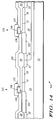
- a conformal layer of dielectric material 69 is formed on layer of dielectric material 60.
- layer of dielectric material 69 is silicon nitride having a thickness ranging from approximately 1,000 angstroms to approximately 2,250 angstroms.
- a nominal thickness of silicon nitride layer 69 is 2,000 angstroms.
- silicon nitride layer 69 and oxide layer 60 are anisotropically etched to form oxide spacers 70 and nitride spacers 71 adjacent sides 36 and 37. Further, oxide spacers 70' and nitride spacers 71' are formed adjacent the remaining portions of spacers 46 and 47. In addition, the anisotropic etch step exposes gate shunt portions 32 and 33 and gate extensions 58 and 59 of gate structures 61 and 62, respectively, as well as the portion of major surface 12 adjacent spacers 71 and 71'.
- a silicide 76 is formed on dopant region 63
- a silicide 77 is formed on dopant region 64
- a silicide 78 is formed on portions of gate structure 61
- a silicide 79 is formed on dopant region 66
- a silicide 81 is formed on dopant region 67
- a silicide 82 on portions of gate structure 62.
- silicide 78 serves as a conductive strap coupling gate shunt portion 32 to gate extension 58
- silicide 82 serves as a conductive strap coupling gate shunt portion 33 to gate extension 59.
- a layer of dielectric material 84 such as, for example, oxide is formed on field oxide regions 24, spacers 71 and 71', and silicide 76, 77, 78, 79, 81, and 82. Openings are formed in oxide layer 84 to expose portions of silicide 76, 77, 78, 79, 81, and 82. Using techniques well known in the art, electrical conductors or electrodes are formed which contact the exposed portions of silicide 76, 77, 78, 79, 81, and 82. More particularly, a source conductor 86 contacts silicide 76, a drain conductor 87 contacts silicide 77, and a gate conductor 88 contacts silicide 78.
- source, drain, and gate conductors, 86, 87, and 88, respectively, form conductors for N-channel transistor 15.
- a source conductor 89 contacts silicide 79
- a drain conductor 91 contacts silicide 81
- a gate conductor 92 contacts silicide 82.
- source, drain, and gate conductors, 89, 91, and 92, respectively, form conductors for P-channel transistor 16.
- gate conductors 88 and 92 are highly simplified illustrations to show a gate conductor electrically coupled to a gate structure.
- FIGs. 10-18 illustrate highly enlarged cross-sectional views of a portion of complementary insulated gate field effect transistors 100 during processing in accordance with a second embodiment of the present invention.
- Complementary insulated gate field effect transistors 100 include an N-channel transistor 115 fabricated in a portion of a P-type epitaxial layer 13 and a P-channel transistor 116 fabricated in a portion of an N-well 14.
- FIG. 10 illustrates the partially completed insulated gate field effect transistor 100 after formation of oxide layer 26 and layer of polysilicon 27. It should be noted that the formation of epitaxial layer 13, N-well 14, field implant regions 22 and 23, field oxide regions 24, dopant regions 25 and 30, oxide layer 26 and polysilicon layer 27 have been described with reference to FIG. 1. It should be understood that the locations of N-channel transistor 115 and P-channel transistor 116 in FIGs. 10-18 are included to show the locations of these structures and therefore more clearly describe the invention.
- gate shunt portions 132 and 133 of the gate structures are formed over P-type epitaxial layer 13 and N-well 14, respectively.
- Gate shunt portion 132 having sides 136 and 137 and gate shunt portion 133 having sides 138 and 139 may be formed by anisotropically etching polysilicon layer 27.
- gate shunt portions 132 and 133 are formed by coating polysilicon layer 27 with a layer of photoresist (not shown), exposing the portions of polysilicon layer 27 to be removed (using photolithographic techniques), and anisotropically etching the exposed portions of polysilicon layer 27.
- gate shunt portions 132 and 133 are formed from portions of polysilicon layer 27. It should be understood that gate shunt portions 132 and 133 form part of gate structures 161 and 162, respectively, which are further described in the description of FIG. 16.
- a layer of oxide 141 is formed on gate shunt portions 132 and 133.
- oxide layer 141 is formed by thermally oxidizing gate shunt portions 132 and 133.
- a suitable thickness range for oxide layer 141 is between approximately 50 angstroms and approximately 250 angstroms and a nominal thickness of oxide layer 141 is approximately 100 angstroms.
- the formation of oxide layer 141 by thermal oxidation increases the thicknesses of field oxide regions 24 and oxide layer 26, the increased thicknesses are not shown to simplify the description of the present invention.
- a layer of photoresist 142 having an opening 143, is formed on oxide layer 141, field oxide regions 24 and oxide layer 26. Opening 143 exposes a sub-portion of gate shunt portion 132 and a portion of oxide layer 26 adjacent side 136 of gate shunt portion 132.
- Layer of photoresist 142 serves as an implant block mask.
- an enhanced dopant region 151 is formed by doping a portion of P-type epitaxial layer 13 with an impurity material of P conductivity type such as, for example, boron. More particularly, the boron is implanted into P-type epitaxial layer 13 to form a dopant region 151. It should be noted that dopant region 151 is spaced apart from surface 12.
- a suitable set of implant parameters for forming dopant region 151 includes implanting the boron at a dose in the range of approximately 2 x 10 12 atoms/cm 2 and approximately 2 x 10 13 atoms/cm 2 and an implant energy ranging between approximately 40 KeV and approximately 100 KeV.
- the boron forming dopant region 151 is implanted into P-type epitaxial layer 13 at a depth or distance ranging from approximately 1,500 to 3,000 angstroms.
- the impurity materials forming dopant region 151 serves to provide punch-through protection for N-channel transistor 115.
- An enhanced dopant region 152 is formed by doping another portion of P-type epitaxial layer 13 with boron.
- another implant is performed wherein the boron is implanted into P-type epitaxial layer 13 to a form dopant region 152.
- Suitable implant parameters for the formation of dopant region 152 include implanting the boron at a dose in the range of approximately 5 x 10 11 atoms/cm 2 and approximately 1 x 10 13 atoms/cm 2 and a suitable implant energy ranging between approximately 10 KeV and approximately 20 KeV.
- the boron forming dopant region 152 is implanted into P-type epitaxial layer 13 to a depth or distance ranging from approximately 200 to approximately 1,200 angstroms and serves to adjust the threshold voltage of N-channel transistor 115.
- the layer of photoresist is removed and a layer of photoresist 144, having an opening 145, is formed on oxide layer 141, field oxide regions 24, and portions of oxide layer 26. Opening 145 exposes a subportion of gate shunt portion 133 and a portion of oxide layer 26 adjacent side 138 of gate shunt portion 133.
- Layer of photoresist 144 serves as an implant block mask.
- an enhanced dopant region 153 is formed by doping a portion of N-well 14 with an impurity material of N conductivity type such as, for example, phosphorus. More particularly, the phosphorus is implanted into N-well 14 to form dopant region 153. It should be noted that dopant region 153 is spaced apart from surface 12.
- a suitable set of implant parameters includes implanting the P type impurity material at a dose in the range of approximately 2 x 10 12 atoms/cm 2 and approximately 2 x 10 13 atoms/cm 2 and an implant energy ranging between approximately 40 KeV and approximately 100 KeV.
- the N type impurity material of the implant step that forms dopant region 153 is implanted into N-well 14 to depth or distance ranging from approximately 1,500 to 3,000 angstroms.
- the implant forming dopant region 153 serves to provide punch-through protection for P-channel transistor 116.
- An enhanced dopant region 154 is formed by doping another portion of N-well 14 with phosphorus.
- another implant is performed wherein the impurity material of N conductivity type is implanted into N-well 14 to form dopant region 154.
- Suitable implant parameters for the formation of dopant region 154 include a dose ranging between approximately 5 x 10 11 atoms/cm 2 and approximately 1 x 10 13 atoms/cm 2 and a suitable implant energy ranging between approximately 20 KeV and approximately 40 KeV.
- the N type impurity material of the implant step that forms dopant region 154 is implanted into N-well 14 to a depth or distance ranging from approximately 200 to approximately 1,200 angstroms.
- the implant forming dopant region 154 serves to adjust the threshold voltage of P-channel transistor 116. Layer of photoresist 144 is removed.
- a layer of photoresist 148 having openings 149, is formed on oxide layer 141. Openings 149 expose a sub-portion of gate shunt portion 132, a portion of oxide layer 26 adjacent side 136 of gate shunt portion 132, a sub-portion of gate shunt portion 133, and a portion of oxide layer 26 adjacent side 138 of gate shunt portion 133.
- Layer of photoresist 148 serves as an etch protect mask.
- the exposed portions of oxide layer 26 and oxide layer 141 are isotropically etched using, for example, a wet hydrofluoric acid etch.
- the isotropic etch removes approximately 1,000 angstroms of the exposed portions of oxide layer 26 and portions of oxide layer 26 beneath gate shunt portions 132 and 133, i.e., portion of major surface 12 between and gate shunt portions 132 and 133.
- the isotropic etch undercuts the portions of oxide layer 26 between major surface 12 and gate shunt portions 132 and 133 and forms cavities 135 and 135', respectively, between gate shunt portion 132 and a first portion of major surface 12 and between gate shunt portion 133 and a second portion of major surface 12.
- the isotropic etch removes the exposed portions of oxide layer 141 from gate shunt portions 132 and 133. Layer of photoresist 148 is removed.
- oxide layer 156 is a thin oxide layer having a thickness ranging between approximately 50 angstroms and approximately 150 angstroms. A nominal thickness of oxide layer 156 is approximately 90 angstroms.
- oxide layer 156 is also formed on field oxide regions 24 and oxide layer 26, it should be noted that oxide layer 156 merely thickens or increases the thicknesses of field oxide regions 24 and oxide layer 26. Thus, to simplify the description of the present invention, the portions of oxide layer 156 formed on field oxide regions 24 and oxide layer 26 are not shown.
- oxide layer 156 is also formed on oxide layer 141, to further simplify the description of the second embodiment oxide layers 141 and 156 are shown as a single oxide layer identified by the reference numeral 156.
- a conformal layer of polysilicon 157 having a thickness ranging between approximately 1,000 angstroms and approximately 2,500 angstroms is deposited on oxide layers 24, 26', 41, and on spacers 46 and 47. Nominally, polysilicon layer 157 has a thickness of approximately 1,750 angstroms.
- dopant regions 151 and 152 are initially spaced apart, it should be noted that they diffuse towards each other and form a single dopant region 151'.
- dopant regions 153 and 154 diffuse towards each other and form a single dopant region 153'.
- gate structure 161 comprises a gate shunt portion 132 formed from a first polysilicon portion on the oxide layer 26 of a first width and a gate extension portion 158 formed from a second polysilicon portion on a portion of oxide layer 26' of a second width, wherein the second width is less than the first width.
- gate structure 162 comprises a gate shunt portion 133 formed from a polysilicon portion on the oxide layer 26 of the first width and a gate extension portion 159 formed from a another polysilicon portion on a portion of oxide layer 26' of the second width.
- a layer of photoresist 160 is formed on portions 132 and 133, gate extensions 158 and 159 and the portions of oxide layer 26 adjacent gate extensions 158 and 159.
- gate extensions 158' and 159' and the portions of oxide layer 26 adjacent gate extensions 158' and 159' are exposed.
- Layer of photoresist 160 serves as an etch protect mask.
- Gate extensions 158' and 159' are removed using, for example, an isotropic plasma etch, wherein the isotropic etch stops or endpoints on the exposed portions of oxide layer 26.
- Layer of photoresist 160 is removed.
- a conformal layer of dielectric material 165 is formed on gate shunt portions 132 and 133, gate extensions 158 and 159, and the exposed portions of oxide layer 26.
- layer of dielectric material 165 is a deposited TEOS oxide having a thickness ranging from approximately 100 angstroms to approximately 300 angstroms, and a nominal thickness is 150 angstroms.
- a layer of photoresist (not shown) is formed on the portion of the layer of dielectric material 165 above gate shunt portions 133, gate extension 159 and the portion of major surface 12 of N-well 14.
- the layer of photoresist serves as an implant protect mask preventing P-channel transistor 116 from being doped by a source/drain implant for N-channel transistor 115.
- a source/drain implant is performed to form a source region 163 and a drain region 164.
- the source/drain implant further dopes the gate structure 161.
- a suitable set of implant parameters for the source/drain implant includes implanting an N type impurity material such as arsenic, at a dose ranging between approximately 1 x 10 15 atoms/cm 2 and approximately 1 x 10 16 atoms/cm 2 , and an implant energy ranging between approximately 60 KeV and approximately 160 KeV.
- the layer of photoresist is removed and another layer of photoresist (not shown) is formed on the portions of layer of dielectric material 165 on gate shunt portion 132, extension 158, and the portion of major surface 12 of P-well 13.
- the layer of photoresist serves as an implant protect mask preventing N-channel transistor 115 from being doped by a source/drain implant for P-channel transistor 116.
- a source/drain implant is performed to form a source region 166 and a drain region 167.
- the source/drain implant further dopes the gate structure 162.
- a suitable set of implant parameters for the source/drain implant includes implanting a P type impurity material such as boron, at a dose ranging between approximately 1 X 10 15 atoms/cm 2 and approximately 5 X 10 15 atoms/cm 2 , and an implant energy ranging from approximately 5 KeV to approximately 15 KeV.
- the layer of photoresist is removed.
- An anneal such as, for example, a rapid thermal anneal is performed to anneal any damage caused by the implant and to redistribute the impurity material in the source, drain, and gate regions.
- a conformal layer of dielectric material 169 is formed on layer of oxide layer 165.
- layer of dielectric material 169 is silicon nitride having a thickness ranging between approximately 1,000 angstroms and approximately 2,250 angstroms.
- a nominal thickness of silicon nitride layer 169 is 2,000 angstroms.
- a sequence of anisotropic etches is used to etch silicon nitride layer 169 and oxide layer 165.
- silicon nitride layer 169 is anisotropically etched to form nitride spacers 171, wherein the etching of silicon nitride layer 169 stops on oxide layer 165.
- oxide layer 165 is anisotropically etched to form oxide spacers 170.
- spacers 171 and 170 are formed adjacent sides 136 and 138.
- oxide spacers 170' and nitride spacers 171' are formed in contact with the portions of oxide layer 156 adjacent sides 137 and 139.
- the anisotropic etch step exposes the portions of major surface 12 adjacent spacers 171 and 171' as well as gate shunt portions 132 and 133 and gate extensions 158 and 159 of gate structures 161 and 162, respectively.
- a silicide 176 is formed on dopant region 163
- a silicide 177 is formed on dopant region 164
- a silicide 178 is formed on portions of gate structure 161
- a silicide 179 is formed on dopant region 166
- a silicide 181 is formed on dopant region 167
- a silicide 182 on portions of gate structure 162.
- a layer of dielectric material 184 such as, for example, oxide is formed on field oxide regions 24, spacers 171 and 171', and silicide 176, 177, 178, 179, 181, and 182. Openings are formed in oxide 184 to expose portions of silicide 176, 177, 178, 179, 181, and 182.
- electrical conductors are formed which contact the exposed silicide. More particularly, a source conductor 186 contacts silicide 176, a drain conductor 187 contacts silicide 177, and a gate conductor 188 contacts silicide 178.
- source, drain, and gate conductors, 186, 187, and 188 respectively, form conductors for N-channel transistor 115.
- a source conductor 189 contacts silicide 179
- a drain conductor 191 contacts silicide 181
- a gate conductor 192 contacts silicide 182.
- source, drain, and gate conductors, 189, 191, and 192 form conductors for P-channel transistor 116.
- FIG. 19 illustrates a highly enlarged cross-sectional view of a portion of complementary insulated gate field effect transistors 200 during processing in accordance with a third embodiment of the present invention.
- Complementary insulated gate field effect transistors 200 include an N-channel transistor 215 fabricated in a portion of a P-type epitaxial layer 13 and a buried P-channel transistor 216 fabricated in a portion of an N-well 14.
- the process steps for forming complementary insulated gate field effect transistors 200 follows the steps described for manufacturing complementary insulated gate field effect transistors 10 and 100. However, to form buried P-channel transistor 216, two modifications are made to the processes for forming insulated gate field effect transistors 10 and 100.
- dopant layer 30 is of P conductivity type and has a surface concentration ranging from approximately 7 x 10 16 atoms/cm 3 to approximately 2 x 10 17 atoms/cm 3 .
- a suitable set of implant conditions to obtain the aforementioned surface concentration includes an implant dose ranging from approximately 1 x 10 12 atoms per square centimeter (atoms/cm 2 ) to approximately 3 x 10 12 atoms/cm 2 and an implant energy ranging from approximately 50 kilo-electron volts (KeV) to approximately 200 KeV.
- gate shunt portion 33 and gate extension portion 59 of gate structure 62 are doped with an impurity material of N conductivity type. More particularly, gate structure 62 is doped during the formation of source and drain regions 63 and 64, respectively.
- dopant region 30 is formed at the same time as dopant region 25 and gate shunt portion 33 and gate extension portion 59 are preferably doped at the same time as gate shunt portion 32 and gate extension 58, i.e., gate structures 61 and 62 are preferably doped at the same time.
- a buried P-channel transistor can be manufactured by including a modification to process steps for forming insulated gate field effect transistors 100 that is similar to the process steps for forming insulated gate field effect transistor 10.
- a lightly doped drain extension implant is performed at the beginning stages of manufacture allowing the formation of a gate oxide having a thick portion and a thin portion. Further a gate shunt portion of a gate structure is manufactured on the thick portion of gate oxide and a gate extension is formed on a thin portion of gate oxide.
- the gate shunt portion reduces the gate resistance without significantly increasing the gate capacitance, i.e. gate to drain and gate to substrate capacitances. Further, the thick portion of the gate oxide also decreases the gate capacitance of the device.
- insulated gate semiconductor devices manufactured in accordance with the present invention are at least 50 percent faster than prior art insulated gate semiconductor devices.
- the use of the gate shunt portion allows nonphotolithographic formation of the gate extensions by deposition and etch techniques.
- insulated gate field effect transistors having channel length of less than 0.2 ⁇ m can be manufactured using fabrication facilities designed for devices having gate lengths of 0.5 ⁇ m.
Landscapes
- Insulated Gate Type Field-Effect Transistor (AREA)
Applications Claiming Priority (2)
| Application Number | Priority Date | Filing Date | Title |
|---|---|---|---|
| US08/408,654 US5661048A (en) | 1995-03-21 | 1995-03-21 | Method of making an insulated gate semiconductor device |
| US408654 | 1995-03-21 |
Publications (2)
| Publication Number | Publication Date |
|---|---|
| EP0734072A2 true EP0734072A2 (fr) | 1996-09-25 |
| EP0734072A3 EP0734072A3 (fr) | 1997-12-29 |
Family
ID=23617169
Family Applications (1)
| Application Number | Title | Priority Date | Filing Date |
|---|---|---|---|
| EP96103289A Withdrawn EP0734072A3 (fr) | 1995-03-21 | 1996-03-04 | Dispositif semi-conducteur à grille isolée et son procédé de fabrication |
Country Status (5)
| Country | Link |
|---|---|
| US (1) | US5661048A (fr) |
| EP (1) | EP0734072A3 (fr) |
| JP (1) | JPH08264789A (fr) |
| KR (1) | KR100368847B1 (fr) |
| CN (1) | CN1094654C (fr) |
Cited By (1)
| Publication number | Priority date | Publication date | Assignee | Title |
|---|---|---|---|---|
| FR2801421A1 (fr) * | 1999-11-18 | 2001-05-25 | St Microelectronics Sa | Transistor mos a drain etendu |
Families Citing this family (13)
| Publication number | Priority date | Publication date | Assignee | Title |
|---|---|---|---|---|
| US5818098A (en) * | 1996-02-29 | 1998-10-06 | Motorola, Inc. | Semiconductor device having a pedestal |
| US6096610A (en) * | 1996-03-29 | 2000-08-01 | Intel Corporation | Transistor suitable for high voltage circuit |
| US5705439A (en) * | 1996-04-22 | 1998-01-06 | Taiwan Semiconductor Manufacturing Company Ltd. | Method to make an asymmetrical LDD structure for deep sub-micron MOSFETS |
| US5879999A (en) * | 1996-09-30 | 1999-03-09 | Motorola, Inc. | Method of manufacturing an insulated gate semiconductor device having a spacer extension |
| US6051456A (en) * | 1998-12-21 | 2000-04-18 | Motorola, Inc. | Semiconductor component and method of manufacture |
| US6492695B2 (en) | 1999-02-16 | 2002-12-10 | Koninklijke Philips Electronics N.V. | Semiconductor arrangement with transistor gate insulator |
| US6117717A (en) * | 1999-06-07 | 2000-09-12 | Fairchild Semiconductor Corporation | Method for after gate implant of threshold adjust with low impact on gate oxide integrity |
| US7245018B1 (en) * | 1999-06-22 | 2007-07-17 | Semiconductor Energy Laboratory Co., Ltd. | Wiring material, semiconductor device provided with a wiring using the wiring material and method of manufacturing thereof |
| US6645806B2 (en) | 2001-08-07 | 2003-11-11 | Micron Technology, Inc. | Methods of forming DRAMS, methods of forming access transistors for DRAM devices, and methods of forming transistor source/drain regions |
| US6841826B2 (en) * | 2003-01-15 | 2005-01-11 | International Business Machines Corporation | Low-GIDL MOSFET structure and method for fabrication |
| EP1717850A1 (fr) * | 2005-04-29 | 2006-11-02 | STMicroelectronics S.r.l. | Méthode de fabrication d'un transistor de puissance MOS latéral |
| KR100596802B1 (ko) * | 2005-05-27 | 2006-07-04 | 주식회사 하이닉스반도체 | 반도체 소자의 제조방법 |
| US9306013B2 (en) | 2014-05-23 | 2016-04-05 | Texas Instruments Incorporated | Method of forming a gate shield in an ED-CMOS transistor and a base of a bipolar transistor using BICMOS technologies |
Family Cites Families (25)
| Publication number | Priority date | Publication date | Assignee | Title |
|---|---|---|---|---|
| DE140818C (fr) * | ||||
| US4319395A (en) * | 1979-06-28 | 1982-03-16 | Motorola, Inc. | Method of making self-aligned device |
| JPS5633881A (en) * | 1979-08-29 | 1981-04-04 | Hitachi Ltd | Manufacture of semiconductor device |
| JPS5662367A (en) * | 1979-10-26 | 1981-05-28 | Hitachi Ltd | Manufacturing of semiconductor device |
| JPS6151875A (ja) * | 1984-08-22 | 1986-03-14 | Hitachi Micro Comput Eng Ltd | 半導体装置 |
| US4619038A (en) * | 1985-08-15 | 1986-10-28 | Motorola, Inc. | Selective titanium silicide formation |
| JPS6344769A (ja) * | 1986-08-12 | 1988-02-25 | Mitsubishi Electric Corp | 電界効果型トランジスタ及びその製造方法 |
| IT1223571B (it) * | 1987-12-21 | 1990-09-19 | Sgs Thomson Microelectronics | Procedimento per la fabbricazione di dispositivi integrati cmos con lunghezze di porta ridotte |
| JPH01189964A (ja) * | 1988-01-26 | 1989-07-31 | Ricoh Co Ltd | Ldd構造を有する絶縁ゲート型電界効果トランジスタの製造方法 |
| JPH01212474A (ja) * | 1988-02-19 | 1989-08-25 | Oki Electric Ind Co Ltd | 半導体素子の製造方法 |
| US4949136A (en) * | 1988-06-09 | 1990-08-14 | University Of Connecticut | Submicron lightly doped field effect transistors |
| JPH0734475B2 (ja) * | 1989-03-10 | 1995-04-12 | 株式会社東芝 | 半導体装置 |
| US5170232A (en) * | 1989-08-24 | 1992-12-08 | Nec Corporation | MOS field-effect transistor with sidewall spacers |
| US5019879A (en) * | 1990-03-15 | 1991-05-28 | Chiu Te Long | Electrically-flash-erasable and electrically-programmable memory storage devices with self aligned tunnel dielectric area |
| JPH0412534A (ja) * | 1990-05-02 | 1992-01-17 | Sharp Corp | 電界効果トランジスタの製造方法 |
| JP2744126B2 (ja) * | 1990-10-17 | 1998-04-28 | 株式会社東芝 | 半導体装置 |
| JPH04199517A (ja) * | 1990-11-29 | 1992-07-20 | Nikko Kyodo Co Ltd | 電界効果トランジスタの製造方法 |
| US5162884A (en) * | 1991-03-27 | 1992-11-10 | Sgs-Thomson Microelectronics, Inc. | Insulated gate field-effect transistor with gate-drain overlap and method of making the same |
| JPH0574806A (ja) * | 1991-09-13 | 1993-03-26 | Hitachi Ltd | 半導体装置及びその製造方法 |
| KR960012587B1 (ko) * | 1991-10-01 | 1996-09-23 | 니뽄 덴끼 가부시끼가이샤 | 비대칭적으로 얇게 도핑된 드레인-금속 산화물 반도체 전계효과 트랜지스터(ldd-mosfet) 제조 방법 |
| US5196357A (en) * | 1991-11-18 | 1993-03-23 | Vlsi Technology, Inc. | Method of making extended polysilicon self-aligned gate overlapped lightly doped drain structure for submicron transistor |
| US5342798A (en) * | 1993-11-23 | 1994-08-30 | Vlsi Technology, Inc. | Method for selective salicidation of source/drain regions of a transistor |
| US5372960A (en) * | 1994-01-04 | 1994-12-13 | Motorola, Inc. | Method of fabricating an insulated gate semiconductor device |
| KR0130376B1 (ko) * | 1994-02-01 | 1998-04-06 | 문정환 | 반도체소자 제조방법 |
| US5482878A (en) * | 1994-04-04 | 1996-01-09 | Motorola, Inc. | Method for fabricating insulated gate field effect transistor having subthreshold swing |
-
1995
- 1995-03-21 US US08/408,654 patent/US5661048A/en not_active Expired - Fee Related
-
1996
- 1996-02-27 KR KR1019960004724A patent/KR100368847B1/ko not_active Expired - Fee Related
- 1996-03-04 EP EP96103289A patent/EP0734072A3/fr not_active Withdrawn
- 1996-03-15 JP JP8087464A patent/JPH08264789A/ja active Pending
- 1996-03-18 CN CN96103622A patent/CN1094654C/zh not_active Expired - Fee Related
Cited By (1)
| Publication number | Priority date | Publication date | Assignee | Title |
|---|---|---|---|---|
| FR2801421A1 (fr) * | 1999-11-18 | 2001-05-25 | St Microelectronics Sa | Transistor mos a drain etendu |
Also Published As
| Publication number | Publication date |
|---|---|
| KR100368847B1 (ko) | 2003-06-19 |
| CN1094654C (zh) | 2002-11-20 |
| CN1139296A (zh) | 1997-01-01 |
| EP0734072A3 (fr) | 1997-12-29 |
| JPH08264789A (ja) | 1996-10-11 |
| US5661048A (en) | 1997-08-26 |
| KR960036124A (ko) | 1996-10-28 |
Similar Documents
| Publication | Publication Date | Title |
|---|---|---|
| US5714393A (en) | Diode-connected semiconductor device and method of manufacture | |
| US5372960A (en) | Method of fabricating an insulated gate semiconductor device | |
| US5406111A (en) | Protection device for an intergrated circuit and method of formation | |
| JP3468294B2 (ja) | シリコンオンインシュレータ・ボディコンタクトを形成する方法およびボディコンタクト構造 | |
| KR100259097B1 (ko) | 반도체 소자 및 그의 제조 방법 | |
| US5541132A (en) | Insulated gate semiconductor device and method of manufacture | |
| US20030119229A1 (en) | Method for fabricating a high-voltage high-power integrated circuit device | |
| US6329225B1 (en) | Tight pitch gate devices with enlarged contact areas for deep source and drain terminals and method | |
| US6764910B2 (en) | Structure of semiconductor device and method for manufacturing the same | |
| KR19990072292A (ko) | 반도체소자및그제조방법 | |
| US20030082861A1 (en) | Method for fabricating a MOSFET | |
| US5661048A (en) | Method of making an insulated gate semiconductor device | |
| US6599782B1 (en) | Semiconductor device and method of fabricating thereof | |
| EP0369336A2 (fr) | Procédé de fabrication des transistors bipolaires et CMOS sur un substrat commun | |
| US6166412A (en) | SOI device with double gate and method for fabricating the same | |
| US5612244A (en) | Insulated gate semiconductor device having a cavity under a portion of a gate structure and method of manufacture | |
| US6087238A (en) | Semiconductor device having reduced-width polysilicon gate and non-oxidizing barrier layer and method of manufacture thereof | |
| US6090676A (en) | Process for making high performance MOSFET with scaled gate electrode thickness | |
| KR960005249B1 (ko) | 반도체 집적 소자의 디램(dram) 제조방법 | |
| US20040169224A1 (en) | Semiconductor device and manufacturing method therefor | |
| KR100265526B1 (ko) | 반도체 장치의 제조방법 | |
| US6169006B1 (en) | Semiconductor device having grown oxide spacers and method of manufacture thereof | |
| KR100439189B1 (ko) | 수직형 트랜지스터 및 그 제조 방법 | |
| US6110786A (en) | Semiconductor device having elevated gate electrode and elevated active regions and method of manufacture thereof | |
| US5885761A (en) | Semiconductor device having an elevated active region formed from a thick polysilicon layer and method of manufacture thereof |
Legal Events
| Date | Code | Title | Description |
|---|---|---|---|
| PUAI | Public reference made under article 153(3) epc to a published international application that has entered the european phase |
Free format text: ORIGINAL CODE: 0009012 |
|
| AK | Designated contracting states |
Kind code of ref document: A2 Designated state(s): DE FR GB |
|
| PUAL | Search report despatched |
Free format text: ORIGINAL CODE: 0009013 |
|
| AK | Designated contracting states |
Kind code of ref document: A3 Designated state(s): DE FR GB |
|
| 17P | Request for examination filed |
Effective date: 19980629 |
|
| 17Q | First examination report despatched |
Effective date: 19990201 |
|
| STAA | Information on the status of an ep patent application or granted ep patent |
Free format text: STATUS: THE APPLICATION IS DEEMED TO BE WITHDRAWN |
|
| 18D | Application deemed to be withdrawn |
Effective date: 19990612 |