EP0741379A1 - Sortie vidéo à échelle variable superposée à une sortie graphique d'ordinateur - Google Patents
Sortie vidéo à échelle variable superposée à une sortie graphique d'ordinateur Download PDFInfo
- Publication number
- EP0741379A1 EP0741379A1 EP95106717A EP95106717A EP0741379A1 EP 0741379 A1 EP0741379 A1 EP 0741379A1 EP 95106717 A EP95106717 A EP 95106717A EP 95106717 A EP95106717 A EP 95106717A EP 0741379 A1 EP0741379 A1 EP 0741379A1
- Authority
- EP
- European Patent Office
- Prior art keywords
- output
- signal
- generating
- video
- address
- Prior art date
- Legal status (The legal status is an assumption and is not a legal conclusion. Google has not performed a legal analysis and makes no representation as to the accuracy of the status listed.)
- Withdrawn
Links
Images


Classifications
-
- H—ELECTRICITY
- H04—ELECTRIC COMMUNICATION TECHNIQUE
- H04N—PICTORIAL COMMUNICATION, e.g. TELEVISION
- H04N5/00—Details of television systems
- H04N5/222—Studio circuitry; Studio devices; Studio equipment
- H04N5/262—Studio circuits, e.g. for mixing, switching-over, change of character of image, other special effects ; Cameras specially adapted for the electronic generation of special effects
- H04N5/265—Mixing
-
- G—PHYSICS
- G06—COMPUTING OR CALCULATING; COUNTING
- G06T—IMAGE DATA PROCESSING OR GENERATION, IN GENERAL
- G06T3/00—Geometric image transformations in the plane of the image
- G06T3/40—Scaling of whole images or parts thereof, e.g. expanding or contracting
-
- G—PHYSICS
- G09—EDUCATION; CRYPTOGRAPHY; DISPLAY; ADVERTISING; SEALS
- G09G—ARRANGEMENTS OR CIRCUITS FOR CONTROL OF INDICATING DEVICES USING STATIC MEANS TO PRESENT VARIABLE INFORMATION
- G09G5/00—Control arrangements or circuits for visual indicators common to cathode-ray tube indicators and other visual indicators
- G09G5/36—Control arrangements or circuits for visual indicators common to cathode-ray tube indicators and other visual indicators characterised by the display of a graphic pattern, e.g. using an all-points-addressable [APA] memory
- G09G5/39—Control of the bit-mapped memory
- G09G5/391—Resolution modifying circuits, e.g. variable screen formats
-
- G—PHYSICS
- G09—EDUCATION; CRYPTOGRAPHY; DISPLAY; ADVERTISING; SEALS
- G09G—ARRANGEMENTS OR CIRCUITS FOR CONTROL OF INDICATING DEVICES USING STATIC MEANS TO PRESENT VARIABLE INFORMATION
- G09G5/00—Control arrangements or circuits for visual indicators common to cathode-ray tube indicators and other visual indicators
- G09G5/36—Control arrangements or circuits for visual indicators common to cathode-ray tube indicators and other visual indicators characterised by the display of a graphic pattern, e.g. using an all-points-addressable [APA] memory
- G09G5/39—Control of the bit-mapped memory
- G09G5/395—Arrangements specially adapted for transferring the contents of the bit-mapped memory to the screen
-
- H—ELECTRICITY
- H04—ELECTRIC COMMUNICATION TECHNIQUE
- H04N—PICTORIAL COMMUNICATION, e.g. TELEVISION
- H04N9/00—Details of colour television systems
- H04N9/64—Circuits for processing colour signals
- H04N9/74—Circuits for processing colour signals for obtaining special effects
- H04N9/75—Chroma key
-
- G—PHYSICS
- G09—EDUCATION; CRYPTOGRAPHY; DISPLAY; ADVERTISING; SEALS
- G09G—ARRANGEMENTS OR CIRCUITS FOR CONTROL OF INDICATING DEVICES USING STATIC MEANS TO PRESENT VARIABLE INFORMATION
- G09G2340/00—Aspects of display data processing
- G09G2340/12—Overlay of images, i.e. displayed pixel being the result of switching between the corresponding input pixels
- G09G2340/125—Overlay of images, i.e. displayed pixel being the result of switching between the corresponding input pixels wherein one of the images is motion video
Definitions
- the invention relates to a display control apparatus and, in particular, to a display control apparatus generating scaled video output overlaid onto a computer graphics output.
- the video scaling e.g. enlargement or reduction, has been applied in many data processing environments to result in an expected display on an output device.
- a video reduction circuit is provided upstream to the video buffer storing the video pixel data in order to match the timing of the input operation with that of the output operation to the video buffer.
- the video reduction circuit either stores or neglects a pixel data in accordance with the scaling factor encountered.
- a video enlargement circuit is provided downstream to the video buffer and, in accordance with the scaling factor, the video enlargement circuit outputs same pixel data repeatedly.
- This conventional approach has a less flexibility in processing the image than expected. For instance, the convention approach would have difficulty operating a second scaling to the original pixel data, if it is possible. Furthermore, both enlargement and reduction circuit are required to perform the video scaling operation which is not economical in view of the circuit design.
- the first approach uses a common frame buffer and the second approach uses a multiplexing technique to effectuate the overlay effect.
- the video output may come from video compact disk (CD), digital camera or digital TV output, etc.
- the computer graphics output may come from the any graphics generator including well known VGA, etc..
- one area of the display memory of the computer graphics output is allocated for storing video pixel data and a video interface stores the video pixel data into the area for video.
- display controller outputs the data of the computer graphics output to the display device, the video pixel data are also output together with other computer graphics pixel data. Accordingly, in the system, a video interface is required. Consideration to be made regarding the video interface of the computer graphics, when designing the video system, is another important concern. The above requirements place restrictions both on the hardware architecture and system cost of the image display system of the type.
- a digital interface is required to provide video digital pixel data to the system and then the system generates a key signal to produce the overlay effect.
- the digital interface is used to generate control signals synchronizing the output operation of the video pixel data with computer graphics output having different resolutions, or, different synchronization signals.
- a color key approach compares the pixel data of the computer graphics output with a predefined target color. The image output is switched to the video source through a multiplexer when the comparison shows a match. Otherwise, the image output is the computer graphics output.
- a window key approach tests if the location of the pixel data falls within a predefined window. The video source is output when the test shows yes. Otherwise, the image output is the computer graphics source.
- a timing generator is provided to receive a horizontal synchronization signal of the computer graphics output and generates a pixel clock of scaled video output and a horizontal lock signal.
- a scaling buffer storing a video digital pixel data and having an output port, is provided to generate a scaled video output, in response to the pixel clock of scaled video output and the scaling factor received.
- An overlay controller receiving an analog pixel data of the computer graphics output and responsive to the pixel clock of scaled video output, the horizontal lock signal and a vertical synchronization signal of the computer graphics output, is provided to overlay the scaled video output onto the computer graphics output.
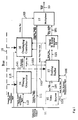
- FIG. 1 discloses the functional blocks of the display control apparatus in accordance with the invention.
- FIG. 2 discloses the functional blocks of the scaling buffer within the invention of FIG. 1.
- FIG. 3 discloses the functional blocks of the address controller within the invention of FIG. 1.
- FIG. 4 shows the procedures by which the initial value of the registers shown in address controller of FIG. 3 is set.
- FIG. 5 shows how the values of the registers shown in address controller of FIG. 3 are changed during the video scaling operation of the invention.
- FIG. 6 discloses the functional blocks of the timing generator within the invention of FIG. 1.
- FIG. 7 discloses the functional blocks of the overlay controller within the invention of FIG. 1.
- the display control apparatus of the invention receives the analog pixel data 111, vertical synchronization signal 115 and horizontal synchronization signal 113 from the computer graphics output 11 and outputs image data 13 switching between the analog pixel data 111 of the computer graphics and the video analog pixel data 181 of the video output.
- the control data are written into the registers within the apparatus via the controller bus 15 and the operation of the invention depends on the current values within the registers which will be more clear hereinafter.
- the controller may be any kind of the processor and the controller bus 15 includes data bus, address bus and read, write control signals to access the apparatus.
- the apparatus includes a timing generator 14, a scaling buffer 12, a overlay controller 16, a video source 10 and a digital to analog converter 18.
- the timing generator 14 is adapted to receive a horizontal synchronization signal 114 of the computer graphics output 11 and generates a pixel clock 143 of scaled video output and a horizontal lock signal 141.
- the scaling buffer 12 stores a video digital pixel data 101 therein and has an output port generating the scaled video output 121, responsive to the pixel clock 143 of scaled video output.
- the overlay controller 16 is coupled to the controller bus 15 and receives the analog pixel data 111 of the computer graphics output 11 and, responsive to the pixel clock 143 of scaled video output, the horizontal lock signal 141 and the vertical synchronization signal 115 of the computer graphics output 11, overlays the scaled video output 181 onto the computer graphics output 111 by generating the overlay key signal 163.
- the video source 10 outputs the video digital pixel data 101 in a well known manner.
- the video source 10 outputs the pixel data 101 to the scaling buffer 12 and the scaling buffer 12 stores the received data 101 into the two ports memory 20 therein shown in FIG. 2, based on the video pixel clock 103.
- the digital to analog converter 18 converts the scaled video digital pixel data 121 into the video analog pixel data 181, responsive to the pixel clock of the scaled video 143.
- the multiplexer 17 performs the switch operation on the input analog pixel data 111 of the computer graphics output and analog pixel data 181 of video output, in response to the overlay signal 163, and outputs the image data 13.
- the horizontal synchronization signal 105 from the video source 10 is the first timing point for each horizontal display of the video output 101 and also acts to access initial cell of the memory 20 within the scaling buffer 12. Accordingly, as the horizontal synchronization signal 105 is asserted, the video digital pixel data 101 are stored into the memory 20 starting from the first location of the cells.
- the window key signal 161 is asserted to reset the output address pointer 24 shown in FIG. 2 to assure the first digital pixel data 121 of the scaled video displayed within the video window comes from the first location of the memory.
- the controller may program the values of the registers of the scaling buffer 12, overlay controller 16 and timing generator 14 via controller bus 15.
- the values of the registers control the value of the video scaling factor, the target color regarding the generation of the target key signal, the area of the video window regarding the generation of the window key signal and the parameter of the horizontal pixel number of the scaled video regarding the timing generator 14.
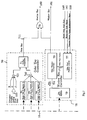
- the video scaling apparatus 12 comprises an address controller 26, an output address pointer 24, a two ports memory 20 and an input address pointer 22.
- the address controller 26 is adapted to receive a normal 311, a scale-down 312 and a scale-up 313 signal and generates an address increment signal 261 which has value corresponding to the scale factor value N/D designated.
- the output address pointer 24 generates an output address 241, responsive to the address increment signal 261 and the pixel clock 143 of the scaled video, to access the two ports memory 20.
- the dual ports memory 20 stores a video digital pixel data 101 therein and has an output port, responsive to the output address 241, generates the scaled video digital pixel data 121 corresponding to the scale factor value N/D.
- the dual ports memory 20 has an input port, responsive to the input address 221 provided by the input address pointer 22, receives the video digital pixel data 101. In order to place the input data on each adjacent memory location, a counter is used as the input address pointer 22.
- the video pixel clock 103 increments the value of the address pointer 22 such that the input data are stored in sequence.
- the video horizontal synchronization signal 105 forces the first pixel of each horizontal scan line to be stored at the first location of respective memory cells.
- an accumulator is used as the output address pointer 24 to fulfill the needs of the scaling operation.
- the value of the address increment signal 261 is accumulated into the output address pointer 24 to access another location of the memory 20.
- the address adjustment signal 263 is enabled to increment the output address pointer 24 by one. The detailed operation of the address adjustment signal 263 will be recited hereinafter.
- the address controller 26 comprises a control register 31 and address increment register 30, both coupled to the controller bus 15.
- the control register 31 generates the scale control signals, including the normal signal 311, the scale-down signal 312 and the scale-up signal 313.
- the address increment register 30 generates the address increment signal 261.
- the address controller 26 further comprises a criterion register 34 and a remain addend register 36 both of which are coupled to the controller bus 15.
- the remain addend register 36 has a first input receiving the scale-down signal 312 and a second input receiving the address adjustment signal 263.
- the address controller 26 further comprises a complement circuit 35 having a first input, coupled to an output of the criterion register 34, and a second input, adapted to receive the address adjustment signal 263, and a third input receiving the scale-up signal 313.
- the address controller 26 further comprises a remain accumulator 33 and a comparator 32.
- the remain accumulator 33 has a first input coupled to the output of the complement circuit 35 and a second input coupled to the output of the remain addend register 36.
- the remain accumulator 33 outputs its value, in response to the address adjustment signal 263, the pixel clock 143 of the scaled video.
- the comparator 32 compares the output of the criterion register 34 with the output of the remains accumulator 33 to generate the address adjustment signal 263.
- the comparator 32 has an input receiving the normal signal 311.
- the value stored in the address increment register 30 decides the basic increment value of the output address pointer 24.
- the criterion register 34 stores a reference value with which the remain accumulator 33 compares and by which at what condition the address adjustment signal 263 is to be enabled.
- the value of the remain addend register 36 is the basic accumulation value to the operation of the remain accumulator 33.
- the control register 31 generates the normal signal 311, the scale-down signal 312 or the scale-up signal 313 based on the value input from the controller bus 15 and stored therein.
- the values of all registers shown are programmed by the controller via controller bus 15.
- the window key signal 161 is used to reset the value of the remains accumulator 33 to zero.
- step 41 the controller reads the Denominator(D) and the Numerator(N) of the ratio form of the scaling factor.
- step 42 which compares the value of the D and N, as the value of scale factor indicates a scale down, the steps 43 and 44 are performed.
- step 43 divide the D by N and generates a quotient and remainder of D/N.
- step 44 the quotient of D/N is stored into the address increment register 30, the remainder of D/N is stored into the remain addend register 36 and the N is stored into the criterion register 34. Also in step 44, write the control register 31 to set the scale-down signal 312.
- step 46 is performed.
- step 46 a zero is stored into the address increment register 30, the N is stored into the remain addend register 36, the D is stored into the criterion register 34 and the control register 31 is written to set the scale-up signal 313.
- step 45 1 is stored into the address increment register 30 and the control register 31 is written to set the normal signal 311.
- the scaling buffer 12 takes over to execute the video image scaling.
- Each cycle of the pixel clock 143 of the scaled video updates the values of the output address pointer 24 and the remain accumulator 33 respectively based on the operation of the associated circuits connected thereto.
- the address adjustment signal 263 is thereby inactive. Accordingly, each time the scaling buffer 12 outputs one pixel data, the output address pointer 24 increments only by one indicating all pixel data are output without video enlargement or reduction effect.
- the output address pointer 24 increments by a value of the address increment signal 261, larger than one, output from address increment register 30 and, accordingly, some locations of the memory 20 are skipped during access indicating only the selected pixel data are output with a video reduction effect.
- step 53 test if the window key signal 161 is asserted. If it is not, in step 55, reset the remain accumulator 33 and afterwards go to step 53.
- step 57 check if the remain accumulator 33 is greater than the criterion register 34. If it is no in step 57, then in step 571, set the address adjustment signal 263 to be inactive, or logic 0, and the remains accumulator 33 also accumulates the value from the remain addend register 36, which indicates an truncation error of scaling factor, each time the pixel data is output. Afterwards, go to step 53. At times at which the value of error accumulated in the remain accumulator 33 exceeds the reference value in the criterion register 34 indicated by yes of the step 57, the invention performs the step 572. In step 572, set the address adjustment signal 263 active, or logic 1, and the remain accumulator 33 updates its value by adding its current value to the output of the remain addend register 36 minus the output of the criterion register 34.
- each time the scaling buffer 12 outputs one pixel data the output address pointer 24 increments by a zero output from address increment register 30 and, accordingly, each locations of the memory 20 are repeatedly accessed indicating the pixel data are output with a video enlargement effect.
- the number of access repetition process depends on the number of times required for the value in the criterion register 34 to reduce to a value smaller than the value in the remain accumulator 33.
- step 52 test if the window key signal 161 is asserted. If it is not, in step 54, reset the remain accumulator 33 and afterwards go to step 52.
- step 56 check if the remain accumulator 33 is greater than the remains accumulator 33. If it is yes in step 56 indicating same location of the memory 20 has to be accessed again, then in step 561, set the address adjustment signal 263 to be inactive, or logic 0, and reduce the remains accumulator 33 by the value of the criterion register 34. Afterwards, go to step 52. At times at which the value of remains accumulator 33 exceeds the reference value in the criterion register 34 indicating a next location of memory 20 is to be accessed, the invention performs the step 562. In step 562, set the address adjustment signal 263 active, or logic 1, and the remain accumulator 33 updates its value by adding its residual value of the last access operation to the output of the remain addend register 36 minus the output of the criterion register 34.
- the video scaling process is operated uniformly over the entire video.
- the timing generator 14 refers to the phase of the horizontal synchronization signal 113 of computer graphics output to produce the pixel clock 143 of scaled video and the horizontal lock signal 141 such that, while video being overlaid on the computer graphics, not only the required synchronization but also full screen display of video on any kinds of resolution of the computer graphics are achieved.
- the timing generator 14 is basically a phase lock loop which generates the pixel clock 143 of the scaled video in synchronization with the horizontal synchronization signal 113 of the computer graphics output.
- the timing generator 14 comprises a programmable frequency divider 61, a phase detector 63, a loop filter 65 and a voltage controlled oscillator 67.
- the programmable frequency divider 61 coupled to the controller bus 15, has an input receiving the pixel clock 143 of the scaled video and an output generating the horizontal lock signal 141.
- the controller via controller bus 15 programs the pixel number of the horizontal scan line of the video output into the programmable frequency divider 61. This pixel number is used by the frequency divider as its divisor to generate the horizontal lock signal 141 based on the frequency of the pixel clock 143 of the scaled video.
- the horizontal lock signal 141 is used as a horizontal synchronization signal for video output operation.
- the phase detector 63 generates a control signal 631 by comparing phase difference between the horizontal synchronization signal 113 and the horizontal lock signal 141.
- the loop filter 65 generates a filtered control signal 651 by filtering out a noise within the control signal 631.
- the voltage controlled oscillator 67 generates the pixel clock 143 of the scaled video, in response to the filtered control signal 651.
- the oscillation frequency of the pixel clock 143 varies according to the voltage of the control signal 651.
- the pixel clock 143 of the scaled video signal is also input to the frequency divider 61 to generate the horizontal lock signal 141.
- phase lock loop Since the operation of the phase lock loop, any phase difference between the horizontal lock signal 141 and horizontal synchronization signal 113 will diminish in the loop operation, and a final synchronization is achieved.
- the pixel clock 143 and the horizontal lock signal 141 are provided to the scaling buffer 12, digital to analog converter 18, programmable image overlay controller 16 as the pixel clock and the horizontal synchronization signal respectively.
- the image overlay controller 16 coupled to the controller bus 15 and receiving the analog pixel data 111 of the computer graphics output and, responsive to the pixel clock 143 of the video output, the horizontal lock signal 141, and the vertical synchronization signal 115 of the computer graphics output, generates the overlay key signal 163.
- the image overlay controller 16 comprises a first controller 70 and a second controller 78 and an AND gate 75.
- the first controller 70 generates a color key signal 711.
- the second controller 78 generates the window key signal 161.
- the AND gate 75 is adapted to receive the color key signal 711 and the window key signal 161, and generates the overlay key signal 163.
- the first controller 70 comprises an analog comparator 71 comparing the analog pixel data 111, which includes R, G, B components, of the computer graphics output with a target color, output from the corresponding Digital to Analog converter 721, 722 and 723, to generate the color key signal 711. Also included in the Digital to Analog converter 721, 722 and 723 are the corresponding register storing the target color input from the controller via the controller bus 15.
- the second controller 78 comprises a video window comparator 73 comparing the location of the video analog pixel data 771 with a predetermined video window 791 to generate the window key signal 161.
- the second controller 78 further comprises a position counter 77 receiving the pixel clock 143 of the scaled video, the horizontal lock signal 141 and the vertical synchronization signal 115 of the computer graphics, to generates the video pixel location 771.
- the controller programs the R, G, B component value of the registers within the D/A converter 721, 722, 723 to select the target color controlling the color key signal 711 and programs the video window register 79 to predetermine the area of the displayed video window via the controller bus 15.
- One analog comparator is required for comparison of each color component of the target color with the analog pixel data 111. Therefore, total of three analog comparators are required other than the complications of the associated circuits.
- the three components of target color within the D/A converters 721, 722, 723 and the three components of analog pixel data 111 of the computer graphics output are added first at the corresponding analog adder 741 and 742 respectively before comparison.
- the target color must be one having R, G, B components all being logic 1, or must be another one having R, G, B components all being logic 0. It is known it is black when R, G, B components all are logic 0 and it is white when R, G, B components all are logic 1.
- the color key signal 711 is enabled. Otherwise, the color key signal 711 is disabled.
- the controller transforms the upper-left corner coordinates, the height and the width of the video window into the locations of the video pixels corresponding to the four corners of the video window.
- the video window register 79 there are four registers used to save the four corner locations of the video window prescribed.
- the position counter 77 one horizontal counter is triggered by the horizontal lock signal 141 and another vertical counter is triggered by the vertical synchronization signal 115 of the computer graphics output.
- Counting the pixel clock 143 of the scaled video has the idea of the horizontal location of the present pixel data.
- Counting the horizontal lock signal 141 has the idea of the vertical location of the present pixel data.
- the output of these two counters form the video pixel position signal 771.
- the window key signal 161 is enabled. Otherwise, it is disabled.
- the enabled window key signal 161 not only affects the output of the AND gate 75 but also controls the operation of the scaling buffer 12.
- the AND gate 75 activates the overlay key signal 163 only when both the color key signal 711 and window key signal 161 are both active.
- the arrangement avoids the disadvantages of the implementation of the single color key approach or single window key approach.
Landscapes
- Engineering & Computer Science (AREA)
- Physics & Mathematics (AREA)
- General Physics & Mathematics (AREA)
- Theoretical Computer Science (AREA)
- Computer Hardware Design (AREA)
- Multimedia (AREA)
- Signal Processing (AREA)
- Controls And Circuits For Display Device (AREA)
- Studio Circuits (AREA)
Priority Applications (3)
| Application Number | Priority Date | Filing Date | Title |
|---|---|---|---|
| US08/434,974 US5710573A (en) | 1995-05-04 | 1995-05-04 | Scaled video output overlaid onto a computer graphics output |
| EP95106717A EP0741379A1 (fr) | 1995-05-04 | 1995-05-04 | Sortie vidéo à échelle variable superposée à une sortie graphique d'ordinateur |
| JP7124089A JP2896103B2 (ja) | 1995-05-04 | 1995-05-23 | コンピュータグラフィック出力にオーバーレイされたスケールされたビデオ出力発生装置 |
Applications Claiming Priority (3)
| Application Number | Priority Date | Filing Date | Title |
|---|---|---|---|
| US08/434,974 US5710573A (en) | 1995-05-04 | 1995-05-04 | Scaled video output overlaid onto a computer graphics output |
| EP95106717A EP0741379A1 (fr) | 1995-05-04 | 1995-05-04 | Sortie vidéo à échelle variable superposée à une sortie graphique d'ordinateur |
| JP7124089A JP2896103B2 (ja) | 1995-05-04 | 1995-05-23 | コンピュータグラフィック出力にオーバーレイされたスケールされたビデオ出力発生装置 |
Publications (1)
| Publication Number | Publication Date |
|---|---|
| EP0741379A1 true EP0741379A1 (fr) | 1996-11-06 |
Family
ID=27236524
Family Applications (1)
| Application Number | Title | Priority Date | Filing Date |
|---|---|---|---|
| EP95106717A Withdrawn EP0741379A1 (fr) | 1995-05-04 | 1995-05-04 | Sortie vidéo à échelle variable superposée à une sortie graphique d'ordinateur |
Country Status (3)
| Country | Link |
|---|---|
| US (1) | US5710573A (fr) |
| EP (1) | EP0741379A1 (fr) |
| JP (1) | JP2896103B2 (fr) |
Families Citing this family (28)
| Publication number | Priority date | Publication date | Assignee | Title |
|---|---|---|---|---|
| KR100211056B1 (ko) * | 1995-12-23 | 1999-07-15 | 이계철 | 다수개의 비디오에 대한 윈도우 제어방법 |
| US5917549A (en) * | 1996-08-07 | 1999-06-29 | Adobe Systems Incorporated | Transforming images with different pixel aspect ratios |
| US5838387A (en) * | 1996-12-20 | 1998-11-17 | Intel Corporation | Digital video scaling engine |
| US5796392A (en) | 1997-02-24 | 1998-08-18 | Paradise Electronics, Inc. | Method and apparatus for clock recovery in a digital display unit |
| US6486922B1 (en) * | 1998-02-20 | 2002-11-26 | Matsushita Electric Industrial Co., Ltd. | Synchronization method of image decoder |
| US6396536B1 (en) | 1998-05-27 | 2002-05-28 | Advanced Testing Technologies, Inc. | Automatic test instrument for multi-format video generation and capture |
| US7768533B2 (en) | 1998-05-27 | 2010-08-03 | Advanced Testing Technologies, Inc. | Video generator with NTSC/PAL conversion capability |
| US7253792B2 (en) * | 1998-05-27 | 2007-08-07 | Advanced Testing Technologies, Inc. | Video generation and capture techniques |
| US7495674B2 (en) * | 1998-05-27 | 2009-02-24 | Advanced Testing Technologies, Inc. | Video generation and capture techniques |
| USRE45960E1 (en) | 1998-05-27 | 2016-03-29 | Advanced Testing Technologies, Inc. | Single instrument/card for video applications |
| US7978218B2 (en) * | 1998-05-27 | 2011-07-12 | Advanced Testing Technologies Inc. | Single instrument/card for video applications |
| US20020033780A1 (en) * | 1998-09-30 | 2002-03-21 | Masanobu Kimoto | Auto sizing and positioning video data using generalized timing formula |
| US6621499B1 (en) * | 1999-01-04 | 2003-09-16 | Ati International Srl | Video processor with multiple overlay generators and/or flexible bidirectional video data port |
| JP3797838B2 (ja) * | 1999-12-15 | 2006-07-19 | 三菱電機株式会社 | 画像表示装置 |
| US6724948B1 (en) * | 1999-12-27 | 2004-04-20 | Intel Corporation | Scaling images for display |
| DE10159469B4 (de) * | 2000-12-29 | 2011-09-29 | Robert Bosch Gmbh | Verfahren zur Anzeige und Anzeigevorrichtung |
| US6806888B2 (en) | 2002-01-15 | 2004-10-19 | International Business Machines Corporation | Method, apparatus, and computer program product for generating, from first information for a first image, second information for a second image corresponding to a portion of the first image |
| US8166388B2 (en) * | 2002-05-14 | 2012-04-24 | Microsoft Corporation | Overlaying electronic ink |
| US7925987B2 (en) * | 2002-05-14 | 2011-04-12 | Microsoft Corporation | Entry and editing of electronic ink |
| US7158675B2 (en) | 2002-05-14 | 2007-01-02 | Microsoft Corporation | Interfacing with ink |
| US20030214553A1 (en) * | 2002-05-14 | 2003-11-20 | Microsoft Corporation | Ink regions in an overlay control |
| US20030214531A1 (en) * | 2002-05-14 | 2003-11-20 | Microsoft Corporation | Ink input mechanisms |
| US7171622B2 (en) | 2002-07-18 | 2007-01-30 | International Business Machines Corporation | Method, apparatus and computer program product for projecting objects in a display unit |
| KR100580177B1 (ko) * | 2003-09-22 | 2006-05-15 | 삼성전자주식회사 | 디지털 방송 수신 시스템에서 디스플레이 동기 신호 생성 장치 및 디코더와 그 방법 |
| US20050068336A1 (en) * | 2003-09-26 | 2005-03-31 | Phil Van Dyke | Image overlay apparatus and method for operating the same |
| US7250983B2 (en) * | 2004-08-04 | 2007-07-31 | Trident Technologies, Inc. | System and method for overlaying images from multiple video sources on a display device |
| US8497908B1 (en) | 2011-12-13 | 2013-07-30 | Advanced Testing Technologies, Inc. | Unified video test apparatus |
| US8648869B1 (en) | 2012-02-13 | 2014-02-11 | Advanced Testing Technologies, Inc. | Automatic test instrument for video generation and capture combined with real-time image redisplay methods |
Citations (8)
| Publication number | Priority date | Publication date | Assignee | Title |
|---|---|---|---|---|
| US4825388A (en) * | 1986-04-01 | 1989-04-25 | Princeton Gamma Tech., Inc. | Apparatus and method for processing digital images |
| EP0384257A2 (fr) * | 1989-02-23 | 1990-08-29 | International Business Machines Corporation | Affichage audio vidéo interactif |
| US5068731A (en) * | 1988-07-14 | 1991-11-26 | Seiko Epson Corporation | Video image enlargement and reduction system and method |
| GB2245394A (en) * | 1990-06-18 | 1992-01-02 | Rank Cintel Ltd | Video framestore selective addressing system |
| EP0484981A2 (fr) * | 1990-11-09 | 1992-05-13 | Fuji Photo Film Co., Ltd. | Dispositif de traitement de données d'image |
| US5150461A (en) * | 1988-05-25 | 1992-09-22 | Sun Electric Corporation | Fixed point method of video display scaling |
| EP0610829A1 (fr) * | 1993-02-05 | 1994-08-17 | Brooktree Corporation | Système et procédé pour l'affichage sur un écran de visualisation, d'information provenant d'une mémoire graphique et d'une mémoire vidéo |
| US5398075A (en) * | 1993-11-19 | 1995-03-14 | Intel Corporation | Analog chroma keying on color data |
Family Cites Families (12)
| Publication number | Priority date | Publication date | Assignee | Title |
|---|---|---|---|---|
| JPH0685556B2 (ja) * | 1984-03-30 | 1994-10-26 | 大日本スクリ−ン製造株式会社 | 画像走査記録装置における倍率変換方法 |
| US4580165A (en) * | 1984-04-12 | 1986-04-01 | General Electric Company | Graphic video overlay system providing stable computer graphics overlayed with video image |
| US4821031A (en) * | 1988-01-20 | 1989-04-11 | International Computers Limited | Image display apparatus |
| US5387945A (en) * | 1988-07-13 | 1995-02-07 | Seiko Epson Corporation | Video multiplexing system for superimposition of scalable video streams upon a background video data stream |
| JPH02259797A (ja) * | 1989-03-31 | 1990-10-22 | Toshiba Corp | 画像メモリ装置 |
| JPH0418681A (ja) * | 1990-05-11 | 1992-01-22 | Nec Corp | 画像縮小・拡大パターン生成回路 |
| JPH04241389A (ja) * | 1991-01-14 | 1992-08-28 | Sharp Corp | 画像処理装置 |
| US5422678A (en) * | 1991-01-29 | 1995-06-06 | Seiko Epson Corp. | Video processor for enlarging and contracting an image in a vertical direction |
| JPH04317099A (ja) * | 1991-04-16 | 1992-11-09 | Matsushita Electric Ind Co Ltd | 動画対応フレームバッファ |
| JPH05158464A (ja) * | 1991-12-09 | 1993-06-25 | Toshiba Corp | 解像度変換回路 |
| JPH05242232A (ja) * | 1992-02-28 | 1993-09-21 | Hitachi Ltd | 情報処理装置及び映像表示装置 |
| US5541666A (en) * | 1994-07-06 | 1996-07-30 | General Instrument | Method and apparatus for overlaying digitally generated graphics over an analog video signal |
-
1995
- 1995-05-04 EP EP95106717A patent/EP0741379A1/fr not_active Withdrawn
- 1995-05-04 US US08/434,974 patent/US5710573A/en not_active Expired - Lifetime
- 1995-05-23 JP JP7124089A patent/JP2896103B2/ja not_active Expired - Lifetime
Patent Citations (8)
| Publication number | Priority date | Publication date | Assignee | Title |
|---|---|---|---|---|
| US4825388A (en) * | 1986-04-01 | 1989-04-25 | Princeton Gamma Tech., Inc. | Apparatus and method for processing digital images |
| US5150461A (en) * | 1988-05-25 | 1992-09-22 | Sun Electric Corporation | Fixed point method of video display scaling |
| US5068731A (en) * | 1988-07-14 | 1991-11-26 | Seiko Epson Corporation | Video image enlargement and reduction system and method |
| EP0384257A2 (fr) * | 1989-02-23 | 1990-08-29 | International Business Machines Corporation | Affichage audio vidéo interactif |
| GB2245394A (en) * | 1990-06-18 | 1992-01-02 | Rank Cintel Ltd | Video framestore selective addressing system |
| EP0484981A2 (fr) * | 1990-11-09 | 1992-05-13 | Fuji Photo Film Co., Ltd. | Dispositif de traitement de données d'image |
| EP0610829A1 (fr) * | 1993-02-05 | 1994-08-17 | Brooktree Corporation | Système et procédé pour l'affichage sur un écran de visualisation, d'information provenant d'une mémoire graphique et d'une mémoire vidéo |
| US5398075A (en) * | 1993-11-19 | 1995-03-14 | Intel Corporation | Analog chroma keying on color data |
Non-Patent Citations (1)
| Title |
|---|
| U. TIETZE, CH. SCHENK: "Halbleiter-Schaltungstechnik", 1993, SPRINGER-VERLAG, BERLIN, HEIDELBERG, NEW YORK * |
Also Published As
| Publication number | Publication date |
|---|---|
| JP2896103B2 (ja) | 1999-05-31 |
| JPH08314420A (ja) | 1996-11-29 |
| US5710573A (en) | 1998-01-20 |
Similar Documents
| Publication | Publication Date | Title |
|---|---|---|
| US5710573A (en) | Scaled video output overlaid onto a computer graphics output | |
| KR100303723B1 (ko) | 이미지업스케일방법및장치 | |
| EP1164568B1 (fr) | Dispositif et procede de conversion de signaux video | |
| JPH1079905A (ja) | ディジタルディスプレイ装置の画像サイズ調整方法及びその画像サイズ調整回路 | |
| KR100359816B1 (ko) | 포맷 변환 장치 | |
| KR20010007528A (ko) | 동기 변환 장치 및 방법 및 매체 | |
| KR20000011488A (ko) | 디지털영상데이터의저장및복구를위한방법및장치 | |
| US20060262223A1 (en) | Video scalers having reduced output memory and methods for selecting output memory size | |
| KR0164670B1 (ko) | 컴퓨터 그래픽 출력에 축척된 영상출력을 중첩하는 디스플레이 제어장치 | |
| KR100237422B1 (ko) | Lcd 모니터 표시장치 및 그 표시방법 | |
| US20060170954A1 (en) | Method and system for generating synchronous multidimensional data streams from a one -dimensional data stream | |
| JP3022664B2 (ja) | 画像表示サイズ可変回路 | |
| US8345161B2 (en) | Signal processing device, and image output device | |
| KR100197606B1 (ko) | 확대기능을 구비한 스틸카메라 | |
| JPH1115428A (ja) | 水平表示幅調整回路 | |
| JPH03102982A (ja) | 特殊効果装置 | |
| US6873370B1 (en) | Method and circuit arrangement for picture-in-picture fade-in | |
| JP4003508B2 (ja) | 画像合成装置及び画像合成方法 | |
| JP3646839B2 (ja) | デジタルオシロスコープ | |
| JPH1063219A (ja) | 表示装置及びその駆動方法 | |
| JP3518215B2 (ja) | 映像表示装置 | |
| JPH09182042A (ja) | クロック位相同期回路 | |
| JPS6343949B2 (fr) | ||
| KR100347168B1 (ko) | 와이드스크린텔레비전용비디오압축회로 | |
| KR20030060617A (ko) | 가변 구조 포맷변환 장치 및 방법 |
Legal Events
| Date | Code | Title | Description |
|---|---|---|---|
| PUAI | Public reference made under article 153(3) epc to a published international application that has entered the european phase |
Free format text: ORIGINAL CODE: 0009012 |
|
| 17P | Request for examination filed |
Effective date: 19950504 |
|
| AK | Designated contracting states |
Kind code of ref document: A1 Designated state(s): BE DE FR GB IT NL |
|
| 17Q | First examination report despatched |
Effective date: 20020212 |
|
| STAA | Information on the status of an ep patent application or granted ep patent |
Free format text: STATUS: THE APPLICATION IS DEEMED TO BE WITHDRAWN |
|
| 18D | Application deemed to be withdrawn |
Effective date: 20020823 |