EP0743685A2 - Nichtflüchtiger Halbleiterspeicher, der die Polarization eines ferroelektrischen Materials braucht - Google Patents
Nichtflüchtiger Halbleiterspeicher, der die Polarization eines ferroelektrischen Materials braucht Download PDFInfo
- Publication number
- EP0743685A2 EP0743685A2 EP96108018A EP96108018A EP0743685A2 EP 0743685 A2 EP0743685 A2 EP 0743685A2 EP 96108018 A EP96108018 A EP 96108018A EP 96108018 A EP96108018 A EP 96108018A EP 0743685 A2 EP0743685 A2 EP 0743685A2
- Authority
- EP
- European Patent Office
- Prior art keywords
- film
- semiconductor memory
- nonvolatile semiconductor
- gate electrode
- ferroelectric material
- Prior art date
- Legal status (The legal status is an assumption and is not a legal conclusion. Google has not performed a legal analysis and makes no representation as to the accuracy of the status listed.)
- Granted
Links
Images


Classifications
-
- H—ELECTRICITY
- H10—SEMICONDUCTOR DEVICES; ELECTRIC SOLID-STATE DEVICES NOT OTHERWISE PROVIDED FOR
- H10D—INORGANIC ELECTRIC SEMICONDUCTOR DEVICES
- H10D30/00—Field-effect transistors [FET]
- H10D30/60—Insulated-gate field-effect transistors [IGFET]
- H10D30/701—IGFETs having ferroelectric gate insulators, e.g. ferroelectric FETs
Definitions
- the present invention relates to a nonvolatile semiconductor memory, and more specifically to a nonvolatile semiconductor memory configured to store information by utilizing polarization of a ferroelectric material.
- a nonvolatile semiconductor memory utilizing a ferroelectric material as a medium for storing information has an advantage that if deterioration of a ferroelectric material film does not occur, information can be stored for a long term of time, and further, is expected that it can make it possible to reduce a memory cell size and therefore to realize a memory having a large storage capacity.
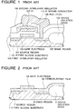
- a device isolation oxide film (field oxide) 102 is formed by a selective oxidation such as a LOCOS (local oxidation of silicon) process, and within an active region confined by the device isolation oxide film, a gate electrode 103 is formed through a gate insulator film on the surface of the substrate.
- a source region 104 and a drain region 105 are formed in a surface region of the substrate at opposite sides of the gate electrode 103, so as to locate the gate electrode between the source region and the drain region.
- a first interlayer insulator film 106 is formed to cover a whole surface of the substrate, and a Pt film 107 is formed on the first interlayer insulator film 106, above a position of the gate electrode 103. Furthermore, a PZT (PbZr 1-x Ti x O 3 ) film 108 is formed to cover the Pt film 107. A second interlayer insulator film 109 is formed to cover a whole surface of the substrate including the PZT film 108. In addition, contact holes are formed to reach the drain region 105 and the PZT film 108, respectively, and an aluminum wiring conductor 110 is formed on the second interlayer insulator film 109 to contact with the drain region 105 and the PZT film 108 through the contact holes.
- PZT PbZr 1-x Ti x O 3
- FIG. 2 there is shown a diagrammatic section view illustrating another example of a conventional nonvolatile semiconductor memory utilizing a ferroelectric material film, in which a gate insulator film of a transistor is formed of a ferroelectric material film.
- a device isolation oxide film 2 is formed on a principal surface of a P-type silicon substrate 1, and a ferroelectric material film 4C is formed on the principal surface of the substrate 1 to constitute a gate insulator film.
- a gate electrode 5A is formed on the ferroelectric material film 4C, and a source region 7 and a drain region 8 are formed in a surface region of the substrate at opposite sides of the gate electrode 5A, so as to locate the gate electrode between the source region and the drain region.
- the ferroelectric material of the gate insulator film which is now under consideration, is BaMgF 4 and PbZr 1-x Ti x O 3 .
- each memory cell consists of a transistor part and a memory part, the structure is complicated. This is inconvenient to microminiaturization.
- a coercive electric field (applied electric field when polarization reversal starts) of the PbZr 1-x Ti x O 3 film is on the order of 80 kV/cm, and a dielectric constant of the PbZr 1-x Ti x O 3 film is on the order of 1000.
- the natural oxide film is not an intentionally formed film, the natural oxide film is not so good in film quality, so that there is high possibility that if a high electric field as mentioned above is applied, the natural oxide film is broken down.
- the PbZr 1-x Ti x O 3 film is formed to have a thickness of 100 nm, it is necessary to apply a voltage of 0.8 V across the PbZr 1-x Ti x O 3 film in order to apply a necessary coercive electric field.
- the gate insulator film is formed of BaMgF 4 , no natural oxide film is formed since BaMgF 4 does not include an oxidizing specie.
- polarizability of this material is relatively low.
- the BaMgF 4 film contains a crystal defect, the polarizability further lowers. Therefore, in order to constitute a satisfactory memory, it is necessary to form a BaMgF 4 film having an excellent film quality, namely, less crystal defect. However, this is not so easy because of difference in lattice constant between BaMgF 4 and a silicon substrate and because of other causes.
- ferroelectric materials other than oxides having a low dielectric constant Since there exist ferroelectric materials other than oxides having a low dielectric constant, it is possible to prevent formation of the natural oxide by using the ferroelectric materials other than oxides. However, these ferroelectric materials are small in polarizability and poor in heat resistive property, and therefore, it is difficult to use these ferroelectric materials as a material used for manufacturing a semiconductor device.
- Another object of the present invention is to provide a nonvolatile semiconductor memory configured to store information by utilizing polarization of a ferroelectric material, the nonvolatile semiconductor memory having a simple construction and a high reliability and being easy to manufacture and to microminiaturize, the nonvolatile semiconductor memory being able to be driven with a low voltage.
- a nonvolatile semiconductor memory comprising a semiconductor substrate, a gate electrode formed through a gate insulator film on a principal surface of the semiconductor substrate, a pair of source/drain regions formed in a principal surface region of the semiconductor substrate to locate the gate electrode between the pair of source/drain regions, the gate insulator film being formed of a first insulating film in contact with the principal surface of the semiconductor substrate, and a second insulating film formed on the first insulating film, the second insulating film being formed of a ferroelectric oxide having a dielectric constant of not larger than 50.
- the second insulating film includes a material selected from a group consisting of Pb 5 Ge 3 O 11 , LiTaO 3 , YMnO 3 , YbMnO 3 , ErMnO 3 and HoMnO 3 .
- the first insulating film is formed of a film selected from the group consisting of a silicon oxide film, a silicon oxynitride film and a laminated layer composed of an underlying silicon oxide film and an overlying silicon nitride film.
- a silicon oxide film or a silicon nitride film is preferably formed between the second insulating film and the gate electrode.
- the ferroelectric material film provided as the gate insulator film is required to have a film thickness on the order of 50 nm to 200 nm. Assuming that the ferroelectric material film has the coercive electric field of 80 kV/cm, it is necessary to apply a voltage of 0.4 V to 1.6 V across the ferroelectric material film. Under this condition, on the other hand, a voltage of 0.2 V is applied across the natural oxide film. Accordingly, it is possible to start polarization by applying a voltage of 0.6 V to 1.8 V to the gate electrode. Thus, even considering that it is necessary to apply a voltage higher than that voltage by several ten percents in order to cause a complete polarization, it is possible to drive the memory with an extremely low voltage.
- oxide ferroelectric materials are not deteriorated even if a semiconductor device manufacturing temperature is applied.
- FIG. 3A to 3D there are shown diagrammatic sectional views illustrating a process for manufacturing a first embodiment of the nonvolatile semiconductor memory in accordance with the present invention utilizing polarization of a ferroelectric material.
- a device isolation oxide film (field oxide) 2 is formed by a selective oxidation such as a LOCOS (local oxidation of silicon) process.
- a thermal oxidation is carried out in a low pressure atmosphere (for example, 1 Torr) at a temperature of 800°C, so as to form a thin oxide film having a thickness of 1.5 nm on the principal surface of the substrate 1.
- the thermal oxide film is lamp-heated within a NH 3 atmosphere so that an oxynitride film 3 is formed on the surface of the substrate.
- an ethylate (or ethoxide) of lead and an ethylate of germanium are prepared, and then, mixed to have a composition ratio of 5 : 3.
- the obtained mixture is deposited on the oxynitride film 3 by a sol gel process.
- an annealing is carried out within a dry oxygen atmosphere at 650°C for one hour. With this treatment, a film 4 of Pb 5 Ge 3 O 11 (lead germanate film) having a thickness of 100 nm is formed on the oxynitride film 3 as shown in Figure 3A.
- a dry etching using a chlorine containing gas is performed to pattern the TiN film 5 so as to form a gate electrode.
- a chlorine containing gas is performed to pattern the TiN film 5 so as to form a gate electrode.
- arsenic (As) is ion-implanted to form a source region 7 and a drain region 8 in a surface region of the substrate 1, as shown in Figure 3C.
- the photoresist film 6 is ashed in an oxygen plasma so that the photoresist film 6 is removed as shown in Figure 3D.
- the gate electrode (TiN film 5) is formed on the Pb 5 Ge 3 O 11 film 4 at the room temperature.
- a heat treatment is performed after formation of an upper electrode, and in the case that the gate electrode itself is formed at a high temperature process, it is preferred to form a silicon oxide film or a silicon nitride film, at a boundary between the Pb 5 Ge 3 O 11 film 4 and the gate electrode, namely, on the Pb 5 Ge 3 O 11 film 4 before deposition of the gate electrode layer, in order to prevent reaction between the Pb 5 Ge 3 O 11 film 4 and the gate electrode metal.
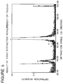
- a lead germanate film was formed on a whole surface of a silicon substrate by a sol gel process. Scanning electron microscope photographs of a surface and a section of the lead germanate film thus formed are shown in Figures 4A and 4B. From these photographs, it would be seen that a film having a smooth surface and a thickness on the order of 900 ⁇ is formed on the silicon substrate. Furthermore, the result of an X-ray diffraction measurement of the lead germanate film thus formed is shown in Figure 5. It would also be seen that the lead germanate film thus formed is polycrystalline.
- a TiN film (used for constituting the gate electrode) was formed on the lead germanate film thus formed, and a dielectric constant and a hysteresis characteristics were measured.
- the result of the measurement is that the dielectric constant is about 18.3 and the residual dielectric polarization is about 1.2 ⁇ C/cm 2 .
- a lead germanate film having a thickness of 3000 ⁇ was formed on a Pt electrode by the above mentioned sol gel process.
- This lead germanate film having the thickness of 3000 ⁇ had the coercive electric field of 14 kV/cm and the residual dielectric polarization of about 1.6 ⁇ C/cm 2 . Therefore, it would be understood that polarization reversal occurs by applying a voltage on the order of 0.4 V to the lead germanate film.
- the oxynitride film having the thickness of 2 nm converted into an oxide film thickness under the ferroelectric material film, there is formed the oxynitride film having the thickness of 2 nm converted into an oxide film thickness. Therefore, in the case of polarizing the lead germanate film having the thickness of 100 nm used in the actual device, a voltage applied across the natural oxide film is on the order of 0.013 V. This means that the natural oxide film is applied with only a voltage of 1/300 of the voltage applied in the case of the PZT film. This is considered to be attributable to the fact that both the dielectric constant and the coercive electric field of the ferroelectric material became small.
- an electric charge required to actually operate the device as a memory is on the order of 0.5 ⁇ C/cm 2 . Therefore, the residual dielectric polarization of about 1.6 ⁇ C/cm 2 , which could have been confirmed at present, is a satisfactory value.
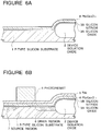
- FIG. 6A to 6D there are shown diagrammatic sectional views illustrating a process for manufacturing a second embodiment of the nonvolatile semiconductor memory in accordance with the present invention utilizing polarization of a ferroelectric material.
- a device isolation oxide film 2 is formed by a selective oxidation process. Then, the substrate 1 is heated to a temperature of 800°C, and then, is exposed to an oxygen gas diluted by a nitrogen gas, so that a silicon oxide film 3A having a thickness of 1.5 nm is formed on the surface of the substrate 1. Furthermore, a silicon nitride film 3B having a thickness of about 2 nm is formed on the silicon oxide film 3A by a low pressure CVD process.
- an oxide of Pb and Ge is deposited to form a film having a thickness of about 200 nm.
- the molar ratio of Pb and Ge in the target is 2.5 : 1. Namely, Pb is richer than Ge.
- the sputtering condition is that the substrate temperature is 450°C, and the plasma is generated in an atmosphere consisting of 90% of Ar and 10% of oxygen under a pressure of 6 mTorr.
- the reason for why the proportion of Pb drops as compared with the molar ratio in the target, is considered to be that lead evaporated at the temperature of 450°C.
- a TiN film 5 having a thickness of 100 nm is deposited on the Pb 5 Ge 3 O 11 film 4 by a sputtering.
- a photoresist film is deposited, and exposure and development are carried out to form a patterned photoresist film 6 having a pattern for the gate electrode.
- arsenic (As) is ion-implanted to form a source region 7 and a drain region 8 in a surface region of the substrate 1, as shown in Figure 6B.
- a dry etching is performed to remove the TiN film 5 and the Pb 5 Ge 3 O 11 film 4 which are not covered with the patterned photoresist film 6, so that a gate electrode is formed as shown in Figure 6C.
- a silicon oxide film having a thickness of 200 nm is deposited by a CVD process with a substrate temperature of 400°C, so as to form an interlayer insulator film 9 which completely covers the whole surface.
- a contact hole is formed to reach the drain region 8, and an aluminum alloy film is deposited and patterned to form a wiring conductor 10 contacting to the drain region 8 through the contact hole, as shown in Figure 6D.
- This wiring conductor 10 constitutes a bit line.
- the source region 7 is connected in common to a source region of other memory cells by means of a diffused layer (not shown) formed in the substrate.
- peripheral circuit can be formed in the same process as that for manufacturing a peripheral circuit in a conventional memory. In the present invention, however, it is preferred to previously form the peripheral circuit, prior to formation of the memory cells. But, if the peripheral circuit can be formed in a process of not higher than 700°C, the peripheral circuit can be formed after the formation of the memory cells.
- the source region is connected in common to the source region of other memory cells by means of the diffused layer formed in the substrate, but can be connected through a wiring conductor.
- the transistor is on-off controlled by direction of the polarization of the Pb 5 Ge 3 O 11 film 4. Therefore, the memory as mentioned above can be operated as a nonvolatile memory.
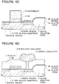
- FIGS. 7A to 7D there are shown diagrammatic sectional views illustrating a process for manufacturing a third embodiment of the nonvolatile semiconductor memory in accordance with the present invention utilizing polarization of a ferroelectric material.
- a device isolation oxide film 2 is formed by a selective oxidation process. Then, the substrate 1 is heated to a temperature of 800°C, and then, is exposed to an oxygen gas diluted by a nitrogen gas, so that a silicon oxide film 3A having a thickness of 1.5 nm is formed on the surface of the substrate 1. Furthermore, a silicon nitride film 3B having a thickness of about 3 nm is formed on the silicon oxide film 3A by a low pressure CVD process.
- an oxide of Li and Ta is deposited to form a film having a thickness of about 200 nm.
- the sputtering condition is that the substrate temperature is 560°C, and the plasma is generated in an atmosphere consisting of 90% of Ar and 10% of oxygen under a pressure of 6 mTorr.
- a molar ratio of Li : Ta is about 1 : 1.
- an oxidizing treatment is performed on this film within an oxygen atmosphere at a temperature of 1100°C for thirty seconds. From the X-ray diffraction analysis of this film, it was confirmed that the film thus formed is a LiTaO 3 film 4A ( Figure 7A).
- a TiN film 5 having a thickness of 100 nm is deposited on the LiTaO 3 film 4A thus formed, by sputtering at a room temperature.
- a photoresist film is deposited, and exposure and development are carried out to form a patterned photoresist film 6 having a pattern for the gate electrode.
- arsenic (As) is ion-implanted to form a source region 7 and a drain region 8 in a surface region of the substrate 1, as shown in Figure 7B.
- a dry etching is performed to remove the TiN film 5 and the LiTaO 3 film 4A which are not covered with the patterned photoresist film 6, so that a gate electrode is formed as shown in Figure 7C.
- a silicon oxide film having a thickness of 200 nm is deposited by a CVD process with a substrate temperature of 400°C, so as to form an interlayer insulator film 9 which completely covers the whole surface.
- a contact hole is formed to reach the drain region 8, and an aluminum alloy film is deposited and patterned to form a wiring conductor 10 contacting to the drain region 8 through the contact hole, as shown in Figure 7D.
- This wiring conductor 10 constitutes a bit line.
- the source region 7 is connected in common to source regions of other memory cells by means of a diffused layer (not shown) formed in the substrate, similarly to the other embodiments.
- the method for manufacturing the third embodiment of the memory cell in the nonvolatile semiconductor memory has been described.
- the reason for this is that since Li is easy to diffuse, contamination of the device must be made as small as possible.
- the silicon nitride film formed under the LiTaO 3 film is a film required as a barrier for preventing diffusion of Li.
- the silicon oxide film is provided as a lowermost layer, for the purpose of reducing energy levels at a boundary so as to elevate performance of the transistor.
- the dielectric constant of the LiTaO 3 film 4A thus formed was about 45. It was confirmed that the transistor can be on-off controlled by direction of the polarization of the LiTaO 3 film 4A, and therefore, this memory as mentioned above can be operated as a nonvolatile memory.
- the fourth embodiment is characterized in that a YMnO 3 film 4B is formed in place of the LiTaO 3 film 4A in the third embodiment. Since the process other than a step of forming the YMnO 3 film 4B is the same as a corresponding process of the third embodiment, only the step of forming the YMnO 3 film 4B will be described in the following.
- an oxide of Y and Mn is deposited on the silicon nitride film 3B to form a film having a thickness of about 150 nm.
- the sputtering condition is that the substrate temperature is 600°C, and the plasma is generated in an atmosphere consisting of 90% of Ar and 10% of oxygen under a pressure of 10 mTorr.
- a molar ratio of Y : Mn is about 1 : 1.
- an oxidizing treatment is performed on this film within an oxygen atmosphere at a temperature of 800°C for sixty seconds. From the X-ray diffraction analysis of this film, it was confirmed that the film thus formed is a YMnO 3 film ( Figure 7A).
- the nonvolatile semiconductor memory in accordance with the present invention is characterized in that a gate insulator film of a MOS transistor is formed of a ferroelectric material having a dielectric constant of not larger than 50.
- a gate insulator film of a MOS transistor is formed of a ferroelectric material having a dielectric constant of not larger than 50.
Landscapes
- Semiconductor Memories (AREA)
- Non-Volatile Memory (AREA)
Applications Claiming Priority (3)
| Application Number | Priority Date | Filing Date | Title |
|---|---|---|---|
| JP14236595 | 1995-05-18 | ||
| JP142365/95 | 1995-05-18 | ||
| JP7142365A JP2907322B2 (ja) | 1995-05-18 | 1995-05-18 | 不揮発性半導体記憶装置 |
Publications (3)
| Publication Number | Publication Date |
|---|---|
| EP0743685A2 true EP0743685A2 (de) | 1996-11-20 |
| EP0743685A3 EP0743685A3 (de) | 1997-01-29 |
| EP0743685B1 EP0743685B1 (de) | 2002-09-25 |
Family
ID=15313696
Family Applications (1)
| Application Number | Title | Priority Date | Filing Date |
|---|---|---|---|
| EP96108018A Expired - Lifetime EP0743685B1 (de) | 1995-05-18 | 1996-05-20 | Nichtflüchtiger Halbleiterspeicher, der die Polarization eines ferroelektrischen Materials braucht |
Country Status (5)
| Country | Link |
|---|---|
| US (1) | US6515322B1 (de) |
| EP (1) | EP0743685B1 (de) |
| JP (1) | JP2907322B2 (de) |
| KR (1) | KR100247884B1 (de) |
| DE (1) | DE69623850T2 (de) |
Cited By (2)
| Publication number | Priority date | Publication date | Assignee | Title |
|---|---|---|---|---|
| EP0936675A3 (de) * | 1998-01-02 | 2001-08-08 | Sharp Kabushiki Kaisha | C-Achse orientierte ferroelektrische Dünnschichttransistorzelle und deren Herstellungsverfahren |
| US6586260B2 (en) * | 2001-03-28 | 2003-07-01 | Sharp Laboratories Of America, Inc. | Single c-axis PGO thin film electrodes having good surface smoothness and uniformity and methods for making the same |
Families Citing this family (5)
| Publication number | Priority date | Publication date | Assignee | Title |
|---|---|---|---|---|
| JP3137880B2 (ja) * | 1995-08-25 | 2001-02-26 | ティーディーケイ株式会社 | 強誘電体薄膜、電子デバイスおよび強誘電体薄膜の製造方法 |
| KR100363393B1 (ko) * | 2000-06-28 | 2002-11-30 | 한국과학기술연구원 | 비파괴판독형 불휘발성 기억소자의 메모리 셀 소자 및 그제조 방법 |
| US20050082624A1 (en) * | 2003-10-20 | 2005-04-21 | Evgeni Gousev | Germanate gate dielectrics for semiconductor devices |
| KR102050034B1 (ko) * | 2018-03-22 | 2019-11-28 | 서울대학교산학협력단 | 비휘발성 메모리 소자용 재료 및 이의 제조방법 |
| KR20230041633A (ko) | 2021-09-17 | 2023-03-24 | 삼성전자주식회사 | 반도체 소자 및 이를 포함하는 전자 장치 |
Family Cites Families (20)
| Publication number | Priority date | Publication date | Assignee | Title |
|---|---|---|---|---|
| US3591852A (en) * | 1969-01-21 | 1971-07-06 | Gen Electric | Nonvolatile field effect transistor counter |
| GB8424668D0 (en) * | 1984-09-29 | 1984-11-07 | Plessey Co Plc | Optical waveguides |
| JPS6338248A (ja) * | 1986-08-04 | 1988-02-18 | Hitachi Ltd | 半導体装置およびその製造方法 |
| JPH0517139A (ja) * | 1991-07-12 | 1993-01-26 | Ube Ind Ltd | アモルフアス強誘電体酸化物材料及びその製造方法 |
| JPH0517137A (ja) * | 1991-07-12 | 1993-01-26 | Ube Ind Ltd | アモルフアス強誘電体酸化物材料及びその製造方法 |
| JP2932777B2 (ja) | 1991-07-31 | 1999-08-09 | スズキ株式会社 | V型エンジンの補機取付構造 |
| EP0540993A1 (de) | 1991-11-06 | 1993-05-12 | Ramtron International Corporation | Struktur und Herstellung eines MOS-Feldeffekttransistors mit hoher Transkonduktanz unter Verwendung eines Gatedielektrikums, das aus einer übereinanderliegenden Pufferschicht/Ferroelektrikum/Pufferschicht besteht |
| JPH05139730A (ja) * | 1991-11-15 | 1993-06-08 | Ube Ind Ltd | アモルフアス強誘電体酸化物材料及びその製造方法 |
| EP0784347A2 (de) * | 1992-06-18 | 1997-07-16 | Matsushita Electronics Corporation | Halbleiterbauelement mit Kondensator |
| JPH06151762A (ja) * | 1992-11-13 | 1994-05-31 | Ricoh Co Ltd | 強誘電体材料およびそれを使用した強誘電体メモリ素子 |
| US5666305A (en) * | 1993-03-29 | 1997-09-09 | Olympus Optical Co., Ltd. | Method of driving ferroelectric gate transistor memory cell |
| JPH078944A (ja) | 1993-06-29 | 1995-01-13 | Mitsubishi Rayon Co Ltd | 冷却機能付浄水器 |
| JP3679814B2 (ja) * | 1993-09-03 | 2005-08-03 | セイコーエプソン株式会社 | 記憶装置 |
| JPH0778944A (ja) * | 1993-09-07 | 1995-03-20 | Tdk Corp | 不揮発性メモリ |
| JPH07106450A (ja) * | 1993-10-08 | 1995-04-21 | Olympus Optical Co Ltd | 強誘電体ゲートトランジスタメモリ |
| US5548475A (en) * | 1993-11-15 | 1996-08-20 | Sharp Kabushiki Kaisha | Dielectric thin film device |
| US5438023A (en) * | 1994-03-11 | 1995-08-01 | Ramtron International Corporation | Passivation method and structure for a ferroelectric integrated circuit using hard ceramic materials or the like |
| JP3309021B2 (ja) | 1994-06-20 | 2002-07-29 | 三甲株式会社 | 運搬用容器 |
| JP3203135B2 (ja) * | 1994-09-30 | 2001-08-27 | シャープ株式会社 | 強誘電体記憶素子 |
| US5625587A (en) * | 1995-07-12 | 1997-04-29 | Virginia Polytechnic Institute And State University | Rare earth manganate films made by metalorganic decomposition or metalorganic chemical vapor deposition for nonvolatile memory devices |
-
1995
- 1995-05-18 JP JP7142365A patent/JP2907322B2/ja not_active Expired - Fee Related
-
1996
- 1996-05-18 KR KR1019960016769A patent/KR100247884B1/ko not_active Expired - Fee Related
- 1996-05-20 US US08/650,948 patent/US6515322B1/en not_active Expired - Lifetime
- 1996-05-20 DE DE69623850T patent/DE69623850T2/de not_active Expired - Fee Related
- 1996-05-20 EP EP96108018A patent/EP0743685B1/de not_active Expired - Lifetime
Cited By (2)
| Publication number | Priority date | Publication date | Assignee | Title |
|---|---|---|---|---|
| EP0936675A3 (de) * | 1998-01-02 | 2001-08-08 | Sharp Kabushiki Kaisha | C-Achse orientierte ferroelektrische Dünnschichttransistorzelle und deren Herstellungsverfahren |
| US6586260B2 (en) * | 2001-03-28 | 2003-07-01 | Sharp Laboratories Of America, Inc. | Single c-axis PGO thin film electrodes having good surface smoothness and uniformity and methods for making the same |
Also Published As
| Publication number | Publication date |
|---|---|
| DE69623850T2 (de) | 2003-08-07 |
| DE69623850D1 (de) | 2002-10-31 |
| US6515322B1 (en) | 2003-02-04 |
| KR100247884B1 (ko) | 2000-03-15 |
| EP0743685A3 (de) | 1997-01-29 |
| JP2907322B2 (ja) | 1999-06-21 |
| JPH08316342A (ja) | 1996-11-29 |
| EP0743685B1 (de) | 2002-09-25 |
Similar Documents
| Publication | Publication Date | Title |
|---|---|---|
| US5905278A (en) | Semiconductor device having a dielectric film and a fabrication process thereof | |
| KR100336077B1 (ko) | 반도체 기억소자의 형성방법 | |
| JP3319994B2 (ja) | 半導体記憶素子 | |
| US6645779B2 (en) | FeRAM (ferroelectric random access memory) and method for forming the same | |
| JPH10189906A (ja) | 半導体メモリセルのキャパシタ構造及びその作製方法 | |
| JPH10242426A (ja) | 半導体メモリセルのキャパシタ構造及びその作製方法 | |
| US6287934B1 (en) | Capacitor structure of semiconductor memory cell and method for fabricating capacitor structure of semiconductor cell | |
| JPH11111930A (ja) | 半導体記憶素子の製造方法 | |
| US6515322B1 (en) | Nonvolatile semiconductor memory utilizing polarization of ferroelectric material | |
| JP3768357B2 (ja) | 高誘電体キャパシタの製造方法 | |
| JP4445091B2 (ja) | 強誘電体記憶素子 | |
| US6987308B2 (en) | Ferroelectric capacitors with metal oxide for inhibiting fatigue | |
| US7473949B2 (en) | Ferroelectric capacitor and method of manufacturing the same | |
| JP4657545B2 (ja) | 半導体装置の製造方法 | |
| JP3160324B2 (ja) | 半導体記憶素子 | |
| JPH10294432A (ja) | 強誘電体キャパシタ、強誘電体不揮発性記憶装置および強誘電体装置 | |
| KR100718525B1 (ko) | 강유전체 커패시터 및 그 제조 방법 | |
| JP3160325B2 (ja) | 半導体記憶素子 | |
| JPH06338599A (ja) | 半導体装置およびその製造方法 | |
| JPH08330451A (ja) | 半導体記憶装置 | |
| JP2002329843A (ja) | 強誘電体トランジスタ型不揮発性記憶素子とその製造方法 | |
| JPH1126704A (ja) | 強誘電体記憶素子 | |
| JPH1036171A (ja) | 強誘電体材料およびこれを用いた強誘電体メモリ | |
| JPH10256495A (ja) | 不揮発性半導体記憶装置 | |
| JPH09237875A (ja) | 半導体記憶素子、半導体記憶素子の形成方法、及びチタン酸ビスマス膜の形成方法 |
Legal Events
| Date | Code | Title | Description |
|---|---|---|---|
| PUAI | Public reference made under article 153(3) epc to a published international application that has entered the european phase |
Free format text: ORIGINAL CODE: 0009012 |
|
| AK | Designated contracting states |
Kind code of ref document: A2 Designated state(s): DE FR GB |
|
| PUAL | Search report despatched |
Free format text: ORIGINAL CODE: 0009013 |
|
| AK | Designated contracting states |
Kind code of ref document: A3 Designated state(s): DE FR GB |
|
| 17P | Request for examination filed |
Effective date: 19970506 |
|
| 17Q | First examination report despatched |
Effective date: 19980130 |
|
| GRAG | Despatch of communication of intention to grant |
Free format text: ORIGINAL CODE: EPIDOS AGRA |
|
| GRAG | Despatch of communication of intention to grant |
Free format text: ORIGINAL CODE: EPIDOS AGRA |
|
| GRAH | Despatch of communication of intention to grant a patent |
Free format text: ORIGINAL CODE: EPIDOS IGRA |
|
| GRAH | Despatch of communication of intention to grant a patent |
Free format text: ORIGINAL CODE: EPIDOS IGRA |
|
| GRAA | (expected) grant |
Free format text: ORIGINAL CODE: 0009210 |
|
| AK | Designated contracting states |
Kind code of ref document: B1 Designated state(s): DE FR GB |
|
| REG | Reference to a national code |
Ref country code: GB Ref legal event code: FG4D |
|
| REF | Corresponds to: |
Ref document number: 69623850 Country of ref document: DE Date of ref document: 20021031 |
|
| ET | Fr: translation filed | ||
| RAP2 | Party data changed (patent owner data changed or rights of a patent transferred) |
Owner name: NEC ELECTRONICS CORPORATION |
|
| REG | Reference to a national code |
Ref country code: GB Ref legal event code: 732E |
|
| PLBE | No opposition filed within time limit |
Free format text: ORIGINAL CODE: 0009261 |
|
| STAA | Information on the status of an ep patent application or granted ep patent |
Free format text: STATUS: NO OPPOSITION FILED WITHIN TIME LIMIT |
|
| 26N | No opposition filed |
Effective date: 20030626 |
|
| REG | Reference to a national code |
Ref country code: FR Ref legal event code: TP |
|
| PGFP | Annual fee paid to national office [announced via postgrant information from national office to epo] |
Ref country code: DE Payment date: 20080529 Year of fee payment: 13 |
|
| PGFP | Annual fee paid to national office [announced via postgrant information from national office to epo] |
Ref country code: GB Payment date: 20080521 Year of fee payment: 13 |
|
| GBPC | Gb: european patent ceased through non-payment of renewal fee |
Effective date: 20090520 |
|
| REG | Reference to a national code |
Ref country code: FR Ref legal event code: ST Effective date: 20100129 |
|
| PG25 | Lapsed in a contracting state [announced via postgrant information from national office to epo] |
Ref country code: FR Free format text: LAPSE BECAUSE OF NON-PAYMENT OF DUE FEES Effective date: 20090602 |
|
| PGFP | Annual fee paid to national office [announced via postgrant information from national office to epo] |
Ref country code: FR Payment date: 20080514 Year of fee payment: 13 |
|
| PG25 | Lapsed in a contracting state [announced via postgrant information from national office to epo] |
Ref country code: GB Free format text: LAPSE BECAUSE OF NON-PAYMENT OF DUE FEES Effective date: 20090520 |
|
| PG25 | Lapsed in a contracting state [announced via postgrant information from national office to epo] |
Ref country code: DE Free format text: LAPSE BECAUSE OF NON-PAYMENT OF DUE FEES Effective date: 20091201 |