EP0747822A2 - Système de mémoire externe avec contrÔleurs de mémoire redondants - Google Patents
Système de mémoire externe avec contrÔleurs de mémoire redondants Download PDFInfo
- Publication number
- EP0747822A2 EP0747822A2 EP96109061A EP96109061A EP0747822A2 EP 0747822 A2 EP0747822 A2 EP 0747822A2 EP 96109061 A EP96109061 A EP 96109061A EP 96109061 A EP96109061 A EP 96109061A EP 0747822 A2 EP0747822 A2 EP 0747822A2
- Authority
- EP
- European Patent Office
- Prior art keywords
- storage
- controller
- storage controller
- controllers
- upper level
- Prior art date
- Legal status (The legal status is an assumption and is not a legal conclusion. Google has not performed a legal analysis and makes no representation as to the accuracy of the status listed.)
- Granted
Links
Images




Classifications
-
- G—PHYSICS
- G06—COMPUTING OR CALCULATING; COUNTING
- G06F—ELECTRIC DIGITAL DATA PROCESSING
- G06F11/00—Error detection; Error correction; Monitoring
- G06F11/07—Responding to the occurrence of a fault, e.g. fault tolerance
- G06F11/16—Error detection or correction of the data by redundancy in hardware
- G06F11/20—Error detection or correction of the data by redundancy in hardware using active fault-masking, e.g. by switching out faulty elements or by switching in spare elements
- G06F11/2053—Error detection or correction of the data by redundancy in hardware using active fault-masking, e.g. by switching out faulty elements or by switching in spare elements where persistent mass storage functionality or persistent mass storage control functionality is redundant
- G06F11/2089—Redundant storage control functionality
- G06F11/2092—Techniques of failing over between control units
-
- G—PHYSICS
- G06—COMPUTING OR CALCULATING; COUNTING
- G06F—ELECTRIC DIGITAL DATA PROCESSING
- G06F11/00—Error detection; Error correction; Monitoring
- G06F11/30—Monitoring
- G06F11/34—Recording or statistical evaluation of computer activity, e.g. of down time, of input/output operation ; Recording or statistical evaluation of user activity, e.g. usability assessment
- G06F11/3409—Recording or statistical evaluation of computer activity, e.g. of down time, of input/output operation ; Recording or statistical evaluation of user activity, e.g. usability assessment for performance assessment
- G06F11/3433—Recording or statistical evaluation of computer activity, e.g. of down time, of input/output operation ; Recording or statistical evaluation of user activity, e.g. usability assessment for performance assessment for load management
-
- G—PHYSICS
- G06—COMPUTING OR CALCULATING; COUNTING
- G06F—ELECTRIC DIGITAL DATA PROCESSING
- G06F3/00—Input arrangements for transferring data to be processed into a form capable of being handled by the computer; Output arrangements for transferring data from processing unit to output unit, e.g. interface arrangements
- G06F3/06—Digital input from, or digital output to, record carriers, e.g. RAID, emulated record carriers or networked record carriers
- G06F3/0601—Interfaces specially adapted for storage systems
-
- G—PHYSICS
- G06—COMPUTING OR CALCULATING; COUNTING
- G06F—ELECTRIC DIGITAL DATA PROCESSING
- G06F3/00—Input arrangements for transferring data to be processed into a form capable of being handled by the computer; Output arrangements for transferring data from processing unit to output unit, e.g. interface arrangements
- G06F3/06—Digital input from, or digital output to, record carriers, e.g. RAID, emulated record carriers or networked record carriers
- G06F3/0601—Interfaces specially adapted for storage systems
- G06F3/0602—Interfaces specially adapted for storage systems specifically adapted to achieve a particular effect
- G06F3/0614—Improving the reliability of storage systems
-
- G—PHYSICS
- G06—COMPUTING OR CALCULATING; COUNTING
- G06F—ELECTRIC DIGITAL DATA PROCESSING
- G06F3/00—Input arrangements for transferring data to be processed into a form capable of being handled by the computer; Output arrangements for transferring data from processing unit to output unit, e.g. interface arrangements
- G06F3/06—Digital input from, or digital output to, record carriers, e.g. RAID, emulated record carriers or networked record carriers
- G06F3/0601—Interfaces specially adapted for storage systems
- G06F3/0628—Interfaces specially adapted for storage systems making use of a particular technique
- G06F3/0629—Configuration or reconfiguration of storage systems
- G06F3/0635—Configuration or reconfiguration of storage systems by changing the path, e.g. traffic rerouting, path reconfiguration
-
- G—PHYSICS
- G06—COMPUTING OR CALCULATING; COUNTING
- G06F—ELECTRIC DIGITAL DATA PROCESSING
- G06F3/00—Input arrangements for transferring data to be processed into a form capable of being handled by the computer; Output arrangements for transferring data from processing unit to output unit, e.g. interface arrangements
- G06F3/06—Digital input from, or digital output to, record carriers, e.g. RAID, emulated record carriers or networked record carriers
- G06F3/0601—Interfaces specially adapted for storage systems
- G06F3/0668—Interfaces specially adapted for storage systems adopting a particular infrastructure
- G06F3/0671—In-line storage system
- G06F3/0683—Plurality of storage devices
- G06F3/0689—Disk arrays, e.g. RAID, JBOD
-
- G—PHYSICS
- G06—COMPUTING OR CALCULATING; COUNTING
- G06F—ELECTRIC DIGITAL DATA PROCESSING
- G06F11/00—Error detection; Error correction; Monitoring
- G06F11/07—Responding to the occurrence of a fault, e.g. fault tolerance
- G06F11/08—Error detection or correction by redundancy in data representation, e.g. by using checking codes
- G06F11/10—Adding special bits or symbols to the coded information, e.g. parity check, casting out 9's or 11's
- G06F11/1008—Adding special bits or symbols to the coded information, e.g. parity check, casting out 9's or 11's in individual solid state devices
-
- G—PHYSICS
- G06—COMPUTING OR CALCULATING; COUNTING
- G06F—ELECTRIC DIGITAL DATA PROCESSING
- G06F2201/00—Indexing scheme relating to error detection, to error correction, and to monitoring
- G06F2201/85—Active fault masking without idle spares
Definitions
- the present invention relates to an external storage system, and more particularly to an external storage sub-system having multiple input/output controllers of a redundant structure for controlling an information input/output request from an upper level system.
- an external storage sub-system constituting a computer system
- the sub-system is forced to be stopped if a failure occurs in any one of storage controllers.
- Recovery operation is performed while the sub-system is stopped. After the recovery operation, the storage controllers are reactivated or the sub-system is reactivated to resume interrupted tasks.
- this external storage sub-system Although a continuous operation is possible even during a failure, only one of the two storage controllers operates actually, and from the performance view point, this system is the same as a system with one storage controller.
- the stand-by storage controller functions only for hot stand-by and is merely an alternative for a failed storage controller.
- Recent system requirements are various in type. For example, various interconnections are present in which an upper level system issues an access request from a plurality of paths to the same storage device or to different storage devices. It is therefore difficult for a conventional simple redundant structure of storage controllers to configure a system matching various user requirements.
- a storage controller and a data buffer are fabricated on the same board. Therefore, for maintenance and management of the data buffer in the storage controller, it is impossible to disconnect only the data buffer, and the following procedure is required. After the system is temporarily stopped, the capacity of the data buffer is increased and thereafter, the storage controller and system are reactivated to resume interrupted task.
- an external storage sub-system of this invention comprises: a storage unit for storing data to be transferred to and from an upper level system; a plurality of storage controllers provided between the storage unit and upper level system for controlling data transfer between the upper level system and storage unit; and a management memory accessible by the plurality of storage controllers for storing management information of the plurality of storage controllers, wherein a first storage controller for receiving an input-output request from the upper level system stores the input-output request in the management memory as load distribution information, and a second storage controller refers to the load distribution information and processes the input/output request received by the first storage controller.
- an external storage sub-system comprises: a storage unit for storing data to be transferred to and from an upper level system; a plurality of storage controllers provided between the storage unit and upper level system for controlling data transfer between the upper level system and storage unit, the plurality of storage controllers each having switching means for switching to one of the storage controllers which controls the data transfer to and from the upper level system; and a management memory accessible by the plurality of storage controllers for storing information on the states of the plurality of storage controllers, wherein a first storage controller monitors a presence/absence of a failure of a second storage controller by referring to the management memory, and the second storage controller with a failure is disconnected.
- an external storage sub-system of this invention for example, in an external storage sub-system in which reception of an input/output request from an upper level system is fixed to a first storage controller and a second storage controller stands by for backup of the first storage controller, the processes of the input/output process received by the first storage controller are partially executed by the second storage controller in accordance with load distribution information. Therefore, the load of the input/output request of the first storage controller can be distributed to the second storage controller.
- the process performance of an input/output request can be improved for an external storage sub-system which improves the reliability by making the second storage controller stand by for the first storage controller.
- the first and second storage controllers are accessed at the same SCSIID.
- a failure occurred in the first storage controller is detected from information on the states of the storage controllers, and the switching means switches to the second storage controller as the storage controller for receiving a request.
- the upper level system issues an I/O request at the same SCSIID even after the failure and is not required to attend to the switching. Thereafter, the degenerate operation enters by disconnecting the failed storage controller. After maintenance works for exchange of components or micro-programs, the first storage controller is recovered to a normal state and the original redundant structure is recovered.
- Each storage controller has a data buffer.
- the first storage controller receives write data from the upper level system and performs a write-after process.
- a failure in the first storage controller is detected by monitoring means and the switching means switches the storage controller for receiving an input/output request from the first storage controller to the second storage controller.
- a process of writing data into multiple data buffers is changed to a process of writing data selectively into the data buffer of the storage controller under operation.
- a write-after process or a write-through process is selected.
- This selection can be realized by a user who sets data transfer mode information to the management memory. Specifically, if the user requests for high data reliability, the write-through mode is set, and if the user requests for high performance rather than high reliability, the write-after mode is set.
- the first storage controller receives an input/output request from the upper level system, and in response to a write request from the upper level system, the write data is double-written into the data buffers of both the first and second storage controllers and the write-after process is performed.
- the multiple writing process is switched to the selective writing process and the second storage controller is disconnected and degenerated.
- the second storage controller notifies the first storage controller of a maintenance completion such as increasing the data buffer capacity by using the communication means capable of communicating with storage controllers.
- the switching means switches to its storage controller for receiving a request from the upper level system.
- the first storage controller received the notice degenerates itself and after the maintenance such as increasing the data buffer capacity, recovers the normal state. After this recovery, the first storage controller notifies the second storage controller of a maintenance completion such as increasing the data buffer capacity by using the communication means capable of communicating with storage controllers. At this timing, the selective data writing into one data buffer is changed to the multiple data writing into a plurality of data buffers. In this manner, while a pair of first and second storage controllers continues the input/output process from the upper level system, it is possible to perform maintenance and management works for increasing the capacity of data buffers, for exchanging micro-programs, or for others.
- the first and second storage controllers can judge which one of them receives the request from the upper level system. For example, not only both the first and second storage controllers but also one of them can be determined to receive an input/output request from the upper level system. If a user sets the management information, the storage controller receiving a request from the upper level system can be designated as desired by the user.
- Fig. 1 illustrates the concept of an example of a computer system including an external storage system according to an embodiment of the invention.
- Fig. 2 is a block diagram showing an example of the internal structure of a disk drive controller constituting an external storage system according to an embodiment of the invention.
- Fig. 3 illustrates the concept of an example of the structure of a common management memory used by the external storage system of the embodiment.
- Fig. 4 is a flow chart illustrating an example of the monitor procedure of the embodiment.
- Fig. 5 is a flow chart illustrating an example of the operation of the external storage system of the embodiment.
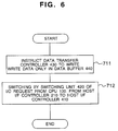
- Fig. 6 is a flow chart illustrating an example of the operation of the external storage system of the embodiment.
- Fig. 7 is a flow chart illustrating an example of the operation of the external storage system of the embodiment.
- Fig. 8 is a flow chart illustrating an example of the operation of the external storage system of the embodiment.
- Fig. 9 is a flow chart illustrating an example of the operation of the external storage system of the embodiment.
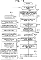
- Fig. 10 is a flow chart illustrating an example of the operation of the external storage system of the embodiment.
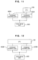
- Fig. 11 illustrates the concept of a modification of interconnection to an upper level system of the external storage system of the embodiment.
- Fig. 12 illustrates the concept of a modification of interconnection to an upper level system of the external storage system of the embodiment.
- Fig. 1 illustrates the concept of an example of a computer system including an external storage sub-system according to an embodiment of the invention.
- the computer system of this embodiment includes an upper level system 100 made of a central processing unit and an external storage sub-system constituted by disk drive controllers 200 and 400 and a disk drive unit 500.
- the disk drive controllers 200 and 400 are connected to the upper level system 100 in a daisy chain form of SCSI interface, and assigned the same SCSIID to configure a redundant structure.
- the disk drive controller 200 in response to a request from the upper system 100, executes a process included in the received request to control the disk drive unit 500, the process being executed also by the redundant disk drive controller 400.
- Fig. 2 is a block diagram showing an example of the internal structures of the disk drive controllers 200 and 400. Both the internal structures of the disk drive controllers 200 and 400 are the same. Therefore, the description will be given for the disk drive controller 200 by way of example and the internal structure of the disk drive controller 400 is omitted by assigning the same lower two digits as the corresponding elements of the disk drive controller 200.
- a microprocessor unit 250 sequentially decodes and executes a microprogram stored in a random access memory (RAM, not shown) to control the whole of the disk drive controller 200.
- a host I/F controller 210 controls protocol used with the upper level system 100.
- a DRV I/F controller 270 controls protocol used with the disk drive unit 500.
- a data buffer 240 is used for data transfer between the host IF controller 210 and DRV I/F controller 270.
- This memory may be a volatile or non-volatile memory. In this embodiment, the following description assumes that the data buffer 240 is a volatile memory.
- a switching unit 220 switches between the host I/F controllers 210 and 410 of the disk drive controllers 200 and 400 to select the host I/F controller which receives I/O from the upper level system 100.
- the host I/F controller 210 receives I/O from the upper level system 100.
- a data transfer controller 230 controls data transfer between the upper level system 100 and a data buffer 240.
- the data transfer controller 230 has both the functions of storing write data from the upper level system 100 into both the data buffers 240 and 440 (hereinafter called "double write”) and storing the write data only in the data buffer 240 (hereinafter called “single write”). It is possible to switch between the double write and single write in accordance with an instruction from MPU 250.
- a DRV transfer controller 260 controls data transfer between the data buffer 240 and disk drive unit 500.
- a communication unit 300 is used for transferring information between MPU 250 and MPU 450. This communication unit 300 can bidirectionally transfer information between MPU 250 and MPU 450.
- a common management memory 310 can be referred to or updated, by both MPU 250 and MPU 450.
- data from the upper level system is distributively stored in a plurality of drives of the disk drive unit 500.
- a disk array will be described illustratively.
- An ECC generator 280 has a function of generating parity data of the data sent from the upper level system 100. This function can be used for recovering data.
- the unit of adding parity data may be a unit of one logic data sent from the upper level or a unit of a plurality of logic data. In this embodiment, parity data is added for each set of four logic data, and is written in conformity with a RAID5 scheme which does not fix a drive in which the parity data is stored.
- Monitor information is used for checking whether each disk drive controller 200/400 operates normally. If it is judged that MPU 250 of the disk drive controller 200 can operate normally, monitor information A321 indicating a normal state is set at a predetermined interval. If it is judged that MPU 250 cannot operate normally, monitor information A321 indicating an abnormal state is set. Similar monitor information B322 to that of MPU 250 is set also for MPU 450 of the disk drive controller 400.
- Data transfer mode information 330 instructs a completion report timing of a write data request from the upper level system 100, during a system degenerate state. Specifically, this information is used for judging whether the timing when the completion report is supplied to the upper level system 100, is at the write completion into the data buffer 240 or 440 (hereinafter called write-after mode) or at the write completion into the disk drive unit 500 from the data buffer 240 (hereinafter called write-through mode).
- Host I/O reception information 340 indicates a disk drive controller 200/400 which receives I/O. In this embodiment, it is assumed that the disk drive controller 200 receives an I/O (input-output) request from the upper level system 100.
- Load distribution information 350 indicates load distribution of a process of an I/O request from the upper level system, into the two disk drive controllers 200 and 400.
- disk drives accessed by each disk drive controller may be assigned to each controller, or a process of an I/O request from the upper level system 100 may be discriminated from a process asynchronous with an I/O request from the upper level system 100 in which write data is asynchronously stored in the disk drive unit 500 from the data buffer.
- all processes of an I/O request are written in the load distribution information to execute the processes by two MPUs.
- the method will be described in which a process of an I/O request from the upper level system 100 is discriminated from a process asynchronous with an I/O request from the upper level system 100 in which write data is asynchronously stored in the disk drive unit 500 from the data buffer 240/440. It is therefore assumed in this embodiment that the load distribution information 350 includes the information on the write data stored in the data buffer 240/440.
- the disk drive controller 200 Upon a write request from the upper level system 100, the disk drive controller 200 receives write data via the host I/F controller 210.
- the data transfer controller 230 stores in duplicate the write data into the data buffers 240 and 440, sets information regarding the write request to the load distribution information 350 of the common management table 310, and at this time reports a completion to the upper level system 100. Thereafter, the disk drive controller 200 can receive the next I/O request from the upper level system.
- the disk drive controller 400 writes the write data received by the disk drive controller 200 from the upper level system into the disk drive unit 500, asynchronously with the processes of the disk drive controller 200.
- MPU 450 refers to the load distribution information 350, and if there is information regarding the write request, reads data (hereinafter called old data) already stored at an address at which the write data is to be written and old parity data for the old data, from the disk drive unit 500 via the DRV I/F controller 470 and DRV transfer controller 460.
- the ECC generator generates parity data (hereinafter called new parity data) of the write data in accordance with the write data, old data, and parity data.
- the generated new parity data and the write data are written into the disk drive unit 500 via the DRV I/F controller 470 and DRV transfer controller 460. In this manner, the write data is stored in the disk drive unit 500.
- the process of reading old data and old parity, the process of generating the new parity data, and the process of storing the new parity data, are called write penalty of RAID5.
- a store request of write data from the upper level system 100 is a process having a very high load if the disk drive unit 500 is used as a disk array. If this process is distributively executed by the two disk drive controllers 200 and 400, the system efficiency and performance can be improved more than when only one disk drive controller is used. Particularly in recent market trend, a very important factor, in addition to high performance and reliability, is to mount an inexpensive processor and reduce the whole system cost. The system performance is degraded by a number of accesses to disk drives during the write penalty process. Rather than this performance degradation, a long run time of microprograms of the microprocessor controlling the write penalty process may often become a bottleneck of the system performance. As in this embodiment, the better performance by about a twofold can be obtained by using the two disk drive controllers 200 and 400.
- MPU 250 Upon a read request from the upper level system 100, MPU 250 starts reading data from the physical drive (disk drive unit 500) via the DRV I/F controller 270 and DRV transfer controller 260, and transfers the read data to the upper level system 100.
- the disk drive controller 400 judges the request as a sequential read process, and may read a predetermined amount of data succeeding the read request address from the data buffers and store it in the data buffers 240 and 440 asynchronously with I/O from the upper level system 100.
- the subject data is already in the data buffers 240 and 440 so that the data can be transferred without any time-consuming access to the disk drive unit 500 and the performance of the whole system can be improved.
- a redundant structure is used, not only reliability but also performance can be improved by making a redundant portion (in this embodiment, the disk drive controller 400) execute part of a process without making it stand by merely as an alternative when a failure occurs.
- MPU 250 sets information indicating a normal state (hereinafter called normal information) to the monitor information 321 whereas MPU 450 sets the normal information to the monitor information 322.
- normal information information sequentially changing is set to the monitor information. For example, information sequentially incremented by 1 may be used.
- abnormal information information indicating an abnormal state (hereinafter called abnormal information) is set to the monitor information.
- MPU 450 of the disk drive controller 400 which monitors the other disk drive controller 200 will be described by way of example.
- MPU 450 judges at Step 600 whether a predetermined time has lapsed. If not lapsed, the flow advances to Step 608 whereat it is judged whether the disk drive controller 200 is normal.
- Step 601 the normal information indicating that MPU 450 is normal, is set.
- Step 602 the monitor information A321 of the disk drive controller 200 is referred to and it is judged whether this information is normal or not at Step 603. If normal, the flow advances to Step 604, whereas if abnormal, the flow advances to Step 607 whereat it is judged that the disk drive controller 200 is in an abnormal state.
- Step 604 the flow advances to Step 604 to compare the normal information with the preceding normal information and at Step 605 it is judged if there is any change in the normal information. Since there is a possibility that MPU 250 cannot set the monitor information because of a failure of microprogram, such a failure is checked at Step 605. If there is any change, the flow advances to Step 608 whereat it is judged to be normal. If there is no change, the flow advances to Step 606 whereat it is judged whether a margin time longer than a predetermined time has lapsed. If lapsed, the flow advances to Step 607 to judge to be abnormal, whereas if not lapsed, the flow advances to Step 608 to judge to be normal. With the above monitor procedure, both the hard ware failure and software failure can be detected.
- the operation of the disk drive controller 400 will be described wherein the controller 400 detects a failure of the other disk drive controller 200 and replaces the controller 200.
- Step 700 MPU 450 sequentially refers to the load distribution information 350. If write data from the upper level system 100 is not stored in the data buffers 240 and 440 at Step 701, the flow advances to Step 704. If write data is stored, the flow advances to Step 702 whereat the old data and old parity corresponding to the write data are read from the disk drive unit 500 so as to generate parity data for the write data stored in the data buffer 440 and the ECC generator 480 generates new parity data. Thereafter, at Step 703, the write data and new parity data are stored in the disk drive unit 500 via the DRV transfer controller 460 and DRV I/F controller 470. Next, at Step 704 it is checked from the monitor procedure at Step 600 and following Steps shown in Fig.
- Step 700 the flow advances to Step 700 to repeat the process. If it is judged that switching is necessary, the flow advances to Step 710 whereat reception of I/O from the upper level system 100 is switched from the disk drive controller 200 to the disk drive controller 400 in accordance with the switching procedure. The I/O process from the upper level system 100 executed by the disk drive controller 200 is switched to the disk drive controller 400 at Step 720.
- Step 711 when write data is received from the upper level system 100, the data transfer controller 430 is instructed to single-write the data in the data buffer 440. Specifically, since the data buffer usable is only in the disk drive controller 400 until the failed disk drive controller 200 is degenerated and disconnected and the defective portion is replaced to recover the normal state, data cannot be double-written as in the normal redundant structure.
- the switching unit 420 instructs to switch the I/O request from the upper level system 100, from the host I/F controller 210 to the host I/F controller 410.
- the host I/F controller 210 does not therefore receive the I/O request from the upper level system 100, but the host I/F controller 410 receives the request from the upper level system 100 so that the disk drive controller is switched substantially.
- the upper level system 100 issues the same SCSIID as before switching of I/O and is not required at all to know the switching of the disk driver controller on the reception side.
- Step 722 After an I/O process is received from the upper level system 100 at Step 721, it is checked at Step 722 whether it is a read request or a write request. If a read request, the data is read from a disk drive of the disk drive unit 500 corresponding to the read request and stored in the data buffer 440 at Step 729. Thereafter, at Step 730 the data is transferred from the data buffer 440 to the upper level system 100 and at Step 728 a completion report is sent to the upper level system 100.
- the write data is stored in the data buffer 440 at Step 723. Thereafter at Step 724 the data transfer mode information 330 is referred to and it is judged at Step 725 whether the mode is a write-through mode. If a write-after mode, i.e., if a completion report to the upper level system 100 is sent at the timing when the data is stored in the data buffer 440, then the flow advances to Step 728 whereat a completion is reported, and at the later time the data in the data buffer 440 is asynchronously stored in the disk drive unit 500.
- a write-after mode i.e., if a completion report to the upper level system 100 is sent at the timing when the data is stored in the data buffer 440, then the flow advances to Step 728 whereat a completion is reported, and at the later time the data in the data buffer 440 is asynchronously stored in the disk drive unit 500.
- Step 726 parity data of the write data is generated at Step 726, the write data and new parity data are stored in the disk drive unit 500 at Step 727, and a completion report is issued at Step 728. Thereafter, Steps 700 to 703 shown in the flow chart of Fig. 5 are executed to execute the process assigned before the switching.
- the disk drive controllers 200 and 400 can be automatically switched and the execution of the process continues, without any instruction from the upper level system 100 and with transparency to the upper level system 100.
- Step 810 the communication unit 300 notifies the disk drive controller 400 of a recovery completion. Thereafter, the disk drive controller 200 becomes a redundant disk drive controller and the roles of the disk drive controllers 200 and 400 are exchanged.
- Step 811 the asynchronous de-stage process (Steps 700 to 705 in Fig. 5) previously executed by the disk drive controller 400 is performed.
- the data transfer controller 430 Upon recognition of the recovery completion of the disk drive controller 200 from the communication unit 300 at Step 820, the data transfer controller 430 is instructed at Step 821 to double-write data into the data buffers 240 and 440.
- Step 822 only the I/O process from the upper level system 100 is executed. In this manner, the original redundant structure can be recovered while receiving the I/O request from the upper level system 100. Furthermore, the load of the process is distributed to the two disk drive controllers 200 and 400 so that the system performance can be improved.
- Step 911 When a request of increasing the capacity of the data buffer is received, it is checked at Step 911 whether the disk drive controller is on the I/O reception side.
- the process at the disk drive controller 200 will be described. Since the disk drive controller 200 is on the I/O reception side, it is first confirmed at Step 912 whether the disk drive controller 400 has been degenerated and disconnected. Then, the data transfer controller 230 is instructed to single-write write data only into the data buffer 240. Thereafter at Step 913 an I/O process from the upper level system 100 is executed, and Steps 700 to 703 shown in Fig. 5 are executed at Step 914. In other words, the process previously executed by the disk drive controller 400 is executed by the disk drive controller 200. While Steps 913 and 914 are repeated, a recovery completion of the disk drive controller 400 is waited for.
- the disk drive controller 400 judges at Step 911 whether the corresponding disk drive controller is on the I/O reception side. Since the disk drive controller 400 is not on the I/O reception side, the disk drive controller 400 is not disconnected and at Step 916 the capacity of the data buffer 440 is increased. After the capacity is increased, a recovery completion is notified at Step 917 via the communication unit 300 to the disk drive controller 200.
- the host I/F controller for receiving I/O is switched at Step 919 to its own by using the switching unit 420 in order for the disk drive controller 400 to receive I/O in place of the disk drive controller 200. Thereafter, the I/O process from the upper level system 100 is executed at Step 920, and Steps 700 to 703 shown in Fig. 5 are executed at Step 921 to wait for the recovery completion of the disk drive controller 200.
- the disk drive controller 200 recognized the recovery at Step 918 via the communication unit 300 is disconnected at Step 922, and the capacity of the data buffer 240 is increased at Step 923. After the capacity is increased, at Step 924 the recovery is notified to the disk drive controller 400 via the communication unit 300. After this notice, since the disk drive controller 200 is not on the host I/O reception side, this controller 200 executes Steps 700 to 705 shown in Fig. 5 at Step 925.
- Step 927 the disk drive controller 400 instructs the data transfer controller 430 to double-write write data both in the data buffers 240 and 440.
- Step 928 an I/O process from the upper level system 100 is executed.
- the capacities of the data buffers 240 and 440 can be increased while I/O from the upper level system 100 is executed.
- the capacities of the data buffers can be increased on line, in contrast to the conventional case where it is not possible unless the system is stopped.
- each board is required to be replaced so that the capacity increase during operation is impossible.
- increasing the capacities of data buffers is possible while each of the disk drive controllers 200 and 400 of a redundant structure is degenerated and recovered.
- Steps 916 and 923 shown in Fig. 10 may be used for exchanging microprograms. Therefore, micro-programs in operation can be replaced and the embodiment is particularly effective for recent computer systems requested for severe 24-hour (around-the-clock) running.
- this data transfer mode information 330 can be automatically performed by a user program. Specifically, if only one data buffer is used, response is excellent if a completion is reported when the data is stored in the data buffer. However, if a failure occurs in the disk drive controller at this time, the data cannot be protected. On the other hand, if the report is made when data is stored in the disk drive controller 500, write penalty processes are required.
- a reliable report can be supplied to the upper level system 100 and reliability is high.
- a user can select as desired either preference for reliability or preference for response speed in accordance with the necessary level of reliability of user files, allowing a flexible file system to be configured.
- the invention can provide a system having a plurality of disk drive controllers of a redundant structure which are not only redundant but also accessible at the same time via a plurality of upper level systems or busses. Examples of the structure of such a system are shown in Figs. 11 and 12.
- Fig. 11 has the same structure as the system described previously. However, if I/F to the upper level system 100 is SCSI, the structure shown in Fig. 1 uses the same SCSIID shared by both storage controllers 0 and 1 whereas the structure shown in Fig. 11 uses different SCSIIDs for the storage controller 0 (400A) and storage controller 1 (200A). In the structure shown in Fig. 11, both the storage controllers receive an I/O request from the same upper level system 100.
- Fig. 12 is a block diagram showing an example of the system structure in which a plurality of storage controllers 0 (400B) and 1 (200B) are connected via multi-buses to the same upper level system 100. Also in this structure shown in Fig.
- the storage controllers 0 (400B) and 1 (200B) can execute an I/O request from the upper level system 100.
- Designation of which one of the storage controllers executes an I/O request is realized by changing the contents of the host I/O reception information 340 of the common management table 310.
- each storage controller refers to the host I/O reception information 340 to determine whether or not it receives the I/O request from the upper level system.
- this invention can deal with various interconnections user desires and can configure flexible systems.
- a plurality of disk drive controllers 200 and 400 of a redundant structure can execute a request from the upper level system 100 while distributing the load. It is therefore possible to provide a file system with not only improved reliability but also improved performance. Further, while all the disk drive controllers 200 and 400 execute an I/O request from the upper level system 100 by distributing the load, the operation continues even upon occurrence of a failure through automatic switching without any instruction from the upper level system 100, and the normal state can be retrieved. Accordingly, while an I/O request from the upper level system 100 is executed, increasing the capacity of data buffers or exchanging microprograms can be performed so that uninterrupted operation can be achieved. All disk drive controllers can be configured not only to be redundant but also to receive a request from the upper level system 100 at the same time. Therefore, various types of file systems users desire can be dealt with flexibly.
- a load is distributed into a plurality of storage controllers of a redundant structure. Therefore, advantageous effects of improved reliability and performance can be obtained.
Landscapes
- Engineering & Computer Science (AREA)
- Theoretical Computer Science (AREA)
- General Engineering & Computer Science (AREA)
- Physics & Mathematics (AREA)
- General Physics & Mathematics (AREA)
- Human Computer Interaction (AREA)
- Quality & Reliability (AREA)
- Computer Networks & Wireless Communication (AREA)
- Computer Hardware Design (AREA)
- Techniques For Improving Reliability Of Storages (AREA)
- Information Retrieval, Db Structures And Fs Structures Therefor (AREA)
- Hardware Redundancy (AREA)
Applications Claiming Priority (3)
| Application Number | Priority Date | Filing Date | Title |
|---|---|---|---|
| JP139781/95 | 1995-06-07 | ||
| JP13978195A JP3732869B2 (ja) | 1995-06-07 | 1995-06-07 | 外部記憶装置 |
| JP13978195 | 1995-06-07 |
Publications (3)
| Publication Number | Publication Date |
|---|---|
| EP0747822A2 true EP0747822A2 (fr) | 1996-12-11 |
| EP0747822A3 EP0747822A3 (fr) | 1997-04-09 |
| EP0747822B1 EP0747822B1 (fr) | 2001-10-04 |
Family
ID=15253279
Family Applications (1)
| Application Number | Title | Priority Date | Filing Date |
|---|---|---|---|
| EP96109061A Expired - Lifetime EP0747822B1 (fr) | 1995-06-07 | 1996-06-05 | Système de mémoire externe avec contrôleurs de mémoire redondants |
Country Status (4)
| Country | Link |
|---|---|
| US (1) | US5720028A (fr) |
| EP (1) | EP0747822B1 (fr) |
| JP (1) | JP3732869B2 (fr) |
| DE (1) | DE69615611T2 (fr) |
Cited By (17)
| Publication number | Priority date | Publication date | Assignee | Title |
|---|---|---|---|---|
| EP0772127A1 (fr) * | 1995-10-30 | 1997-05-07 | Hitachi, Ltd. | Rétablissement de défaillance de contrÔleur dans une mémoire externe |
| EP0889409A1 (fr) * | 1997-06-26 | 1999-01-07 | Digital Equipment Corporation | Echange sous tension d'un module antémémoire à postmémorisation reflété |
| EP0889410A3 (fr) * | 1997-06-26 | 1999-01-13 | Sun Microsystems, Inc. | Procédé et appareil pour dispositifs de stockage de données à haute disponibilité et avec cache |
| WO1999063438A1 (fr) * | 1998-06-05 | 1999-12-09 | Mylex Corporation | Appareil, systeme et procede destine a une unite de commande de matrice redondante a disques independants a n voies |
| US6931567B2 (en) | 2000-01-31 | 2005-08-16 | Hitachi, Ltd. | Storage system |
| EP1372076A3 (fr) * | 2002-06-14 | 2006-08-16 | Hitachi Ltd. | Système de commande de mémoire et procédé d'utilisation |
| EP0990988A3 (fr) * | 1998-09-28 | 2006-10-25 | Hitachi, Ltd. | Unité de commande pour une mémoire de données et méthode de traitement d'une système de stockage de données |
| JP2007199891A (ja) * | 2006-01-25 | 2007-08-09 | Hitachi Ltd | ストレージシステム及び記憶制御装置 |
| WO2008070799A3 (fr) * | 2006-12-06 | 2008-10-23 | David Flynn | Appareil, système et procédé pour fournir des demandes d'objet dans des unités de commande de mémorisation |
| US8151082B2 (en) | 2007-12-06 | 2012-04-03 | Fusion-Io, Inc. | Apparatus, system, and method for converting a storage request into an append data storage command |
| US8161353B2 (en) | 2007-12-06 | 2012-04-17 | Fusion-Io, Inc. | Apparatus, system, and method for validating that a correct data segment is read from a data storage device |
| WO2012164625A1 (fr) * | 2011-06-01 | 2012-12-06 | Hitachi, Ltd. | Système de stockage à répartition de charge et procédé associé |
| CN101636712B (zh) * | 2006-12-06 | 2016-04-13 | 才智知识产权控股公司(2) | 在存储控制器内服务对象请求的装置、系统和方法 |
| US9767017B2 (en) | 2010-12-13 | 2017-09-19 | Sandisk Technologies Llc | Memory device with volatile and non-volatile media |
| US10009438B2 (en) | 2015-05-20 | 2018-06-26 | Sandisk Technologies Llc | Transaction log acceleration |
| US10817502B2 (en) | 2010-12-13 | 2020-10-27 | Sandisk Technologies Llc | Persistent memory management |
| US10817421B2 (en) | 2010-12-13 | 2020-10-27 | Sandisk Technologies Llc | Persistent data structures |
Families Citing this family (71)
| Publication number | Priority date | Publication date | Assignee | Title |
|---|---|---|---|---|
| US6009535A (en) * | 1997-06-30 | 1999-12-28 | Emc Corporation | SCSI adaptor failover for a disk drive system |
| JPH1185659A (ja) | 1997-09-03 | 1999-03-30 | Hitachi Ltd | ディスク制御装置及びこれを用いた記憶装置 |
| US6349357B1 (en) | 1999-03-04 | 2002-02-19 | Sun Microsystems, Inc. | Storage architecture providing scalable performance through independent control and data transfer paths |
| US6397267B1 (en) * | 1999-03-04 | 2002-05-28 | Sun Microsystems, Inc. | Redirected I/O for scalable performance storage architecture |
| US6370605B1 (en) | 1999-03-04 | 2002-04-09 | Sun Microsystems, Inc. | Switch based scalable performance storage architecture |
| US6616819B1 (en) * | 1999-11-04 | 2003-09-09 | Therasense, Inc. | Small volume in vitro analyte sensor and methods |
| US6604155B1 (en) | 1999-11-09 | 2003-08-05 | Sun Microsystems, Inc. | Storage architecture employing a transfer node to achieve scalable performance |
| US6598106B1 (en) | 1999-12-23 | 2003-07-22 | Lsi Logic Corporation | Dual-port SCSI sub-system with fail-over capabilities |
| US6574753B1 (en) * | 2000-01-10 | 2003-06-03 | Emc Corporation | Peer link fault isolation |
| US7228538B1 (en) | 2000-05-02 | 2007-06-05 | International Business Machines Corporation | Method, system, and program for updating firmware to a storage system comprised of multiple controllers |
| US6393535B1 (en) | 2000-05-02 | 2002-05-21 | International Business Machines Corporation | Method, system, and program for modifying preferred path assignments to a storage device |
| US6601128B1 (en) | 2000-05-02 | 2003-07-29 | International Business Machines Corporation | Method, system, program, and data structure for selecting a preferred path to a storage device |
| JP2002236682A (ja) * | 2001-02-13 | 2002-08-23 | Fuji Photo Film Co Ltd | データベース・システム |
| JP4060552B2 (ja) * | 2001-08-06 | 2008-03-12 | 株式会社日立製作所 | 記憶装置システム、および、記憶装置システムの構成方法 |
| JP4721379B2 (ja) * | 2001-09-26 | 2011-07-13 | 株式会社日立製作所 | ストレージシステム、ディスク制御クラスタおよびディスク制御クラスタの増設方法 |
| JP3800516B2 (ja) * | 2002-01-22 | 2006-07-26 | インターナショナル・ビジネス・マシーンズ・コーポレーション | 外部記憶装置、制御方法、外部記憶装置システム、プログラム、及び記録媒体 |
| JP4219602B2 (ja) | 2002-03-01 | 2009-02-04 | 株式会社日立製作所 | 記憶制御装置および記憶制御装置の制御方法 |
| JPWO2003075161A1 (ja) * | 2002-03-07 | 2005-06-30 | 富士通株式会社 | ストレージ仮想化システムの変換管理装置およびストレージ仮想化システムの変換管理方法 |
| US6934878B2 (en) * | 2002-03-22 | 2005-08-23 | Intel Corporation | Failure detection and failure handling in cluster controller networks |
| JP2003316522A (ja) * | 2002-04-26 | 2003-11-07 | Hitachi Ltd | 計算機システムおよび計算機システムの制御方法 |
| US6859890B2 (en) * | 2002-04-30 | 2005-02-22 | Lsi Logic Corporation | Method for reducing data/parity inconsistencies due to a storage controller failure |
| JP2004171437A (ja) | 2002-11-22 | 2004-06-17 | Fujitsu Ltd | ストレージ制御装置及びその制御方法 |
| JP2004234555A (ja) * | 2003-01-31 | 2004-08-19 | Hitachi Ltd | ストレージシステムの制御方法、ストレージシステム、及びプログラム |
| JP4342804B2 (ja) * | 2003-01-31 | 2009-10-14 | 株式会社日立製作所 | ストレージシステムの制御方法、ストレージシステム、及びプログラム |
| JP2004234558A (ja) * | 2003-01-31 | 2004-08-19 | Hitachi Ltd | 記憶デバイス制御装置、及びプログラム |
| US20040168008A1 (en) * | 2003-02-18 | 2004-08-26 | Hewlett-Packard Development Company, L.P. | High speed multiple ported bus interface port state identification system |
| US20040162928A1 (en) * | 2003-02-18 | 2004-08-19 | Hewlett-Packard Development Company, L.P. | High speed multiple ported bus interface reset control system |
| JP2004302713A (ja) * | 2003-03-31 | 2004-10-28 | Hitachi Ltd | 記憶システム及びその制御方法 |
| JP4090400B2 (ja) * | 2003-07-24 | 2008-05-28 | 株式会社日立製作所 | ストレージシステム |
| JP4386694B2 (ja) * | 2003-09-16 | 2009-12-16 | 株式会社日立製作所 | 記憶システム及び記憶制御装置 |
| US7725760B2 (en) * | 2003-09-23 | 2010-05-25 | Symantec Operating Corporation | Data storage system |
| US7287133B2 (en) | 2004-08-24 | 2007-10-23 | Symantec Operating Corporation | Systems and methods for providing a modification history for a location within a data store |
| US7577806B2 (en) | 2003-09-23 | 2009-08-18 | Symantec Operating Corporation | Systems and methods for time dependent data storage and recovery |
| US7730222B2 (en) | 2004-08-24 | 2010-06-01 | Symantec Operating System | Processing storage-related I/O requests using binary tree data structures |
| US7577807B2 (en) * | 2003-09-23 | 2009-08-18 | Symantec Operating Corporation | Methods and devices for restoring a portion of a data store |
| US7904428B2 (en) * | 2003-09-23 | 2011-03-08 | Symantec Corporation | Methods and apparatus for recording write requests directed to a data store |
| US7827362B2 (en) * | 2004-08-24 | 2010-11-02 | Symantec Corporation | Systems, apparatus, and methods for processing I/O requests |
| US7991748B2 (en) * | 2003-09-23 | 2011-08-02 | Symantec Corporation | Virtual data store creation and use |
| US7631120B2 (en) | 2004-08-24 | 2009-12-08 | Symantec Operating Corporation | Methods and apparatus for optimally selecting a storage buffer for the storage of data |
| JP2005165852A (ja) | 2003-12-04 | 2005-06-23 | Hitachi Ltd | ストレージシステム、ストレージ制御装置、ストレージシステムの制御方法 |
| US7549029B2 (en) * | 2005-05-06 | 2009-06-16 | International Business Machines Corporation | Methods for creating hierarchical copies |
| JP4327130B2 (ja) * | 2005-06-24 | 2009-09-09 | 富士通株式会社 | ディスクアレイアクセス動的制御装置、及び方法 |
| JP4806557B2 (ja) * | 2005-10-18 | 2011-11-02 | 株式会社日立製作所 | ログを管理するストレージ装置及び計算機システム |
| JP2007219571A (ja) | 2006-02-14 | 2007-08-30 | Hitachi Ltd | 記憶制御装置及びストレージシステム |
| JP4901316B2 (ja) * | 2006-06-06 | 2012-03-21 | 株式会社日立製作所 | ストレージシステム及び記憶制御装置 |
| US20080005382A1 (en) * | 2006-06-14 | 2008-01-03 | Hitachi, Ltd. | System and method for resource allocation in fault tolerant storage system |
| US9116823B2 (en) | 2006-12-06 | 2015-08-25 | Intelligent Intellectual Property Holdings 2 Llc | Systems and methods for adaptive error-correction coding |
| US9495241B2 (en) | 2006-12-06 | 2016-11-15 | Longitude Enterprise Flash S.A.R.L. | Systems and methods for adaptive data storage |
| JP5106913B2 (ja) * | 2007-04-23 | 2012-12-26 | 株式会社日立製作所 | ストレージシステム、ストレージシステム管理方法、及び計算機システム |
| US8150806B2 (en) * | 2007-09-11 | 2012-04-03 | International Business Machines Corporation | Idempotent storage replication management |
| US8195912B2 (en) | 2007-12-06 | 2012-06-05 | Fusion-io, Inc | Apparatus, system, and method for efficient mapping of virtual and physical addresses |
| US9519540B2 (en) | 2007-12-06 | 2016-12-13 | Sandisk Technologies Llc | Apparatus, system, and method for destaging cached data |
| US7836226B2 (en) | 2007-12-06 | 2010-11-16 | Fusion-Io, Inc. | Apparatus, system, and method for coordinating storage requests in a multi-processor/multi-thread environment |
| US9300738B2 (en) * | 2008-01-03 | 2016-03-29 | International Business Machines Corporation | Virtual state machine for managing operation requests in a client server environment |
| JP2009230484A (ja) * | 2008-03-24 | 2009-10-08 | Nec Corp | ストレージサブシステム、ストレージシステム、ファームウェア置換方法、及びプログラム |
| JP5183403B2 (ja) * | 2008-09-30 | 2013-04-17 | 株式会社日立製作所 | ストレージシステムおよび制御プログラムならびにストレージシステム制御方法 |
| US8346996B2 (en) | 2008-10-29 | 2013-01-01 | Nec Corporation | Information processing system |
| US9223514B2 (en) | 2009-09-09 | 2015-12-29 | SanDisk Technologies, Inc. | Erase suspend/resume for memory |
| US8429436B2 (en) | 2009-09-09 | 2013-04-23 | Fusion-Io, Inc. | Apparatus, system, and method for power reduction in a storage device |
| US8321622B2 (en) * | 2009-11-10 | 2012-11-27 | Hitachi, Ltd. | Storage system with multiple controllers and multiple processing paths |
| US8984216B2 (en) | 2010-09-09 | 2015-03-17 | Fusion-Io, Llc | Apparatus, system, and method for managing lifetime of a storage device |
| CN103262054B (zh) | 2010-12-13 | 2015-11-25 | 桑迪士克科技股份有限公司 | 用于自动提交存储器的装置、系统和方法 |
| US9218278B2 (en) | 2010-12-13 | 2015-12-22 | SanDisk Technologies, Inc. | Auto-commit memory |
| US9047178B2 (en) | 2010-12-13 | 2015-06-02 | SanDisk Technologies, Inc. | Auto-commit memory synchronization |
| WO2012116369A2 (fr) | 2011-02-25 | 2012-08-30 | Fusion-Io, Inc. | Appareil, système et procédé de gestion du contenu d'une antémémoire |
| US9021232B2 (en) * | 2011-06-30 | 2015-04-28 | Infinidat Ltd. | Multipath storage system and method of operating thereof |
| WO2013013282A1 (fr) * | 2011-07-22 | 2013-01-31 | HYDRO-QUéBEC | Appareil de commutation, système de commande et procédé de modification d'impédance de ligne de phase |
| US9251086B2 (en) | 2012-01-24 | 2016-02-02 | SanDisk Technologies, Inc. | Apparatus, system, and method for managing a cache |
| JP6750380B2 (ja) | 2016-08-05 | 2020-09-02 | 富士通株式会社 | 制御装置、ストレージ装置、及び制御プログラム |
| WO2018173246A1 (fr) * | 2017-03-24 | 2018-09-27 | 株式会社日立製作所 | Système de mémoire et procédé de commande de mémoire |
| US10558598B2 (en) * | 2018-03-20 | 2020-02-11 | Seagate Technology Llc | Logic circuit that provides verification of signals used to interrupt server operation |
Family Cites Families (13)
| Publication number | Priority date | Publication date | Assignee | Title |
|---|---|---|---|---|
| JPS63178360A (ja) * | 1987-01-20 | 1988-07-22 | Hitachi Ltd | 入出力システム構成方式 |
| JPH03206529A (ja) * | 1990-01-09 | 1991-09-09 | Fujitsu Ltd | コンピュータシステム |
| US5140592A (en) * | 1990-03-02 | 1992-08-18 | Sf2 Corporation | Disk array system |
| JPH04628A (ja) * | 1990-04-18 | 1992-01-06 | Nec Corp | サブシステム構成の認識方法 |
| US5274799A (en) * | 1991-01-04 | 1993-12-28 | Array Technology Corporation | Storage device array architecture with copyback cache |
| WO1992018931A1 (fr) * | 1991-04-23 | 1992-10-29 | Eastman Kodak Company | Systeme de fichier pour reseau insensible aux defaillances |
| US5313584A (en) * | 1991-11-25 | 1994-05-17 | Unisys Corporation | Multiple I/O processor system |
| WO1993018456A1 (fr) * | 1992-03-13 | 1993-09-16 | Emc Corporation | Partage d'une unite de controle multiple dans un systeme d'unites de stockage redondant |
| JP2999089B2 (ja) * | 1993-05-10 | 2000-01-17 | 株式会社日立製作所 | 通信制御装置の2重化システム |
| JP3004861U (ja) * | 1993-06-04 | 1994-11-29 | ディジタル イクイプメント コーポレイション | 密接に結合された二重のコントローラモジュールを用いた欠陥許容式の記憶装置用制御システム |
| US5548711A (en) * | 1993-08-26 | 1996-08-20 | Emc Corporation | Method and apparatus for fault tolerant fast writes through buffer dumping |
| US5504882A (en) * | 1994-06-20 | 1996-04-02 | International Business Machines Corporation | Fault tolerant data storage subsystem employing hierarchically arranged controllers |
| US5588110A (en) * | 1995-05-23 | 1996-12-24 | Symbios Logic Inc. | Method for transferring data between two devices that insures data recovery in the event of a fault |
-
1995
- 1995-06-07 JP JP13978195A patent/JP3732869B2/ja not_active Expired - Fee Related
-
1996
- 1996-06-05 US US08/660,685 patent/US5720028A/en not_active Expired - Lifetime
- 1996-06-05 DE DE69615611T patent/DE69615611T2/de not_active Expired - Lifetime
- 1996-06-05 EP EP96109061A patent/EP0747822B1/fr not_active Expired - Lifetime
Cited By (32)
| Publication number | Priority date | Publication date | Assignee | Title |
|---|---|---|---|---|
| EP0772127A1 (fr) * | 1995-10-30 | 1997-05-07 | Hitachi, Ltd. | Rétablissement de défaillance de contrÔleur dans une mémoire externe |
| US6052795A (en) * | 1995-10-30 | 2000-04-18 | Hitachi, Ltd. | Recovery method and system for continued I/O processing upon a controller failure |
| US6412078B2 (en) | 1995-10-30 | 2002-06-25 | Hitachi, Ltd. | External storage |
| EP0889409A1 (fr) * | 1997-06-26 | 1999-01-07 | Digital Equipment Corporation | Echange sous tension d'un module antémémoire à postmémorisation reflété |
| EP0889410A3 (fr) * | 1997-06-26 | 1999-01-13 | Sun Microsystems, Inc. | Procédé et appareil pour dispositifs de stockage de données à haute disponibilité et avec cache |
| US6070251A (en) * | 1997-06-26 | 2000-05-30 | Sun Microsystems, Inc. | Method and apparatus for high availability and caching data storage devices |
| WO1999063438A1 (fr) * | 1998-06-05 | 1999-12-09 | Mylex Corporation | Appareil, systeme et procede destine a une unite de commande de matrice redondante a disques independants a n voies |
| US6601138B2 (en) | 1998-06-05 | 2003-07-29 | International Business Machines Corporation | Apparatus system and method for N-way RAID controller having improved performance and fault tolerance |
| EP0990988A3 (fr) * | 1998-09-28 | 2006-10-25 | Hitachi, Ltd. | Unité de commande pour une mémoire de données et méthode de traitement d'une système de stockage de données |
| US6931567B2 (en) | 2000-01-31 | 2005-08-16 | Hitachi, Ltd. | Storage system |
| EP1372076A3 (fr) * | 2002-06-14 | 2006-08-16 | Hitachi Ltd. | Système de commande de mémoire et procédé d'utilisation |
| US7650462B2 (en) | 2006-01-25 | 2010-01-19 | Hitachi, Ltd. | Storage system and storage control apparatuses with compression and load balancing |
| JP2007199891A (ja) * | 2006-01-25 | 2007-08-09 | Hitachi Ltd | ストレージシステム及び記憶制御装置 |
| EP1818798A3 (fr) * | 2006-01-25 | 2009-08-05 | Hitachi, Ltd. | Système de stockage et appareil de contrôle de stockage |
| US11960412B2 (en) | 2006-12-06 | 2024-04-16 | Unification Technologies Llc | Systems and methods for identifying storage resources that are not in use |
| WO2008070799A3 (fr) * | 2006-12-06 | 2008-10-23 | David Flynn | Appareil, système et procédé pour fournir des demandes d'objet dans des unités de commande de mémorisation |
| US11573909B2 (en) | 2006-12-06 | 2023-02-07 | Unification Technologies Llc | Apparatus, system, and method for managing commands of solid-state storage using bank interleave |
| US11847066B2 (en) | 2006-12-06 | 2023-12-19 | Unification Technologies Llc | Apparatus, system, and method for managing commands of solid-state storage using bank interleave |
| US8402201B2 (en) | 2006-12-06 | 2013-03-19 | Fusion-Io, Inc. | Apparatus, system, and method for storage space recovery in solid-state storage |
| US11640359B2 (en) | 2006-12-06 | 2023-05-02 | Unification Technologies Llc | Systems and methods for identifying storage resources that are not in use |
| CN101636712B (zh) * | 2006-12-06 | 2016-04-13 | 才智知识产权控股公司(2) | 在存储控制器内服务对象请求的装置、系统和方法 |
| US9734086B2 (en) | 2006-12-06 | 2017-08-15 | Sandisk Technologies Llc | Apparatus, system, and method for a device shared between multiple independent hosts |
| US8161353B2 (en) | 2007-12-06 | 2012-04-17 | Fusion-Io, Inc. | Apparatus, system, and method for validating that a correct data segment is read from a data storage device |
| US8151082B2 (en) | 2007-12-06 | 2012-04-03 | Fusion-Io, Inc. | Apparatus, system, and method for converting a storage request into an append data storage command |
| US9772938B2 (en) | 2010-12-13 | 2017-09-26 | Sandisk Technologies Llc | Auto-commit memory metadata and resetting the metadata by writing to special address in free space of page storing the metadata |
| US10817502B2 (en) | 2010-12-13 | 2020-10-27 | Sandisk Technologies Llc | Persistent memory management |
| US10817421B2 (en) | 2010-12-13 | 2020-10-27 | Sandisk Technologies Llc | Persistent data structures |
| US9767017B2 (en) | 2010-12-13 | 2017-09-19 | Sandisk Technologies Llc | Memory device with volatile and non-volatile media |
| US8756381B2 (en) | 2011-06-01 | 2014-06-17 | Hitachi, Ltd. | Storage subsystem and load distribution method for executing data processing using normal resources even if an abnormality occurs in part of the data processing resources that intermediate data processing between a host computer and a storage device |
| WO2012164625A1 (fr) * | 2011-06-01 | 2012-12-06 | Hitachi, Ltd. | Système de stockage à répartition de charge et procédé associé |
| US10009438B2 (en) | 2015-05-20 | 2018-06-26 | Sandisk Technologies Llc | Transaction log acceleration |
| US10834224B2 (en) | 2015-05-20 | 2020-11-10 | Sandisk Technologies Llc | Transaction log acceleration |
Also Published As
| Publication number | Publication date |
|---|---|
| EP0747822B1 (fr) | 2001-10-04 |
| EP0747822A3 (fr) | 1997-04-09 |
| DE69615611T2 (de) | 2002-05-29 |
| US5720028A (en) | 1998-02-17 |
| JP3732869B2 (ja) | 2006-01-11 |
| DE69615611D1 (de) | 2001-11-08 |
| JPH08335144A (ja) | 1996-12-17 |
Similar Documents
| Publication | Publication Date | Title |
|---|---|---|
| US5720028A (en) | External storage system | |
| JP3772369B2 (ja) | 記憶サブシステム | |
| US7133967B2 (en) | Storage system, controller, control method and program product therefor | |
| US8423818B2 (en) | Disk array apparatus and method for controlling the same | |
| US5740397A (en) | IDE disk drive adapter for computer backup and fault tolerance | |
| EP0760503B1 (fr) | Serveurs de réseau multiples à tolérance de fautes. | |
| US6052797A (en) | Remotely mirrored data storage system with a count indicative of data consistency | |
| US6044444A (en) | Remote data mirroring having preselection of automatic recovery or intervention required when a disruption is detected | |
| US7962783B2 (en) | Preventing write corruption in a raid array | |
| US6425049B1 (en) | Disk array system and method of changing the configuration of the disk array system | |
| US7398367B2 (en) | Storage subsystem that connects fibre channel and supports online backup | |
| US6009535A (en) | SCSI adaptor failover for a disk drive system | |
| US6961818B1 (en) | Method, system and computer program product for managing data in a mirrored cache using an access balancing technique | |
| US6438647B1 (en) | Method and apparatus for providing battery-backed immediate write back cache for an array of disk drives in a computer system | |
| WO1992015057A1 (fr) | Calcul de parite dans un ensemble efficace de dispositifs de memoire de masse | |
| KR20020025759A (ko) | 디스크 어레이 장치, 그 장치에 대한 에러 제어 방법, 및그 방법에 대한 제어 프로그램 | |
| JP2004199551A (ja) | ストレージシステム及び障害ストレージ装置の切り離し方法 | |
| US6804794B1 (en) | Error condition handling | |
| JPH09269871A (ja) | ディスクアレイ装置におけるデータ再冗長化方式 | |
| JP3776438B2 (ja) | 記憶装置 | |
| US6687852B1 (en) | Ultra reliable disk memory for duplex processor platforms | |
| JP2006114064A (ja) | 記憶サブシステム | |
| US6671823B1 (en) | Ultra reliable disk memory for multi-processor platforms | |
| JP3050169B2 (ja) | ディスクアレイシステム | |
| JP2002007220A (ja) | 多重化メモリシステム |
Legal Events
| Date | Code | Title | Description |
|---|---|---|---|
| PUAI | Public reference made under article 153(3) epc to a published international application that has entered the european phase |
Free format text: ORIGINAL CODE: 0009012 |
|
| AK | Designated contracting states |
Kind code of ref document: A2 Designated state(s): DE FR GB |
|
| PUAL | Search report despatched |
Free format text: ORIGINAL CODE: 0009013 |
|
| AK | Designated contracting states |
Kind code of ref document: A3 Designated state(s): DE FR GB |
|
| 17P | Request for examination filed |
Effective date: 19970923 |
|
| 17Q | First examination report despatched |
Effective date: 19980527 |
|
| GRAG | Despatch of communication of intention to grant |
Free format text: ORIGINAL CODE: EPIDOS AGRA |
|
| GRAG | Despatch of communication of intention to grant |
Free format text: ORIGINAL CODE: EPIDOS AGRA |
|
| GRAG | Despatch of communication of intention to grant |
Free format text: ORIGINAL CODE: EPIDOS AGRA |
|
| GRAH | Despatch of communication of intention to grant a patent |
Free format text: ORIGINAL CODE: EPIDOS IGRA |
|
| GRAH | Despatch of communication of intention to grant a patent |
Free format text: ORIGINAL CODE: EPIDOS IGRA |
|
| GRAA | (expected) grant |
Free format text: ORIGINAL CODE: 0009210 |
|
| AK | Designated contracting states |
Kind code of ref document: B1 Designated state(s): DE FR GB |
|
| REF | Corresponds to: |
Ref document number: 69615611 Country of ref document: DE Date of ref document: 20011108 |
|
| REG | Reference to a national code |
Ref country code: GB Ref legal event code: IF02 |
|
| ET | Fr: translation filed | ||
| PLBE | No opposition filed within time limit |
Free format text: ORIGINAL CODE: 0009261 |
|
| STAA | Information on the status of an ep patent application or granted ep patent |
Free format text: STATUS: NO OPPOSITION FILED WITHIN TIME LIMIT |
|
| 26N | No opposition filed | ||
| PGFP | Annual fee paid to national office [announced via postgrant information from national office to epo] |
Ref country code: DE Payment date: 20120530 Year of fee payment: 17 |
|
| PGFP | Annual fee paid to national office [announced via postgrant information from national office to epo] |
Ref country code: GB Payment date: 20120530 Year of fee payment: 17 Ref country code: FR Payment date: 20120619 Year of fee payment: 17 |
|
| GBPC | Gb: european patent ceased through non-payment of renewal fee |
Effective date: 20130605 |
|
| REG | Reference to a national code |
Ref country code: DE Ref legal event code: R119 Ref document number: 69615611 Country of ref document: DE Effective date: 20140101 |
|
| REG | Reference to a national code |
Ref country code: FR Ref legal event code: ST Effective date: 20140228 |
|
| PG25 | Lapsed in a contracting state [announced via postgrant information from national office to epo] |
Ref country code: GB Free format text: LAPSE BECAUSE OF NON-PAYMENT OF DUE FEES Effective date: 20130605 Ref country code: DE Free format text: LAPSE BECAUSE OF NON-PAYMENT OF DUE FEES Effective date: 20140101 |
|
| PG25 | Lapsed in a contracting state [announced via postgrant information from national office to epo] |
Ref country code: FR Free format text: LAPSE BECAUSE OF NON-PAYMENT OF DUE FEES Effective date: 20130701 |