EP0749089A2 - Circuit pour transférer des données vers une tête d'impression - Google Patents
Circuit pour transférer des données vers une tête d'impression Download PDFInfo
- Publication number
- EP0749089A2 EP0749089A2 EP96102645A EP96102645A EP0749089A2 EP 0749089 A2 EP0749089 A2 EP 0749089A2 EP 96102645 A EP96102645 A EP 96102645A EP 96102645 A EP96102645 A EP 96102645A EP 0749089 A2 EP0749089 A2 EP 0749089A2
- Authority
- EP
- European Patent Office
- Prior art keywords
- data
- input
- register
- clock
- flop
- Prior art date
- Legal status (The legal status is an assumption and is not a legal conclusion. Google has not performed a legal analysis and makes no representation as to the accuracy of the status listed.)
- Withdrawn
Links
Images

Classifications
-
- G—PHYSICS
- G06—COMPUTING OR CALCULATING; COUNTING
- G06K—GRAPHICAL DATA READING; PRESENTATION OF DATA; RECORD CARRIERS; HANDLING RECORD CARRIERS
- G06K15/00—Arrangements for producing a permanent visual presentation of the output data, e.g. computer output printers
- G06K15/02—Arrangements for producing a permanent visual presentation of the output data, e.g. computer output printers using printers
- G06K15/10—Arrangements for producing a permanent visual presentation of the output data, e.g. computer output printers using printers by matrix printers
-
- G—PHYSICS
- G06—COMPUTING OR CALCULATING; COUNTING
- G06K—GRAPHICAL DATA READING; PRESENTATION OF DATA; RECORD CARRIERS; HANDLING RECORD CARRIERS
- G06K2215/00—Arrangements for producing a permanent visual presentation of the output data
- G06K2215/0002—Handling the output data
- G06K2215/0077—Raster outputting to the print element(s)
Definitions
- the invention relates to a circuit for transferring data to a print head according to the preambles of claims 1 and 4.
- printheads - in particular thermal printheads - transmit the data to be printed out in serial form.
- Each print line to be transferred to a recording medium is converted into serial form by data word and is transferred via a data line, ie a cable, from the main board of the printer to the data input of a register attached directly to the thermal print head.
- a data line ie a cable
- the actual printing process takes place; the heating elements are activated according to the data stored in the register.
- a second cable, the synchronization line is used to synchronize the data transmission.
- Individual data are transferred from the data input to the register if and only if the state of the clock input connected to the synchronization line changes from zero One (or alternatively from one to zero) changes.
- the data contained in the register are shifted one memory cell at a time. After a number of synchronization pulses, which corresponds to the number of memory cells in the register, all memory cells are filled and the printing process is carried out.
- a disadvantage here is that the physical properties of the lines can lead to data transmission errors. Since the output resistances of conventional circuits are much higher than the characteristic impedances of the cables, it is not possible to correctly adapt the input and output resistances of the circuits used to the cables. The mismatch creates undesirable reflections at the data and clock input of the printhead, which are noticeable by exponentially decaying vibrations at the reversal points of the originally rectangular signals. It is therefore sometimes no longer possible to distinguish whether the signal at the data input is now zero or one. The disadvantageous consequence is errors in the printed image.
- the object of the present invention is to provide a circuit of the generic type which is distinguished by fast and low-error transmission of data to be printed out to the print head.
- the object is achieved in that the signals at the clock input are delayed in phase by a fixed phase angle compared to the signals at the data input.
- the main idea is to only apply a signal to the clock input when the unwanted vibrations at the data input caused by reflections have subsided. Since the clock input is delayed, i.e. phase-shifted, signals is applied, the rising or falling edge of the synchronization signal arrives only after a time-constant signal that is no longer affected by the reflections is present at the data input of the register, so that data errors are no longer possible.
- the advantages of the invention consist primarily in the fact that errors in the transmission of data to the printhead caused by reflections are no longer to be feared.
- the control circuit according to the invention is inexpensive, inexpensive to implement and reliable. It also makes it possible to increase the speed of data transmission with a reduced error rate.
- the invention can be implemented in a manner known per se by means of a parallel-serial converter.
- the latter is loaded by the microprocessor with the data to be printed out, word by word, via a data bus.
- a rectangular synchronization signal is present at a clock input of the converter, which controls the serial transmission of the data - via the data line - to the print head.
- the synchronization signal is still shifted in phase and placed on the clock input of the printhead.
- the phase shift can take place on the main circuit board of the printer or directly on the printhead and can take place, for example, by means of a low-pass filter (RC element).
- RC element low-pass filter
- the error rate of data transmission in a circuit for transmitting data to a printhead in which the data are brought into serial form by means of a parallel-serial converter and via a data line to a data input associated with the printhead Registers are transmitted, wherein a synchronization signal is applied to a clock input of the parallel-serial converter
- a flip-flop is present, in which an input state appears delayed by a clock signal at an output, that the output of the flip-flop with is connected to the data input of the register, that a data input of the flip-flop is connected to the output of the parallel-serial converter, that the output signal of an oscillator is halved in frequency and applied to the clock input of the parallel-serial converter, and that the output signal of the oscillator via a phase shifter a clock input of the flip-flop is transmitted.
- a so-called D flip-flop is used, in which the respective input state appears delayed by a clock signal at the output.
- the output of the flip-flop is connected to the data input of the register of the printhead, while the data input of the flip-flop is connected to the output of the parallel-serial converter.
- the clock input of the flip-flop and the clock input of the converter are controlled by an oscillator, which can be contained in a microprocessor - which generally controls the entire printer.
- the oscillator is connected to the clock input of the converter by a frequency bisector and also connected to the clock input of the flip-flop via a phase shifter.
- the synchronization signal present at the clock input of the converter thus has half the frequency of the signal at the clock input of the flip-flop.
- a data bit (ie a voltage that corresponds to either zero or one) is applied to the data input of the flip-flop. It is crucial here that a pulse delayed by the phase shifter arrives at the clock input of the flip-flop. The data bit present at the output of the converter is therefore only transferred to the flip-flop after a certain time has passed, so that any vibrations caused by mismatches have already subsided. At the same time, the data bit transmitted in the previous clock is present at the output of the flip-flop.
- phase shifter between the output of the oscillator and the input of the flip-flop, in addition to a low-pass filter (RC element), an inverter is particularly suitable.
- the phase shift of 180 ° caused by him corresponds to - due to the frequency halving - exactly a delay of a quarter of the cycle time of the synchronization signal at the clock input of the parallel-serial converter.
- the flip-flop can be attached in two positions. On the one hand, it can be used directly on the printhead and serve to reduce the interference (ie reflections) caused by the lines between the motherboard and the printhead. On the other hand, it can also be located near the data line connector on the printer main board and remove the reflections that occur between the parallel-serial converter and the connector.
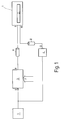
- the circuit shown in Figure 1 consists in its basic structure of a microprocessor 5, a parallel-serial converter 3 and a printhead 1.
- the latter is a thermal printhead for printing on a recording medium with a number of individually activatable heating elements which can be activated by means of a Register 2 can be controlled. Between the heating elements and a counter-pressure roller, the recording medium and - if the latter cannot be activated thermally - the effective run of an ink ribbon is arranged, so that a current flowing through the heating elements results in melting of particles of the ink ribbon and their transfer to the recording medium.
- the heating elements are activated during the printing process in accordance with the state stored by the individual elements of register 2.
- the register 2 is supplied with the data to be printed by a data line 11 through which the data are transmitted in serial form.
- the data are parallelized in the print head 1 by means of the register 2 in each case corresponding to a print line and are used for control the driver circuits of the heating elements.
- the microprocessor 5 transmits a print release signal to the print head 1, so that electrical current flows through the heating elements and a print series is printed on the recording medium .
- the data to be printed out is written into the parallel-serial converter 3 by data from the microprocessor 5 via a bus 7 (e.g. with 16 bits each).
- Clock signals of the microprocessor 5 are present at a clock input 6 of the converter 3. With each rising edge at the clock input 6, one bit is placed on an output 8 of the converter 3 and transmitted via the data line 11 to a data input 9 of the register 2.
- the clock signals of the microprocessor 5 are forwarded via a phase shifter 4, the function of which is described below, via a synchronization line 12 to a clock input 10 of the register 2.
- the state at the data input 9 is transferred to the first memory cell of the register 2 precisely when a rising edge is present at the clock input 10.
- Register 2 is thus a shift register. After a data word has been transferred to the register 2, the subsequent data words are successively written into the parallel-serial converter 3 via the bus 7 and transferred serially into the register 2 through the data line 11.
- the phase shifter 4 is provided, for example as an RC low-pass filter is feasible.
- a signal is present at its output 13, which is delayed in phase by approximately 90 ° with respect to the clock signal of the microprocessor 5.
- the phase shift thus corresponds to approximately a quarter of the clock time of the clock signal at the clock input 6 of the converter 3. Since a delayed signal is present at the clock input 10 of the register 2, the state of the data input 9 is only transferred to the register 2 after the by Vibrations caused by reflection have subsided. As a result, there is no longer any risk of data errors in register 2.
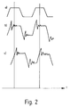
- Curve a) shows the curve shape at output 8 of parallel-serial converter 3. It is roughly rectangular with sloping flanks.
- the curve shown in b) corresponds to data input 9. Due to the mismatch of the input and output resistances of register 2 and converter 3 with the characteristic impedance of data line 11, superimposed oscillations occur on the rising and falling edges of the rectangular pulses, which decay exponentially. After a quarter of the cycle time, they have dropped to a negligible level.
- Curve c) represents the waveforms at clock input 10 of register 2. The square wave signals are also superimposed with vibrations at the reversal points. At the points in time identified by vertical lines in FIG.
- a D flip-flop 16 is used to improve the signal profiles at the data input 9.
- the state of the input 18 is around a clock signal delayed at output 19.
- the latter is connected to data input 9 of register 2 by data line 11.
- the input 18 of the flip-flop 16 is connected via a further line 20 to the output 8 of the parallel-serial converter 3.
- the clock output of the microprocessor 5 ′ is connected via a frequency bisector 14 to the clock input 6 of the parallel-serial converter 3 and the phase shifter 4, which in turn feeds the clock input 10.
- the clock frequency of the microprocessor 5 ' is therefore doubled compared to FIG. 1 with the same data transmission rate in line 11.
- phase shifter 15 is connected to the clock output of the microprocessor 5 ', the output of which feeds a clock input 17 of the flip-flop 16.
- the function of the parallel-serial converter 3, the phase shifter 4 and the register 2 correspond to the circuit shown in FIG. 1.
- the flip-flop 16 is arranged on the circuit board of the printer in the vicinity of the connection of the line 11 to the printhead; it serves to eliminate the reflections of the line 20, which is arranged between the parallel-serial converter 3 and the connection of the line 11. It would alternatively be conceivable to mount the flip-flop 16 on the print head 1, the line 11 being omitted.
- the flip-flop 16 initially takes over at a suitable time - determined by the phase shifter 15 - the state of its input 18 and transfers it to the register 2 at the second clock pulse.
- the phase shifter 15 can actually be an inverter.
- the data is then transferred into the flip-flop 16 after a quarter of a clock of the parallel-serial converter 3 has elapsed.
Landscapes
- Physics & Mathematics (AREA)
- Engineering & Computer Science (AREA)
- Mathematical Physics (AREA)
- General Engineering & Computer Science (AREA)
- General Physics & Mathematics (AREA)
- Theoretical Computer Science (AREA)
- Electronic Switches (AREA)
- Synchronisation In Digital Transmission Systems (AREA)
Applications Claiming Priority (2)
| Application Number | Priority Date | Filing Date | Title |
|---|---|---|---|
| DE1995121463 DE19521463A1 (de) | 1995-06-13 | 1995-06-13 | Schaltung zur Übertragung von Daten auf einen Druckkopf |
| DE19521463 | 1995-06-13 |
Publications (2)
| Publication Number | Publication Date |
|---|---|
| EP0749089A2 true EP0749089A2 (fr) | 1996-12-18 |
| EP0749089A3 EP0749089A3 (fr) | 1998-04-08 |
Family
ID=7764259
Family Applications (1)
| Application Number | Title | Priority Date | Filing Date |
|---|---|---|---|
| EP96102645A Withdrawn EP0749089A3 (fr) | 1995-06-13 | 1996-02-22 | Circuit pour transférer des données vers une tête d'impression |
Country Status (3)
| Country | Link |
|---|---|
| EP (1) | EP0749089A3 (fr) |
| JP (1) | JPH091848A (fr) |
| DE (1) | DE19521463A1 (fr) |
Cited By (1)
| Publication number | Priority date | Publication date | Assignee | Title |
|---|---|---|---|---|
| US7452041B2 (en) | 2003-08-07 | 2008-11-18 | Lexmark International, Inc. | Ink jet heater chip with internally generated clock signal |
Families Citing this family (2)
| Publication number | Priority date | Publication date | Assignee | Title |
|---|---|---|---|---|
| US6116767A (en) | 1997-04-30 | 2000-09-12 | Compaq Computer Corporation | Displaying audio disk track number in portable computer system |
| JP4750297B2 (ja) * | 2000-02-28 | 2011-08-17 | キヤノン株式会社 | 通信装置、方法、それを用いた画像形成装置、画像形成装置に接続されるユニット及び画像形成システム |
Family Cites Families (6)
| Publication number | Priority date | Publication date | Assignee | Title |
|---|---|---|---|---|
| JPH0775893B2 (ja) * | 1984-04-03 | 1995-08-16 | キヤノン株式会社 | プリンタ用の記録制御装置 |
| DE3732868A1 (de) * | 1987-09-25 | 1989-04-06 | Siemens Ag | Thermodruckverfahren und -vorrichtung |
| DE4016189A1 (de) * | 1990-05-19 | 1991-11-28 | Philips Patentverwaltung | Einrichtung zur phasenjitterreduzierung |
| DE4020719A1 (de) * | 1990-06-29 | 1992-01-02 | Broadcast Television Syst | Verfahren zur uebertragung eines digitalen datensignals |
| US5315320A (en) * | 1990-09-29 | 1994-05-24 | Kyocera Corporation | Mirror image printing printhead |
| EP0573936A1 (fr) * | 1992-06-08 | 1993-12-15 | Eastman Kodak Company | Modulateur puce à circuit intégré de tête d'impression avec circuit d'addresse de SRAM |
-
1995
- 1995-06-13 DE DE1995121463 patent/DE19521463A1/de not_active Withdrawn
-
1996
- 1996-02-22 EP EP96102645A patent/EP0749089A3/fr not_active Withdrawn
- 1996-04-26 JP JP10753496A patent/JPH091848A/ja active Pending
Cited By (1)
| Publication number | Priority date | Publication date | Assignee | Title |
|---|---|---|---|---|
| US7452041B2 (en) | 2003-08-07 | 2008-11-18 | Lexmark International, Inc. | Ink jet heater chip with internally generated clock signal |
Also Published As
| Publication number | Publication date |
|---|---|
| JPH091848A (ja) | 1997-01-07 |
| DE19521463A1 (de) | 1996-12-19 |
| EP0749089A3 (fr) | 1998-04-08 |
Similar Documents
| Publication | Publication Date | Title |
|---|---|---|
| EP0489944B1 (fr) | Procédé de communication de données maître-esclave avec bus flexible à un câble | |
| DE69031206T2 (de) | Rechnersystem | |
| DE19649258A1 (de) | Bussystem und Verfahren zur Datenübertragung | |
| DE3218741A1 (de) | Datentransfersystem | |
| DE69028498T2 (de) | Datenübertragungssystem und -verfahren | |
| DE68922984T2 (de) | Programmierbare Zeitsteuerung der Datenübertragung. | |
| DE69515018T2 (de) | Schaltung zur konversion serieller in parallele daten | |
| DE69403028T2 (de) | Verfahren und Vorrichtung zur Steuerung der Auf-dem-Chip-Taktverschiebung | |
| DE69801671T2 (de) | Verfahren und vorrichtung zur rückgewinnung von zeitverschobenen daten auf einem parallelen bus | |
| DE3042105C2 (fr) | ||
| DE69323789T2 (de) | Aufzeichnungsgerät | |
| DE3801993C2 (de) | Zeitgebersystem | |
| EP0749089A2 (fr) | Circuit pour transférer des données vers une tête d'impression | |
| DE69322941T2 (de) | Serieller Bus zwischen integrierten Schaltungen | |
| DE60015939T2 (de) | Verfahren und schaltung um an zwei enden getakten daten zu empfangen | |
| DE10241385A1 (de) | Integrierter Schaltkreis | |
| EP1148647A2 (fr) | Arrangement de circuit pour la réception d'au moins deux signaux digitaux | |
| EP0977406A1 (fr) | Circuit de transmission de signaux numériques avec séparation galvanique | |
| DE1774302B2 (de) | Verfahren und schaltungsanordnung zum ausgleich von zeitfehlern bei elektrischen signalen, die von einem informationstraeger abgenommen werden | |
| DE4413013C2 (de) | Video-Interfacesystem | |
| DE19724716A1 (de) | Synchrone serielle Datenübertragungseinrichtung | |
| DE69216178T2 (de) | Nahtlose Datenrückgewinnung | |
| DE19834190C2 (de) | Ausgabeverzögerungsschaltung | |
| DE3789943T2 (de) | Dateneingangsauswahl. | |
| DE102021124704A1 (de) | Vorrichtung zur Kompensation von Ausbreitungsverzögerungen, die bei einer Signalübertragung über Kabel auftreten |
Legal Events
| Date | Code | Title | Description |
|---|---|---|---|
| PUAI | Public reference made under article 153(3) epc to a published international application that has entered the european phase |
Free format text: ORIGINAL CODE: 0009012 |
|
| AK | Designated contracting states |
Kind code of ref document: A2 Designated state(s): DE ES FR |
|
| PUAL | Search report despatched |
Free format text: ORIGINAL CODE: 0009013 |
|
| RAP1 | Party data changed (applicant data changed or rights of an application transferred) |
Owner name: METO INTERNATIONAL GMBH |
|
| AK | Designated contracting states |
Kind code of ref document: A3 Designated state(s): DE ES FR |
|
| 17P | Request for examination filed |
Effective date: 19980305 |
|
| STAA | Information on the status of an ep patent application or granted ep patent |
Free format text: STATUS: THE APPLICATION HAS BEEN WITHDRAWN |
|
| 18W | Application withdrawn |
Withdrawal date: 19990415 |