EP0756401A2 - Vorrichtung zur seriellen Übertragung von asynchronen Daten mit Flanken- und Zeitgeberunterbrechnungsarbeitsweise - Google Patents
Vorrichtung zur seriellen Übertragung von asynchronen Daten mit Flanken- und Zeitgeberunterbrechnungsarbeitsweise Download PDFInfo
- Publication number
- EP0756401A2 EP0756401A2 EP96112152A EP96112152A EP0756401A2 EP 0756401 A2 EP0756401 A2 EP 0756401A2 EP 96112152 A EP96112152 A EP 96112152A EP 96112152 A EP96112152 A EP 96112152A EP 0756401 A2 EP0756401 A2 EP 0756401A2
- Authority
- EP
- European Patent Office
- Prior art keywords
- timer
- data transmission
- bit
- add
- edge
- Prior art date
- Legal status (The legal status is an assumption and is not a legal conclusion. Google has not performed a legal analysis and makes no representation as to the accuracy of the status listed.)
- Granted
Links
Images










Classifications
-
- H—ELECTRICITY
- H04—ELECTRIC COMMUNICATION TECHNIQUE
- H04L—TRANSMISSION OF DIGITAL INFORMATION, e.g. TELEGRAPHIC COMMUNICATION
- H04L25/00—Baseband systems
- H04L25/38—Synchronous or start-stop systems, e.g. for Baudot code
- H04L25/40—Transmitting circuits; Receiving circuits
- H04L25/45—Transmitting circuits; Receiving circuits using electronic distributors
-
- H—ELECTRICITY
- H04—ELECTRIC COMMUNICATION TECHNIQUE
- H04L—TRANSMISSION OF DIGITAL INFORMATION, e.g. TELEGRAPHIC COMMUNICATION
- H04L12/00—Data switching networks
- H04L12/28—Data switching networks characterised by path configuration, e.g. LAN [Local Area Networks] or WAN [Wide Area Networks]
- H04L12/40—Bus networks
-
- H—ELECTRICITY
- H04—ELECTRIC COMMUNICATION TECHNIQUE
- H04L—TRANSMISSION OF DIGITAL INFORMATION, e.g. TELEGRAPHIC COMMUNICATION
- H04L12/00—Data switching networks
- H04L12/28—Data switching networks characterised by path configuration, e.g. LAN [Local Area Networks] or WAN [Wide Area Networks]
- H04L12/40—Bus networks
- H04L12/407—Bus networks with decentralised control
- H04L12/413—Bus networks with decentralised control with random access, e.g. carrier-sense multiple-access with collision detection [CSMA-CD]
- H04L12/4135—Bus networks with decentralised control with random access, e.g. carrier-sense multiple-access with collision detection [CSMA-CD] using bit-wise arbitration
-
- H—ELECTRICITY
- H04—ELECTRIC COMMUNICATION TECHNIQUE
- H04L—TRANSMISSION OF DIGITAL INFORMATION, e.g. TELEGRAPHIC COMMUNICATION
- H04L49/00—Packet switching elements
- H04L49/90—Buffering arrangements
-
- H—ELECTRICITY
- H04—ELECTRIC COMMUNICATION TECHNIQUE
- H04L—TRANSMISSION OF DIGITAL INFORMATION, e.g. TELEGRAPHIC COMMUNICATION
- H04L5/00—Arrangements affording multiple use of the transmission path
- H04L5/14—Two-way operation using the same type of signal, i.e. duplex
- H04L5/16—Half-duplex systems; Simplex/duplex switching; Transmission of break signals non-automatically inverting the direction of transmission
-
- H—ELECTRICITY
- H04—ELECTRIC COMMUNICATION TECHNIQUE
- H04L—TRANSMISSION OF DIGITAL INFORMATION, e.g. TELEGRAPHIC COMMUNICATION
- H04L12/00—Data switching networks
- H04L12/28—Data switching networks characterised by path configuration, e.g. LAN [Local Area Networks] or WAN [Wide Area Networks]
- H04L12/40—Bus networks
- H04L12/407—Bus networks with decentralised control
-
- H—ELECTRICITY
- H04—ELECTRIC COMMUNICATION TECHNIQUE
- H04L—TRANSMISSION OF DIGITAL INFORMATION, e.g. TELEGRAPHIC COMMUNICATION
- H04L12/00—Data switching networks
- H04L12/28—Data switching networks characterised by path configuration, e.g. LAN [Local Area Networks] or WAN [Wide Area Networks]
- H04L12/40—Bus networks
- H04L2012/4026—Bus for use in automation systems
-
- H—ELECTRICITY
- H04—ELECTRIC COMMUNICATION TECHNIQUE
- H04L—TRANSMISSION OF DIGITAL INFORMATION, e.g. TELEGRAPHIC COMMUNICATION
- H04L7/00—Arrangements for synchronising receiver with transmitter
- H04L7/02—Speed or phase control by the received code signals, the signals containing no special synchronisation information
- H04L7/033—Speed or phase control by the received code signals, the signals containing no special synchronisation information using the transitions of the received signal to control the phase of the synchronising-signal-generating means, e.g. using a phase-locked loop
- H04L7/0331—Speed or phase control by the received code signals, the signals containing no special synchronisation information using the transitions of the received signal to control the phase of the synchronising-signal-generating means, e.g. using a phase-locked loop with a digital phase-locked loop [PLL] processing binary samples, e.g. add/subtract logic for correction of receiver clock
-
- H—ELECTRICITY
- H04—ELECTRIC COMMUNICATION TECHNIQUE
- H04L—TRANSMISSION OF DIGITAL INFORMATION, e.g. TELEGRAPHIC COMMUNICATION
- H04L7/00—Arrangements for synchronising receiver with transmitter
- H04L7/04—Speed or phase control by synchronisation signals
- H04L7/041—Speed or phase control by synchronisation signals using special codes as synchronising signal
- H04L7/044—Speed or phase control by synchronisation signals using special codes as synchronising signal using a single bit, e.g. start stop bit
-
- H—ELECTRICITY
- H04—ELECTRIC COMMUNICATION TECHNIQUE
- H04L—TRANSMISSION OF DIGITAL INFORMATION, e.g. TELEGRAPHIC COMMUNICATION
- H04L7/00—Arrangements for synchronising receiver with transmitter
- H04L7/04—Speed or phase control by synchronisation signals
- H04L7/08—Speed or phase control by synchronisation signals the synchronisation signals recurring cyclically
Definitions
- the present invention relates to an asynchronous serial data transmission apparatus.
- transmission parameters such as a transmission baud rate, a length of data bits, a form of parity, a length of stop bits of a master unit, i.e., a transmitting side must be completely consistent with those of a slave unit, i.e., a receiving side.
- a master unit i.e., a transmitting side
- a slave unit i.e., a receiving side.
- the date formats are relatively simple, and therefore, it is easy to make one of the data formats conform to the other.
- an edge detector detects an edge in a signal at the data transmission bus.
- An edge interrupt operation is carried out to operate a timer in response to the edge.
- the edge interrupt operation is stopped when the timer is being operated.
- a timer interrupt operation carries out a fetching operation of a bit data on the data transmission bus in a receiving mode or a transmitting operation of a bit data to the data transmission bus in a transmitting mode, in response to the timer means whose content reaches a predetermined value.
- Fig. 1 which shows a signal format of a prior art start-stop transmission system which is a typical asynchronous transmission system
- one frame is comprised of a start bit ST, 5 to 8 data bits D, a parity bit P, and one or two stop bits SP.
- the start bit ST shows a start of transmission, and has a pulse of "0" having a length of one bit. Note that a level immediately before the start pulse ST is "1".
- the data bits D show a content of transmitting data.
- the parity bit P shows a checking bit of the data bits D. That is, the parity bit P shows an addition result of each of the data bits D (mod 2).
- the stop bits SP show an end of transmission as well as an advance notice of the next start of transmission, and have a pulse of "1".
- a time period T for one bit is constant.
- transmission parameters such as a transmission baud rate, a length of data bits, a form of the parity, a length of stop bits of a master unit, i.e., a transmitting side must be completely consistent with those of a slave unit, i.e., a receiving side.
- a master unit i.e., a transmitting side
- a slave unit i.e., a receiving side.
- the data formats are relatively simple, and therefore, it is easy to make one of the data formats conform to the other.
- D2B digital bus
- IEC International Electrotechnical Committee
- one frame of a D2B protocol is comprised of a header 101, a master address field 102, a slave address field 103, a control field 104 and a data field 105.
- the header 101 includes a start bit ST showing a start of transmission and a mode bit M showing a transmission baud rate.
- the master address field 102 includes master address bits showing an address of a master unit and a parity bit P.
- the slave address field 103 includes slave address bits showing an address of a slave unit, a parity bit P, and an acknowledgement bit A.
- the control field 104 includes control bits showing a content of transmission from the master unit to the slave unit and vice versa and transmission of a command from the master unit to the slave unit, a parity bit P and an acknowledgement bit A.
- the data field 105 includes a series of 8-bit data (or commands), each of which is followed by an end-of-data E, a parity bit P and an acknowledgement bit A. Note that, if the end-of-data E is "0", the data is ended, while if the end-of-data E is "1", the data is continued.
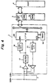
- a serial data transmission apparatus 1 is connected between a D2B bus 2 formed by lines D2B+ and D2B- and a host interface 3.
- the host interface 3 is connected to a host controller 4.
- the serial data transmission apparatus 1 includes a D2B receiver 11 for receiving data from the D2B bus 2 and a D2B transmitter 12 for tranmitting data to the D2B bus 2.
- a shift register 13 stores data from the D2B receiver 11.
- An arbitration detector 14 performs an occupying operation upon the D2B bus 2.
- a parity checking circuit 15 performs a parity checking operation upon each field.
- the shift register 13, the arbitration detector 14 and the parity checking circuit 15 are connected to a protocol controller 16 which controls serial data transmission.
- the host interface 3 includes a read data buffer 31 for storing data from the serial data transmission apparatus 1 in a receiving mode, Also, the host interface 3 includes a write data buffer 32 for storing data to be transmitted to the serial data transmission apparatus 1 in a transmitting mode.
- a receiving operation of the serial data transmission apparatus 1 of Fig. 3 is carried out as follows. That is, data from the D2B receiver 11 is written into the shift register 13. When an amount of data written into the shift register 13 reaches a predetermined amount, the data of the shift register 13 are transferred in parallel to the protocol controller 16. Simultaneously, a parity chewing operation is performed by the parity checking circuit 15 upon the data from the D2B receiver 11, and the result of parity checking is transferred to the protocol controller 16. Then, if the parity checking result is successful, the protocol controller 16 transmits received data to the read data buffer 31 of the host interface 3.
- a transmitting operation of the serial data transmission apparatus 1 of Fig. 2 is carried out as follows. That is, when the protocol controller 16 receives data to be transmitted from the write data buffer 2032 of the host interface 3, the arbitration detector 14 performs an occupying operation upon the D2B bus 2, and after the D2B bus 2 is occupied by the serial data transmission apparatus 1, the protocol controller 16 transmits the data via the D2B driver 12 to the D2B bus 2.
- serial data transmission apparatus 1 of Fig. 3 Since the serial data transmission apparatus 1 of Fig. 3 is required to respond to an accurate synchronization, a bus occupying operation in a transmitting operation and a high speed operation, the serial data transmission apparatus 1 has become more complex and more expensive.
- a serial data transmission apparatus 1' includes a filter 17, an edge detector 18, a timer 19, a central processing unit (CPU) 20 and a serial interface 21 instead of the shift register 13, the arbitration detector 14, the parity check circuit 15 and the protocol controller 16 of Fig. 3. That is, when an output signal of the edge detector 18 is input to an interrupt terminal INT1 of the CPU 20, an edge detection interrupt routine, which will be explained later, is carried out. Also, when an output signal of the timer 19 is input to an interrupt terminal INT2 of the CPU 20, a timer interrupt routine, which will be explained later, is carried out.
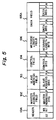
- a header 101A includes a multiaddress bit instead of the mode bit M of the header 101 of Fig. 2, and a data field 105A does not include the end-of-data E of the data field 105 of Fig. 2.
- a message length field 106 is added to define the number of bytes of the data field 105A.
- the message length field 106 includes message length bits followed by a parity bit P and an acknowledgement bit A.
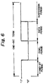
- a term of each bit is comprised of a stand-by time period having a value "1", a synchronization time period having a value "0", a data time period having a value depending upon the value of the bit, and a suspension time period having a value "1".
- a length of the synchronization time period is approximately the same as a length of the data time period.
- the edge detection interrupt routine is shown in Fig. 7.
- step 701 it is determined whether or not an edge detection interrupt operation is allowed. Note that, when a timer interrupt operation is being carried out, the edge detection interrupt operation is prohibited. Only if the edge detection interrupt operation is allowed, does the control proceed to step 702. Otherwise, the control proceeds directly to step 706.
- step 702 a sampling time to be set in the timer 19 is calculated.
- step 703 the sampling time is set in the timer 19, and the timer 19 is started.
- step 704 the edge detection interrupt operation is prohibited, while, at step 705, the timer interrupt operation is allowed.
- step 706 The edge detection interrupt routine of Fig. 7 is completed by step 706.
- the timer interrupt routine is shown in Fig. 8.
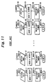
- step 801 it is determined whether or not a timer interrupt operation is allowed. Note that the timer interrupt operation is allowed by step 705 of Fig. 7. If the timer interrupt operation is prohibited, the control proceeds to step 802. If the timer interrupt operation is allowed, the control proceeds to step 803.
- an address ADD is determined. Note that the address ADD is initialized at ADD1 for a receiving mode, and the address ADD is initialized at ADD1' for a transmitting mode.
- ADD is equal to ADD1
- a receiving process of a start bit ST is carried out at step 804.
- ADD is equal to ADD2
- a receiving process of a multiaddress bit is carried out at step 805.
- ADD is equal to ADD3, ADD4, ⁇ , or ADD15
- a receiving process of a master address field is carried out at step 807.
- ADD is equal to ADD16, ADD17, ⁇ , or ADD29
- a receiving process of a slave address field is carried out at step 809.
- ADD is equal to ADD30, ADD31, ⁇ , or ADD35
- a receiving process of a control field is carried out at step 811.
- ADD is equal to ADD36, ADD37, ⁇ , or ADD45
- a receiving process of a message length field is carried out at step 813.
- ADD is equal to ADD46, ADD47, ⁇ , or ADD55
- a receiving process of a data field is carried out at step 815.
- ADD is equal to ADD2', ADD3', ⁇ , or ADD14'
- a transmitting process of a master address field is carried out at step 808.
- ADD is equal to ADD15', ADD16', ⁇ , or ADD28'
- a transmitting process of a slave address field is carried out at step 810.
- ADD is equal to ADD35', ADD36', ⁇ , or ADD44'
- a transmitting process of a message length field is carried out at step 814.
- ADD is equal to ADD45', ADD46', or the like a transmitting process of a data field is carried out at step 816.
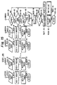
- Fig. 9 which is a detailed flowchart of step 804 of Fig. 8, at step 901, a start pulse ST is fetched from the filter 17 of Fig. 4. Next, at step 902, the address ADD is caused to be ADD2. Next, at step 903, the sampling time is set in the timer 19 and the timer 19 is restarted. Then, the routine of Fig. 8 is completed by step 904.
- Fig. 10 which is a detailed flowchart of step 805 of Fig. 8, at step 1001, a multiaddress (MA) bit is fetched from the filter 17 of Fig. 4. Next, at step 1002, the address ADD is caused to be ADD3. Next, at step 1003, the sampling time is set in the timer 19 and the timer 19 is restarted. Then, the routine of Fig. 8 is completed by step 1004.
- MA multiaddress
- MSB most significant bit
- step 1001-2 a master address bit M10, is fetched from the filter 17 of Fig. 4.
- step 1002-2 the address ADD is caused to be ADD5.
- step 1003-2 the sampling time is set in the timer 19 and the timer 19 is restarted. Then, the routine of Fig. 8 is completed by step 1004-2.
- step 1001-12 a least significant bit (LSB) M00 of the master address bits is fetched from the filter 17 of Fig. 4.
- step 1002-12 the address ADD is caused to be ADD15.
- step 1003-12 the sampling time is set in the timer 19 and the timer 19 is restarted. Then, the routine of Fig. 8 is completed by step 1004-12.
- step 1001-13 a parity bit P of the master address bits is fetched from the filter 17 of Fig. 4.
- step 1002-13 the address ADD is caused to be ADD16.
- step 1003-13 the sampling time is set in the timer 19 and the timer 19 is restarted. Then, the routine of Fig. 8 is completed by step 1004-13.
- step 1201-2 a slave address bit S10 is fetched from the filter 17 of Fig. 4.
- step 1202-2 the address ADD is caused to be ADD18.
- step 1203-2 the sampling time is set in the timer 19 and the timer 19 is restarted. Then, the routine of Fig. 8 is completed by step 1204-2.
- step 1201-12 an LSB S00 of the slave address bits is fetched from the filter 17 of Fig. 4.
- the address ADD is caused to be ADD28.
- step 1203-12 the sampling time is set in the timer 19 and the timer 19 is restarted. Then, the routine of Fig. 8 is completed by step 1204-12.
- step 1201-13 a parity bit P of the slave address bits is fetched from the filter 17 of Fig. 4.
- step 1202-13 the address ADD is caused to be ADD29.
- step 1203-13 the sampling time is set in the timer 19 and the timer 19 is restarted. Then, the routine of Fig. 8 is completed by step 1204-13.
- step 1201-14 it is determined whether or not the received master address bits M11 to M00 and the received slave address bits S11 to S00 are correct in accordance with their received parities P. Also, it is determined whether or not the received slave bits S11 to S00 indicate the address of this slave unit. As a result, only when the received master address bits and the received slave address bits are correct and the received slave address bits indicate the address of this slave unit, does the control proceed to step 1202-14. Otherwise, the control proceeds to step 1206-14. At step 1202-14, it is determined whether or not the received multiaddress (MA) bit is "0" (active). Only when the multiaddress bit is "1", does the control proceed to step 1203-14.
- MA multiaddress
- step 1204-14 an acknowledgement bit A is transmitted via the serial interface 21 and the D2B transmitter 12 to the master unit.
- the address ADD is caused to be ADD30.
- the sampling time is set in the timer 19 and the timer 19 is restarted.
- the address ADD is caused to be ADD1
- the edge detection interrupt operation is allowed and the timer interrupt operation is prohibited, thus initializing the receiving mode.
- the routine of Fig. 8 is completed by step 1208-14.
- step 1301-2 a control bit C02 is fetched from the filter 17 of Fig. 4.
- step 1302-2 the address ADD is caused to be ADD32.
- step 1303-2 the sampling time is set in the timer 19 and the timer 19 is restarted. Then, the routine of Fig. 8 is completed by step 1304-2.
- step 1301-4 an LSB C00 of the control bits is fetched from the filter 17 of Fig. 4.
- step 1302-4 the address ADD is caused to be ADD34.
- step 1303-4 the sampling time is set in the timer 19 and the timer 19 is restarted. Then, the routine of Fig. 8 is completed by step 1304-4.
- step 1301-5 a parity bit P of the control bits is fetched from the filter 17 Fig. 4.
- step 1302-5 the address ADD is caused to be ADD35.
- step 1303-5 the sampling time is set in the timer 19 and the timer 19 is restarted. Then, the routine of Fig. 8 is completed by step 1304-5.
- step 1301-6 it is determined whether or not the received control bits C03 to C00 are correct in accordance with their received parity P. As a result, only when the received control bits are correct, does the control proceed to step 1302-6. Otherwise, the control proceeds to step 1306-6.
- step 1302-6 it is determined whether or not the received multiaddress (MA) bit is "0" (active). Only when the multiaddress bit is "1”, does the control proceed to step 1303-6. Otherwise, the control proceeds directly to step 1304-6.
- an acknowledgement bit A is transmitted via the serial interface 21 and the D2B transmitter 12 to the master unit.
- the address ADD is caused to be ADD36.
- step 1305-6 the sampling time is set in the timer 19 and the timer 19 is restarted.
- step 1306-6 the address ADD is caused to be ADD1, and at step 1307-6, the edge detection interrupt operation is allowed and the timer interrupt operation is prohibited, thus initializing the receiving mode. Then, the routine of Fig. 8 is completed by step 1308-6.
- step 1402-1 a message length bit L06 is fetched from the filter 17 of Fig. 4.
- step 1402-2 the address ADD is caused to be ADD38.
- step 1403-2 the sampling time is set in the timer 19 and the timer 19 is restarted. Then, the routine of Fig. 8 is completed by step 1404-2.
- step 1401-8 an LSB L00 of the message length bits, is fetched from the filter 17 of Fig. 4.
- the address ADD is caused to be ADD44.
- step 1403-8 the sampling time is set in the timer 19 and the timer 19 is restarted. Then, the routine of Fig. 8 is completed by step 1404-8.
- step 1401-9 a parity bit P of the message length bits is fetched from the filter 17 Fig. 4.
- step 1402-9 the address ADD is caused to be ADD45.
- step 1403-9 the sampling time is set in the timer 19 and the timer 19 is restarted. Then, the routine of Fig. 8 is completed by step 1404-9.
- step 1401-10 it is determined whether or not the received message length bits L07 to L00 are correct in accordance with its received parity P. As a result, only when the received message length bits are correct, does the control proceed to step 1402-10. Otherwise, the control proceeds to step 1406-10.
- step 1402-10 it is determined whether or not the received multiaddress (MA) bit is "0" (active). Only when the multiaddress bit is "1”, does the control proceed to step 1403-10. Otherwise, the control proceeds directly to step 1404-10.
- an acknowledgement bit A is transmitted via the serial interface 21 and the D2B transmitter 12 to the master unit.
- step 1404-10 the address ADD is caused to be ADD46. Then, at step 1405-10, the sampling time is set in the timer 19 and the timer 19 is restarted. On the other hand, at step 1406-10, the address ADD is caused to be ADD1, and at step 1407-10, the edge detection interrupt operation is allowed and the timer interrupt operation is prohibited, thus initializing the receiving mode. Then, the routine of Fig. 8 is completed by step 1408-10.
- message length bits (M07, M06, ⁇ , M00) define the number of bytes of data in the data field as follows:
- step 1501-2 a second bit D06 of the one-byte data is fetched from the filter 17 of Fig. 4.
- the address ADD is caused to be ADD48.
- step 1503-2 the sampling time is set in the timer 19 and the timer 19 is restarted. Then, the routine of Fig. 8 is completed by step 1504-2.
- step 1501-8 an LSB D00 of the one-byte data is fetched from the filter 17 of Fig. 4.
- the address ADD is caused to be ADD54.
- step 1503-12 the sampling time is set in the timer 19 and the timer 19 is restarted. Then, the routine of Fig. 8 is completed by step 1504-8.
- step 1501-9 a parity bit P of the one-byte data is fetched from the filter 17 of Fig. 4.
- the address ADD is caused to be ADD55.
- step 1503-9 the sampling time is set in the timer 19 and the timer 19 is restarted. Then, the routine of Fig. 8 is completed by step 1504-9.
- step 1501-10 it is determined whether or not the received one-byte data bits D07 to D00 are correct in accordance with its received parity P. As a result, only when the received data bits are correct, does the control proceed to step 1502-10. Otherwise, the control proceeds to step 1509-10.
- step 1502-10 it is determined whether or not the read data buffer 31 of Fig. 4 is empty. Only when the read data buffer 31 is empty, does the control proceed to step 1503-10. Otherwise, the control proceeds to step 1509-10.
- step 1503-10 it is determined whether or not the received multiaddress (MA) bit is "0" (active). Only when the multiaddress bit is "1", does the control proceed to step 1504-10.
- MA received multiaddress
- step 1505-10 an acknowledgement bit A is transmitted via the serial interface 21 and the D2B transmitter 12 to the master unit.
- the received number L of bytes is counted down by 1, i.e., L ⁇ L-1
- step 1505-11 it is determined whether or not the number L has reached 0. Only when L reaches 0, does the control proceed to step 1509-10. Otherwise, the control proceeds to step 1507-10.
- the address ADD is caused to be ADD30.
- step 1508-10 the sampling time is set in the timer 19 and the timer 19 is restarted.
- step 1509-10 the address ADD is caused to be ADD1, and at step 1510-10, the edge detection interrupt operation is allowed and the timer interrupt operation is prohibited, thus initializing the receiving mode. Then, the routine of Fig. 8 is completed by step 1511-11.
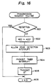
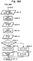
- Fig. 16 which is a transmission request routine, this routine is carried out when data to be transmitted is written into the write data buffer 32 of Fig. 4.
- step 1601 it is determined whether or not the serial data transmission apparatus 1' is currently in a receiving mode. Note that, if the serial data transmission apparatus 1' of Fig. 4 is in a receiving mode, the address ADD is ADD2, ADD3, ⁇ , or ADD55. Therefore, at step 1601, it is determined whether or not the address ADD is one of ADD2, ADD3, ⁇ , and ADD55. Unless the address ADD is one of ADD2, ADD3, ⁇ , and ADD55, the control proceeds to steps 1602, 1603 and 1604. If the address ADD is one of ADD2, ADD3, ⁇ , and ADD55, the control proceeds directly to step 1606.
- ADD1' is set in the address ADD.
- the edge detection interrupt operation is allowed, while, at step 1604, the timer interrupt operation is prohibited.
- a start pulse ST is transmitted to the D2B bus 2.
- step 1606 the routine of Fig. 16 is completed by step 1606.
- the edge detection interrupt routine shown in Fig. 7 is carried out. That is, the control proceeds via step 701 to step 702. At step 702, a sampling time to be set in the timer 19 is calculated. Then, at step 703, the sampling time is set in the timer 19, and the timer 19 is started. Next, at step 704, the edge detection interrupt operation is prohibited, while, at step 705, the timer interrupt operation is allowed. The edge detection interrupt routine of Fig. 7 is completed by step 706.
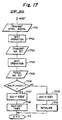
- a synchronization signal is transmitted to the D2B bus 2, and at step 1702, a wait operation is carried out to maintain the synchronization signal for a synchronization period (see Fig. 6).
- a multiaddress bit signal MA(T) is transmitted to the D2B bus 2
- a wait operation is carried out to maintain the multiaddress bit signal for a wait period TD.
- a signal MA(R) is fetched from the filter 17 of Fig. 4.
- step 1707 the address ADD is caused to be ADD2'. Then, at step 1708, the sampling time is set in the timer 19 and the timer 19 is restarted.
- step 1709 the address ADD is caused to be ADD1
- step 1710 the edge detection interrupt operation is allowed and the timer interrupt operation is prohibited, thus changing the transmitting mode into a standby state for a receiving mode.
- step 1711 The routine of Fig. 8 is completed by step 1711.
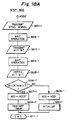
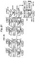
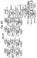
- Figs. 18A, 18B, 18C and 18D are detailed flowcharts of step 808 of Fig. 8.
- a synchronization signal is transmitted to the D2B bus 2, and at step 1802-1, a wait operation is carried out to maintain the synchronization signal for a synchronization period (see Fig. 6).
- an MSB M11 of master address bits is transmitted to the D2B bus 2
- a wait operation is carried out to maintain the MSB M11 for a wait period TD.
- a signal M11(R) is fetched from the filter 17 of Fig. 4.
- step 1807-1 the address ADD is caused to be ADD3'. Then, at step 1808-1, the sampling time is set in the timer 19 and the timer 19 is restarted.
- step 1809-1 the address ADD is caused to be ADD1
- step 1810-1 the edge detection interrupt operation is allowed and the timer interrupt operation is prohibited, thus changing the transmitting mode into a standby state for a receiving mode.
- a synchronization signal is transmit-to to the D2B bus 2, and at step 1802-2, a wait operation is carried out to maintain the synchronization signal for a synchronization period (see Fig. 6).
- a master address bit M10 is transmitted to the D2B bus 2, and at step 1804-2, a wait operation is carried out to maintain the master address bit M10 for a wait period TD.
- a signal M10(R) is fetched from the filter 17 of Fig. 4.
- step 1807-2 the address ADD is caused to be ADD4'. Then, at step 1808-2, the sampling time is set in the timer 19 and the timer 19 is restarted.
- step 1809-2 the address ADD is caused to be ADD1
- step 1810-2 the edge detection interrupt operation is allowed and the timer interrupt operation is prohibited, thus changing the transmitting mode into a standby state for a receiving mode.
- a synchronization signal is transmitted to the D2B bus 2, and at step 1802-12, a wait operation is carried out to maintain the synchronization signal for a synchronization period (see Fig. 6).
- an LSB M00 of the master address bits is transmitted to the D2B bus 2, and at step 1804-12, a wait operation is carried out to maintain the LSB M00 for a wait period TD.
- a signal M00(R) is fetched from the filter 17 of Fig. 4.
- step 1807-12 the address ADD is caused to be ADD14'. Then, at step 1808-12, the sampling time is set in the timer 19 and the timer 19 is restarted.
- step 1809-12 the address ADD is caused to be ADD1
- step 1810-12 the edge detection interrupt operation is allowed and the timer interrupt operation is prohibited, thus changing the transmitting mode into a standby state for a receiving mode.
- a synchronization signal is transmitted to the D2B bus 2, and at step 1802-13, a wait operation is carried out to maintain the synchronization signal for a synchronization period (see Fig. 6).
- a parity bit P of the master address bits is transmitted to the D2B bus 2, and at step 1804-12, a wait operation is carried out to maintain the parity bit P for a wait period TD.
- a signal P(R) is fetched from the filter 17 of Fig. 4.
- step 1807-13 the address ADD is caused to be ADD15'. Then, at step 1808-13, the sampling time is set in the timer 19 and the timer 19 is restarted.
- step 1809-13 the address ADD is caused to be ADD1, and at step 1810-13, the edge detection interrupt operation is allowed and the timer interrupt operation is prohibited, thus changing the transmitting mode into a standby state for a receiving mode.
- TD 2ab/(1 - a) + (1 + a)(1T d + 2T t + T r ) + T r
- step 1902-1 the address ADD is caused to be ADD16'.
- step 1903-1 the sampling time is set in the timer 19 and the timer 19 is restarted. Then, the routine of Fig. 8 is completed by step 1904-1.
- step 1901-2 a slave address bit S10 is transmitted via the serial interface 21 and the D2B transmitter 12 to the D2B bus 2.
- step 1902-2 the address ADD is caused to be ADD17'.
- step 1903-2 the sampling time is set in the timer 19 and the timer 19 is restarted. Then, the routine of Fig. 8 is completed by step 1904-2.
- step 1901-12 an LSB S00 of the slave address bits is transmitted via the serial interface 21 and the D2B transmitter 12 to the D2B bus 2.
- step 1902-12 the address ADD is caused to be ADD27'.
- step 1903-12 the sampling time is set in the timer 19 and the timer 19 is restarted. Then, the routine of Fig. 8 is completed by step 1904-12.
- step 1901-13 a parity bit P of the slave address bits is transmitted via the serial interface 21 and the D2B transmitter 12 to the D2B bus 2.
- step 1902-13 the address ADD is caused to be ADD28'.
- step 1903-13 the sampling time is set in the timer 19 and the timer 19 is restarted. Then, the routine of Fig. 8 is completed by step 1904-13.
- step 1901-14 it is determined whether or not the transmitted multiaddress (MA) bit is "0" (active). Only when the multiaddress bit is "1", does the control proceed to step 1902-14. Otherwise, the control proceeds directly to step 1902-14.
- the acknowledgement bit A from the slave unit is fetched, and at step 1903-14, it is determined whether or not the acknowledgement bit is "0" (active). Only when the acknowledgement bit A is "0”, does the control proceed to steps 1904-14 and 1905-14. Otherwise, the control proceeds to steps 1906-14 and 1907-14.
- step 1904-14 the address ADD is caused to be ADD29'.
- step 1905-14 the sampling time is set in the timer 19 and the timer 19 is restarted.
- step 1906-14 the address ADD is caused to be ADD1
- step 1907-14 the edge detection interrupt operation is allowed and the timer interrupt operation is prohibited, thus changing the transmitting mode into a standby state for a receiving mode.
- the routine of Fig. 8 is completed by step 1908-14.
- step 2002-1 the address ADD is caused to be ADD30'.
- step 2003-1 the sampling time is set in the timer 19 and the timer 19 is restarted. Then, the routine of Fig. 8 is completed by step 2004-1.
- step 2001-2 a control bit C02 is transmitted via the serial interface 21 and the D2B transmitter 12 to the D2B bus 2.
- step 2002-2 the address ADD is caused to be ADD31'.
- step 2003-2 the sampling time is set in the timer 19 and the timer 19 is restarted. Then, the routine of Fig. 8 is completed by step 2004-2.
- step 2001-4 an LSB C00 of the control bits, is transmitted via the serial interface 21 and the D2B transmitter 12 to the D2B bus 2.
- step 2002-4 the address ADD is caused to be ADD33'.
- step 2003-4 the sampling time is set in the timer 19 and the timer 19 is restarted. Then, the routine of Fig. 8 is completed by step 2004-4.
- step 2001-5 a parity bit P of the control bits is transmitted via the serial interface 21 and the D2B transmitter 12 to the D2B bus 2.
- step 2002-5 the address ADD is caused to be ADD34'.
- step 2003-4 the sampling time is set in the timer 19 and the timer 19 is restarted. Then, the routine of Fig. 8 is completed by step 2004-4.
- step 2001-6 it is determined whether or not the transmitted multiaddress (MA) bit is "0" (active). Only when the multiaddress bit is "1", does the control proceed to step 2002-6. Otherwise, the control proceeds directly to step 2002-6.
- step 2002-6 the acknowledgement bit A from the slave unit is fetched, and at step 2003-6, it is determined whether or not the acknowledgement bit A is "0" (active). Only when the acknowledgement bit A is "0”, does the control proceed to steps 2004-6 and 2004-6. Otherwise, the control proceeds to steps 2006-6 and 2007-6.
- step 2004-6 thd address ADD is caused to be ADD35'.
- step 2005-6 the sampling time is set in the timer 19 and the timer 19 is restarted.
- step 2006-6 the address ADD is caused to be ADD1
- step 2007-6 the edge detection interrupt operation is allowed and the timer interrupt operation is prohibited, thus changing the transmitting mode into a standby state for a receiving mode.
- the routine of Fig. 8 is completed by step 2008-6.
- step 2102-1 the address ADD is caused to be ADD37'.
- step 2103-1 the sampling time is set in the timer 19 and the timer 19 is restarted. Then, the routine of Fig. 8 is completed by step 2104-1.
- a message length bit L06 is transmitted via the serial interface 21 and the D2B transmitter 12 to the D2B bus 2.
- the address ADD is caused to be ADD28'.
- the sampling time is set in the timer 19 and the timer 19 is restarted. Then, the routine of Fig. 8 is completed by step 2104-2.
- step 2101-8 an LSB S00 of the slave address bits is transmitted via the serial interface 21 and the D2B transmitter 12 to the D2B bus 2.
- step 2102-8 the address ADD is caused to be ADD43'.
- step 2103-8 the sampling time is set in the timer 19 and the timer 19 is restarted. Then, the routine of Fig. 8 is completed by step 2104-8.
- step 2101-9 a parity bit P of the slave address bits, is transmitted via the serial interface 21 and the D2B transmitter 12 to the D2B bus 2.
- step 2102-9 the address ADD is caused to be ADD44'.
- step 2103-9 the sampling time is set in the timer 19 and the timer 19 is restarted. Then, the routine of Fig. 8 is completed by step 2104-9.
- step 2101-10 it is determined whether or not the transmitted multiaddress (MA) bit is "0" (active). Only when the multiaddress bit is "1", does the control proceed to step 2102-10. Otherwise, the control proceeds directly to step 2102-10.
- the acknowledgement bit A from the slave unit is fetched, and at steps 2103-10, it is determined whether or riot the acknowledgement bit is "0" (active). Only when the acknowledgement bit A is "0”, does the control proceed to steps 2104-10 and 2104-10. Otherwise, the control proceeds to steps 2106-10 and 2107-10.
- the address ADD is caused to be ADD45'.
- step 2105-10 the sampling time is set in the timer 19 and the timer 19 is restarted.
- step 2106-10 the address ADD is caused to be ADD1, and at step 2107-10, the edge detection interrupt operation is allowed and the timer interrupt operation is prohibited, thus changing the transmitting mode into a standby state for a receiving mode.
- the routine of Fig. 8 is completed by step 2108-10.
- step 2201-2 a second bit D06 of the one-byte data is transmitted via the serial interface 21 and the D2B transmitter 12 to the D2B bus 2.
- step 2202-2 the address ADD is caused to be ADD47'.
- step 2203-2 the sampling time is set in the timer 19 and the timer 19 is restarted. Then, the routine of Fig. 8 is completed by step 2204-2.
- step 2201-8 an LSB D00 of the one-byte data is transmitted via the serial interface 21 and the D2B transmitter 12 to the D2B bus 2.
- step 2202-8 the address ADD is caused to be ADD53'.
- step 2203-8 the sampling time is set in the timer 19 and the timer 19 is restarted. Then, the routine of Fig. 8 is completed by step 2204-8.
- step 2201-9 a parity bit P of the one-byte data is transmitted via the serial interface 21 and the D2B transmitter 12 to the D2B bus 2.
- step 2202-9 the address ADD is caused to be ADD54'.
- step 2203-9 the sampling time is set in the timer 19 and the timer 19 is restarted. Then, the routine of Fig. 8 is completed by step 2204-9.
- step 2201-10 it is determined whether or not the transmitted multiaddress (MA) bit is "0" (active). Only when the multiaddress bit is "1", does the control proceed to step 2202-10. Otherwise, the control proceeds directly to step 2202-10.
- step 2202-10 the acknowledgement bit A from the slave unit is fetched, and at step 2203-10, it is determined whether or not the acknowledgement bit A is "0" (active). Only when the acknowledgement bit A is "0", does the control proceed to step 2204-10. Otherwise, the control proceeds to steps 2208-10 and 2209-10.
- the transmitted number L of bytes is counted down by 1, i.e., L ⁇ L-1 Then, at step 2205-10, it is determined whether or not the number L has reached 0. Only when L reaches 0, does the control proceed to steps 2208-10 and 2209-10. Otherwise, the control proceeds to steps 2206-10 and 2207-10.
- thd address ADD is caused to be ADD45'. Then, at step 2207-10, the sampling time is set in the timer 19 and the timer 19 is restarted.
- step 2208-10 the address ADD is caused to be ADD1, and at step 2209-10, the edge detection interrupt operation is allowed and the timer interrupt operation is prohibited, thus changing the transmitting mode into a standby state for a receiving mode. Then, the routine of Fig. 8 is completed by step 2210-10.
- a timer is operated in response to an edge of a serial signal, and a fetching operation of a bit data or a transmitting operation is carried out in response to the timer, reception and transmission of serial data can be carried out without requiring complex hardwave.
Landscapes
- Engineering & Computer Science (AREA)
- Signal Processing (AREA)
- Computer Networks & Wireless Communication (AREA)
- Communication Control (AREA)
- Selective Calling Equipment (AREA)
- Small-Scale Networks (AREA)
- Synchronisation In Digital Transmission Systems (AREA)
- Information Transfer Systems (AREA)
Applications Claiming Priority (3)
| Application Number | Priority Date | Filing Date | Title |
|---|---|---|---|
| JP193688/95 | 1995-07-28 | ||
| JP19368895 | 1995-07-28 | ||
| JP19368895A JP2704144B2 (ja) | 1995-07-28 | 1995-07-28 | シリアルデータ伝送装置及びその制御方法 |
Publications (3)
| Publication Number | Publication Date |
|---|---|
| EP0756401A2 true EP0756401A2 (de) | 1997-01-29 |
| EP0756401A3 EP0756401A3 (de) | 1997-07-30 |
| EP0756401B1 EP0756401B1 (de) | 2000-04-12 |
Family
ID=16312133
Family Applications (1)
| Application Number | Title | Priority Date | Filing Date |
|---|---|---|---|
| EP19960112152 Expired - Lifetime EP0756401B1 (de) | 1995-07-28 | 1996-07-26 | Vorrichtung zur seriellen Übertragung von asynchronen Daten mit Flanken- und Zeitgeberunterbrechnung |
Country Status (5)
| Country | Link |
|---|---|
| US (1) | US5838747A (de) |
| EP (1) | EP0756401B1 (de) |
| JP (1) | JP2704144B2 (de) |
| KR (1) | KR100203608B1 (de) |
| DE (1) | DE69607701T2 (de) |
Families Citing this family (15)
| Publication number | Priority date | Publication date | Assignee | Title |
|---|---|---|---|---|
| JP3180054B2 (ja) * | 1997-05-16 | 2001-06-25 | インターナショナル・ビジネス・マシーンズ・コーポレ−ション | ネットワーク・セキュリティ・システム |
| US6779030B1 (en) * | 1997-10-06 | 2004-08-17 | Worldcom, Inc. | Intelligent network |
| US7030428B2 (en) * | 2001-12-03 | 2006-04-18 | Cree, Inc. | Strain balanced nitride heterojunction transistors |
| USRE48433E1 (en) | 2005-01-27 | 2021-02-09 | The Chamberlain Group, Inc. | Method and apparatus to facilitate transmission of an encrypted rolling code |
| US12149618B2 (en) | 2005-01-27 | 2024-11-19 | The Chamberlain Group Llc | Method and apparatus to facilitate transmission of an encrypted rolling code |
| US8422667B2 (en) | 2005-01-27 | 2013-04-16 | The Chamberlain Group, Inc. | Method and apparatus to facilitate transmission of an encrypted rolling code |
| US9148409B2 (en) | 2005-06-30 | 2015-09-29 | The Chamberlain Group, Inc. | Method and apparatus to facilitate message transmission and reception using different transmission characteristics |
| EP2309677B1 (de) * | 2009-10-06 | 2012-09-05 | Nxp B.V. | Aufweck-Detektorsystem eines Bus-Sende-Empfangsgerätes |
| US20110316668A1 (en) * | 2010-06-24 | 2011-12-29 | Laird Edward T | Method and Apparatus to Facilitate Message Transmission and Reception Via Wireline Using Different Transmission Characteristics |
| GB2516837B (en) | 2013-07-31 | 2015-12-09 | Ip Access Ltd | Network elements, wireless communication system and methods therefor |
| US10484139B2 (en) * | 2014-09-19 | 2019-11-19 | Lenovo Enterprise Solutions (Singapore) Pte. Ltd. | Address verification on a bus |
| US10652743B2 (en) | 2017-12-21 | 2020-05-12 | The Chamberlain Group, Inc. | Security system for a moveable barrier operator |
| US11074773B1 (en) | 2018-06-27 | 2021-07-27 | The Chamberlain Group, Inc. | Network-based control of movable barrier operators for autonomous vehicles |
| WO2020028502A1 (en) | 2018-08-01 | 2020-02-06 | The Chamberlain Group, Inc. | Movable barrier operator and transmitter pairing over a network |
| US10997810B2 (en) | 2019-05-16 | 2021-05-04 | The Chamberlain Group, Inc. | In-vehicle transmitter training |
Family Cites Families (3)
| Publication number | Priority date | Publication date | Assignee | Title |
|---|---|---|---|---|
| DE4308418A1 (de) * | 1993-03-17 | 1994-09-22 | Elsa Gmbh | Bitratenerkennung |
| US5450450A (en) * | 1993-03-31 | 1995-09-12 | Panasonic Technologies, Inc. | Asynchronous data transmitting and receiving system |
| JP2752030B2 (ja) * | 1993-04-16 | 1998-05-18 | 沖電気工業株式会社 | ローカルエリアネットワーク回線における信号送受信装置 |
-
1995
- 1995-07-28 JP JP19368895A patent/JP2704144B2/ja not_active Expired - Lifetime
-
1996
- 1996-07-26 DE DE69607701T patent/DE69607701T2/de not_active Expired - Fee Related
- 1996-07-26 EP EP19960112152 patent/EP0756401B1/de not_active Expired - Lifetime
- 1996-07-27 KR KR1019960030826A patent/KR100203608B1/ko not_active Expired - Fee Related
- 1996-07-29 US US08/688,644 patent/US5838747A/en not_active Expired - Fee Related
Also Published As
| Publication number | Publication date |
|---|---|
| US5838747A (en) | 1998-11-17 |
| KR100203608B1 (ko) | 1999-06-15 |
| JP2704144B2 (ja) | 1998-01-26 |
| DE69607701D1 (de) | 2000-05-18 |
| EP0756401A3 (de) | 1997-07-30 |
| EP0756401B1 (de) | 2000-04-12 |
| DE69607701T2 (de) | 2000-11-02 |
| JPH0946361A (ja) | 1997-02-14 |
| KR970009026A (ko) | 1997-02-24 |
Similar Documents
| Publication | Publication Date | Title |
|---|---|---|
| EP0756401A2 (de) | Vorrichtung zur seriellen Übertragung von asynchronen Daten mit Flanken- und Zeitgeberunterbrechnungsarbeitsweise | |
| US6237113B1 (en) | Method of initializing a control unit connected to a diagnostic bus | |
| US4807231A (en) | Multiplex communication method | |
| US6584534B1 (en) | Combined isochronous and asynchronous communication apparatus, method and interface | |
| JPH08256164A (ja) | 通信システム | |
| US6229866B1 (en) | Apparatus for detecting errors in asynchronous data receiver and transmitter | |
| US20020141439A1 (en) | Method and system for synchronizing isochronous data on transmit over the IEEE 1394 bus from content unaware devices | |
| JP2576364B2 (ja) | ループ型伝送装置 | |
| JP3217042B2 (ja) | 疑似パリティエラー信号発生機能を備えた半導体装置 | |
| JP2680971B2 (ja) | 調歩同期通信速度検出回路 | |
| EP0132645A2 (de) | Verfahren und Vorrichtung zur Erleichterung der Kollisionserkennung | |
| JP2544860B2 (ja) | 信号伝送方式 | |
| JPH06284121A (ja) | 同期ワード検出方式 | |
| JP4187920B2 (ja) | データ通信方式 | |
| JP2903282B2 (ja) | 分散情報処理システムの時刻同期処理方法 | |
| JPH10164105A (ja) | 通信装置および通信方法 | |
| JP2595808B2 (ja) | 分散処理用メモリ装置 | |
| JPH11177543A (ja) | シリアル通信装置及びシリアル通信方法 | |
| JPH11205396A (ja) | シリアル通信装置 | |
| JPH10126402A (ja) | データ伝送方式 | |
| JPH04278742A (ja) | 受信データの誤り検出方法 | |
| JPH06202908A (ja) | マイクロコンピュータ監視装置 | |
| JP2000174806A (ja) | データ通信方式 | |
| CN113132042A (zh) | 时间同步方法与时间同步系统 | |
| JPH10257122A (ja) | 通信制御装置 |
Legal Events
| Date | Code | Title | Description |
|---|---|---|---|
| PUAI | Public reference made under article 153(3) epc to a published international application that has entered the european phase |
Free format text: ORIGINAL CODE: 0009012 |
|
| AK | Designated contracting states |
Kind code of ref document: A2 Designated state(s): DE FR GB |
|
| PUAL | Search report despatched |
Free format text: ORIGINAL CODE: 0009013 |
|
| AK | Designated contracting states |
Kind code of ref document: A3 Designated state(s): DE FR GB |
|
| 17P | Request for examination filed |
Effective date: 19970620 |
|
| 17Q | First examination report despatched |
Effective date: 19971107 |
|
| GRAG | Despatch of communication of intention to grant |
Free format text: ORIGINAL CODE: EPIDOS AGRA |
|
| GRAG | Despatch of communication of intention to grant |
Free format text: ORIGINAL CODE: EPIDOS AGRA |
|
| GRAG | Despatch of communication of intention to grant |
Free format text: ORIGINAL CODE: EPIDOS AGRA |
|
| GRAH | Despatch of communication of intention to grant a patent |
Free format text: ORIGINAL CODE: EPIDOS IGRA |
|
| GRAH | Despatch of communication of intention to grant a patent |
Free format text: ORIGINAL CODE: EPIDOS IGRA |
|
| GRAA | (expected) grant |
Free format text: ORIGINAL CODE: 0009210 |
|
| AK | Designated contracting states |
Kind code of ref document: B1 Designated state(s): DE FR GB |
|
| REF | Corresponds to: |
Ref document number: 69607701 Country of ref document: DE Date of ref document: 20000518 |
|
| ET | Fr: translation filed | ||
| PLBE | No opposition filed within time limit |
Free format text: ORIGINAL CODE: 0009261 |
|
| STAA | Information on the status of an ep patent application or granted ep patent |
Free format text: STATUS: NO OPPOSITION FILED WITHIN TIME LIMIT |
|
| 26N | No opposition filed | ||
| REG | Reference to a national code |
Ref country code: GB Ref legal event code: IF02 |
|
| REG | Reference to a national code |
Ref country code: GB Ref legal event code: 732E |
|
| REG | Reference to a national code |
Ref country code: FR Ref legal event code: TP |
|
| PGFP | Annual fee paid to national office [announced via postgrant information from national office to epo] |
Ref country code: DE Payment date: 20080807 Year of fee payment: 13 |
|
| PGFP | Annual fee paid to national office [announced via postgrant information from national office to epo] |
Ref country code: FR Payment date: 20080718 Year of fee payment: 13 |
|
| PGFP | Annual fee paid to national office [announced via postgrant information from national office to epo] |
Ref country code: GB Payment date: 20080806 Year of fee payment: 13 |
|
| GBPC | Gb: european patent ceased through non-payment of renewal fee |
Effective date: 20090726 |
|
| REG | Reference to a national code |
Ref country code: FR Ref legal event code: ST Effective date: 20100331 |
|
| PG25 | Lapsed in a contracting state [announced via postgrant information from national office to epo] |
Ref country code: FR Free format text: LAPSE BECAUSE OF NON-PAYMENT OF DUE FEES Effective date: 20090731 |
|
| PG25 | Lapsed in a contracting state [announced via postgrant information from national office to epo] |
Ref country code: GB Free format text: LAPSE BECAUSE OF NON-PAYMENT OF DUE FEES Effective date: 20090726 |
|
| PG25 | Lapsed in a contracting state [announced via postgrant information from national office to epo] |
Ref country code: DE Free format text: LAPSE BECAUSE OF NON-PAYMENT OF DUE FEES Effective date: 20100202 |