EP0761841B1 - Verfahren zur Herstellung einer Schicht - Google Patents
Verfahren zur Herstellung einer Schicht Download PDFInfo
- Publication number
- EP0761841B1 EP0761841B1 EP96112891A EP96112891A EP0761841B1 EP 0761841 B1 EP0761841 B1 EP 0761841B1 EP 96112891 A EP96112891 A EP 96112891A EP 96112891 A EP96112891 A EP 96112891A EP 0761841 B1 EP0761841 B1 EP 0761841B1
- Authority
- EP
- European Patent Office
- Prior art keywords
- fluorine
- silicon oxide
- film
- oxide film
- gas
- Prior art date
- Legal status (The legal status is an assumption and is not a legal conclusion. Google has not performed a legal analysis and makes no representation as to the accuracy of the status listed.)
- Expired - Lifetime
Links
Images


Classifications
-
- H—ELECTRICITY
- H10—SEMICONDUCTOR DEVICES; ELECTRIC SOLID-STATE DEVICES NOT OTHERWISE PROVIDED FOR
- H10P—GENERIC PROCESSES OR APPARATUS FOR THE MANUFACTURE OR TREATMENT OF DEVICES COVERED BY CLASS H10
- H10P14/00—Formation of materials, e.g. in the shape of layers or pillars
- H10P14/20—Formation of materials, e.g. in the shape of layers or pillars of semiconductor materials
-
- H—ELECTRICITY
- H10—SEMICONDUCTOR DEVICES; ELECTRIC SOLID-STATE DEVICES NOT OTHERWISE PROVIDED FOR
- H10P—GENERIC PROCESSES OR APPARATUS FOR THE MANUFACTURE OR TREATMENT OF DEVICES COVERED BY CLASS H10
- H10P14/00—Formation of materials, e.g. in the shape of layers or pillars
- H10P14/60—Formation of materials, e.g. in the shape of layers or pillars of insulating materials
- H10P14/69—Inorganic materials
- H10P14/692—Inorganic materials composed of oxides, glassy oxides or oxide-based glasses
- H10P14/6921—Inorganic materials composed of oxides, glassy oxides or oxide-based glasses containing silicon
- H10P14/6922—Inorganic materials composed of oxides, glassy oxides or oxide-based glasses containing silicon the material containing Si, O and at least one of H, N, C, F or other non-metal elements, e.g. SiOC, SiOC:H or SiONC
- H10P14/6924—Inorganic materials composed of oxides, glassy oxides or oxide-based glasses containing silicon the material containing Si, O and at least one of H, N, C, F or other non-metal elements, e.g. SiOC, SiOC:H or SiONC the material being halogen doped silicon oxides, e.g. FSG
-
- C—CHEMISTRY; METALLURGY
- C23—COATING METALLIC MATERIAL; COATING MATERIAL WITH METALLIC MATERIAL; CHEMICAL SURFACE TREATMENT; DIFFUSION TREATMENT OF METALLIC MATERIAL; COATING BY VACUUM EVAPORATION, BY SPUTTERING, BY ION IMPLANTATION OR BY CHEMICAL VAPOUR DEPOSITION, IN GENERAL; INHIBITING CORROSION OF METALLIC MATERIAL OR INCRUSTATION IN GENERAL
- C23C—COATING METALLIC MATERIAL; COATING MATERIAL WITH METALLIC MATERIAL; SURFACE TREATMENT OF METALLIC MATERIAL BY DIFFUSION INTO THE SURFACE, BY CHEMICAL CONVERSION OR SUBSTITUTION; COATING BY VACUUM EVAPORATION, BY SPUTTERING, BY ION IMPLANTATION OR BY CHEMICAL VAPOUR DEPOSITION, IN GENERAL
- C23C16/00—Chemical coating by decomposition of gaseous compounds, without leaving reaction products of surface material in the coating, i.e. chemical vapour deposition [CVD] processes
- C23C16/22—Chemical coating by decomposition of gaseous compounds, without leaving reaction products of surface material in the coating, i.e. chemical vapour deposition [CVD] processes characterised by the deposition of inorganic material, other than metallic material
- C23C16/30—Deposition of compounds, mixtures or solid solutions, e.g. borides, carbides, nitrides
- C23C16/40—Oxides
- C23C16/401—Oxides containing silicon
-
- H—ELECTRICITY
- H10—SEMICONDUCTOR DEVICES; ELECTRIC SOLID-STATE DEVICES NOT OTHERWISE PROVIDED FOR
- H10P—GENERIC PROCESSES OR APPARATUS FOR THE MANUFACTURE OR TREATMENT OF DEVICES COVERED BY CLASS H10
- H10P14/00—Formation of materials, e.g. in the shape of layers or pillars
- H10P14/60—Formation of materials, e.g. in the shape of layers or pillars of insulating materials
- H10P14/63—Formation of materials, e.g. in the shape of layers or pillars of insulating materials characterised by the formation processes
- H10P14/6326—Deposition processes
- H10P14/6328—Deposition from the gas or vapour phase
- H10P14/6334—Deposition from the gas or vapour phase using decomposition or reaction of gaseous or vapour phase compounds, i.e. chemical vapour deposition
-
- H—ELECTRICITY
- H10—SEMICONDUCTOR DEVICES; ELECTRIC SOLID-STATE DEVICES NOT OTHERWISE PROVIDED FOR
- H10P—GENERIC PROCESSES OR APPARATUS FOR THE MANUFACTURE OR TREATMENT OF DEVICES COVERED BY CLASS H10
- H10P14/00—Formation of materials, e.g. in the shape of layers or pillars
- H10P14/60—Formation of materials, e.g. in the shape of layers or pillars of insulating materials
- H10P14/65—Formation of materials, e.g. in the shape of layers or pillars of insulating materials characterised by treatments performed before or after the formation of the materials
- H10P14/6516—Formation of materials, e.g. in the shape of layers or pillars of insulating materials characterised by treatments performed before or after the formation of the materials of treatments performed after formation of the materials
- H10P14/6529—Formation of materials, e.g. in the shape of layers or pillars of insulating materials characterised by treatments performed before or after the formation of the materials of treatments performed after formation of the materials by exposure to a gas or vapour
- H10P14/6532—Formation of materials, e.g. in the shape of layers or pillars of insulating materials characterised by treatments performed before or after the formation of the materials of treatments performed after formation of the materials by exposure to a gas or vapour by exposure to a plasma
-
- H—ELECTRICITY
- H10—SEMICONDUCTOR DEVICES; ELECTRIC SOLID-STATE DEVICES NOT OTHERWISE PROVIDED FOR
- H10P—GENERIC PROCESSES OR APPARATUS FOR THE MANUFACTURE OR TREATMENT OF DEVICES COVERED BY CLASS H10
- H10P14/00—Formation of materials, e.g. in the shape of layers or pillars
- H10P14/60—Formation of materials, e.g. in the shape of layers or pillars of insulating materials
- H10P14/63—Formation of materials, e.g. in the shape of layers or pillars of insulating materials characterised by the formation processes
- H10P14/6326—Deposition processes
- H10P14/6328—Deposition from the gas or vapour phase
- H10P14/6334—Deposition from the gas or vapour phase using decomposition or reaction of gaseous or vapour phase compounds, i.e. chemical vapour deposition
- H10P14/6336—Deposition from the gas or vapour phase using decomposition or reaction of gaseous or vapour phase compounds, i.e. chemical vapour deposition in the presence of a plasma [PECVD]
-
- H—ELECTRICITY
- H10—SEMICONDUCTOR DEVICES; ELECTRIC SOLID-STATE DEVICES NOT OTHERWISE PROVIDED FOR
- H10P—GENERIC PROCESSES OR APPARATUS FOR THE MANUFACTURE OR TREATMENT OF DEVICES COVERED BY CLASS H10
- H10P14/00—Formation of materials, e.g. in the shape of layers or pillars
- H10P14/60—Formation of materials, e.g. in the shape of layers or pillars of insulating materials
- H10P14/66—Formation of materials, e.g. in the shape of layers or pillars of insulating materials characterised by the type of materials
- H10P14/668—Formation of materials, e.g. in the shape of layers or pillars of insulating materials characterised by the type of materials the materials being characterised by the deposition precursor materials
- H10P14/6681—Formation of materials, e.g. in the shape of layers or pillars of insulating materials characterised by the type of materials the materials being characterised by the deposition precursor materials the precursor containing a compound comprising Si
- H10P14/6682—Formation of materials, e.g. in the shape of layers or pillars of insulating materials characterised by the type of materials the materials being characterised by the deposition precursor materials the precursor containing a compound comprising Si the compound being a silane, e.g. disilane, methylsilane or chlorosilane
-
- H—ELECTRICITY
- H10—SEMICONDUCTOR DEVICES; ELECTRIC SOLID-STATE DEVICES NOT OTHERWISE PROVIDED FOR
- H10P—GENERIC PROCESSES OR APPARATUS FOR THE MANUFACTURE OR TREATMENT OF DEVICES COVERED BY CLASS H10
- H10P14/00—Formation of materials, e.g. in the shape of layers or pillars
- H10P14/60—Formation of materials, e.g. in the shape of layers or pillars of insulating materials
- H10P14/66—Formation of materials, e.g. in the shape of layers or pillars of insulating materials characterised by the type of materials
- H10P14/668—Formation of materials, e.g. in the shape of layers or pillars of insulating materials characterised by the type of materials the materials being characterised by the deposition precursor materials
- H10P14/6681—Formation of materials, e.g. in the shape of layers or pillars of insulating materials characterised by the type of materials the materials being characterised by the deposition precursor materials the precursor containing a compound comprising Si
- H10P14/6684—Formation of materials, e.g. in the shape of layers or pillars of insulating materials characterised by the type of materials the materials being characterised by the deposition precursor materials the precursor containing a compound comprising Si the compound comprising silicon and oxygen
- H10P14/6686—Formation of materials, e.g. in the shape of layers or pillars of insulating materials characterised by the type of materials the materials being characterised by the deposition precursor materials the precursor containing a compound comprising Si the compound comprising silicon and oxygen the compound being a molecule comprising at least one silicon-oxygen bond and the compound having hydrogen or an organic group attached to the silicon or oxygen, e.g. a siloxane
-
- H—ELECTRICITY
- H10—SEMICONDUCTOR DEVICES; ELECTRIC SOLID-STATE DEVICES NOT OTHERWISE PROVIDED FOR
- H10P—GENERIC PROCESSES OR APPARATUS FOR THE MANUFACTURE OR TREATMENT OF DEVICES COVERED BY CLASS H10
- H10P14/00—Formation of materials, e.g. in the shape of layers or pillars
- H10P14/60—Formation of materials, e.g. in the shape of layers or pillars of insulating materials
- H10P14/69—Inorganic materials
- H10P14/692—Inorganic materials composed of oxides, glassy oxides or oxide-based glasses
- H10P14/6921—Inorganic materials composed of oxides, glassy oxides or oxide-based glasses containing silicon
- H10P14/69215—Inorganic materials composed of oxides, glassy oxides or oxide-based glasses containing silicon the material being a silicon oxide, e.g. SiO2
-
- H—ELECTRICITY
- H10—SEMICONDUCTOR DEVICES; ELECTRIC SOLID-STATE DEVICES NOT OTHERWISE PROVIDED FOR
- H10P—GENERIC PROCESSES OR APPARATUS FOR THE MANUFACTURE OR TREATMENT OF DEVICES COVERED BY CLASS H10
- H10P14/00—Formation of materials, e.g. in the shape of layers or pillars
- H10P14/60—Formation of materials, e.g. in the shape of layers or pillars of insulating materials
- H10P14/69—Inorganic materials
- H10P14/692—Inorganic materials composed of oxides, glassy oxides or oxide-based glasses
- H10P14/6921—Inorganic materials composed of oxides, glassy oxides or oxide-based glasses containing silicon
- H10P14/6922—Inorganic materials composed of oxides, glassy oxides or oxide-based glasses containing silicon the material containing Si, O and at least one of H, N, C, F or other non-metal elements, e.g. SiOC, SiOC:H or SiONC
Definitions
- the present invention relates to a film forming method and, more particularly, a film forming method for forming a fluorine containing silicon oxide film in terms of a thermal CVD method.
- interlayer insulating layer used for semiconductor devices are formed of SiO 2 film or SiO 2 -based film.
- Such SiO 2 -based insulating film is of a relative dielectric constant of about 4.0 (measuring frequency of 1 MHz).
- parasitic capacitance resides in any kind of semiconductor device. However, if a value of such parasitic capacitance is considerably large, either a crosstalk between the interconnection layers would occurs or delay would be caused in signal propagation time. In particular, if a multilayered structure is utilized in order to achieve high integration density of the semiconductor device, parasitic capacitance would be increased since overlapping areas or opposing areas between the interconnection layers are increased. Furthermore, since a space between the adjacent interconnection layers is narrowed if dimensions of the patterns are made fine, there are some cases where the space between adjacent interconnection layers become small rather than the space between the upper and lower interconnection layers. For this reason, the parasitic capacitance is increased. Therefore influence of the parasitic capacitance on the device characteristics cannot be ignored.
- EP-A-0 517 548 discloses CVD method for forming a F-containing SiO2 film comprises introducing a gaseous mixture of alkoxysilane or its polymers as a source gas with fluoroalkoxysilane into a reaction chamber and decomposing the gaseous mixture to deposit the F-containing SiO2-film onto a substrate.
- alkoxysilane is of formula Si(OR)4 where R is alkyl, such as a tetraethyl orthosilicate.
- Fluoroalkoxysilane is of formula Si(OR1)nF4-n where R1 is alkyl, preferably, is fluorotriethoxysilane.
- the decomposition of the gaseous mixture is performed at approximately 200 °C in the presence of ozone gas, under UV radiation or gas plasma.
- US-A-5 429 995 teaches the use of organic silane gases such as HSi(OC2 H5)3 and H2 Si(C4 H9)2 in place of TEOS. Further, it is possible to use gaseous F-containing compounds such as CF4, CIF3 and SiF4 in place of NF3.
- SiOB source organic compound having SiOB bond, for instance, tristrimethylsilylborate
- the fluorine (F) - containing silicon oxide film may be formed by various ways, and technique for providing about 3.4 to 3.6 as the value of relative dielectric constant ( ⁇ ) is being investigated and developed. At all events, it is important to form the fluorine - containing silicon oxide film which is stable in quality.
- the plasma CVD method is employed as the film forming method except for the method (1).
- the silicon oxide films exhibit poor step coverage, so that they are not suitable to be filled into minute spaces.
- ECR plasma CVD method is the most stable one of various plasma CVD methods, it is not fitted for mass production because of its large scaled equipment.
- SiF(OC 2 H 5 ) 3 has Si-F bond originally as source material, but it is difficult to keep the bond in the plasma as it is and therefore it is hard to accomplish the silicon oxide film in which fluorine is contained properly by controlling fluorine density.
- organic silane having Si-F bond is used as a source gas by the inventors.
- This source gas is extremely easy to be decomposed, and thus hydrolysis and oxidation reaction of the source gas are caused at the normal temperature.
- organic silane having no Si-F bond has to be added to the source gas in proper quantity.
- the fluorine - containing silicon oxide film is formed by virtue of reaction of the source gas with ozone in the situation where a substrate is being heated. At this time, it is preferable that the substrate temperature is held in the range of 300 to 400 °C to accomplish proper deposition rate and good quality of the silicon oxide film.
- relative dielectric constant can be controlled according to an amount of contained fluorine. As a rule, the more an amount of contained fluorine, the lower the relative dielectric constant. Since the fluorine - containing silicon oxide film is formed by thermal CVD method, it is superior in step coverage.
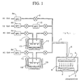
- a film forming system which is used to form a fluorine - containing silicon oxide film according to an embodiment of the present invention will be explained at first hereinafter with reference to FIG.1.
- FIG.1 is a schematic view showing a configuration of a thermal CVD apparatus comprising a reaction gas supplying section and a film forming section.
- a wafer loading table 2 having a built-in heater therein and a gas discharging portion 3 are furnished with a film forming chamber 1.
- An exhaust port 4 and a gas introducing port 5 are provided in the film forming chamber 1.
- Reaction gas is introduced from the gas introducing port 5 into the film forming chamber 1 via a pipe 7 while unnecessary reaction gas is exhausted from the exhaust port 4 to the outside of the film forming chamber 1.
- Mixed reaction gas is supplied to the pipe 7 from the reaction gas supplying portion.
- the reaction gas supplying portion is equipped with a plurality of branch pipes which are connected to respective gas sources corresponding to gas to be used.
- the branch pipes comprise a first branch pipe for supplying nitrogen gas, a second branch pipe for supplying ozone (O 3 ) containing oxygen gas, a third branch pipe for supplying organic silane with Si-F bond, e.g., fluorotriethoxysilane (F-TES), and a fourth branch pipe for supplying organic silane without Si-F bond, e.g., tetraethoxysilane (TEOS).
- F-TES fluorotriethoxysilane
- TEOS tetraethoxysilane
- a port for introducing nitrogen gas a mass flow controller (MFC) 8a, and a switching valve 9 which may cut off/introduce gas flow.
- MFC mass flow controller
- a switching valve 9 which may cut off/introduce gas flow.
- MFC mass flow controller
- the ozone generating unit 10 may convert oxygen gas into ozone in proper quantity so as to adjust the ozone density in oxygen gas.
- Nitrogen gas including F-TES in virtue of bubbling of the carrier gas (nitrogen gas) can be supplied to the pipe 7.
- a mass flow controller (MFC) 8d In the middle of the fourth branch pipe between a port for introducing carrier gas (nitrogen gas) and the pipe 7 are interposed a mass flow controller (MFC) 8d, a container 14 containing TEOS solution 16 therein, a heater 15 for heating the TEOS solution 16, and switching valves 9 which may cut off/introduce gas flow. Nitrogen gas including TEOS in virtue of bubbling of the carrier gas (nitrogen gas) can be supplied to the pipe 7.
- FIG.1 there will be explained a method for forming the fluorine - containing silicon oxide film according to the embodiment of the present invention based on an atmospheric pressure CVD method.
- a wafer 6 is placed on the wafer loading table 2 positioned at the bottom of the film forming chamber 1 and then heated.
- the temperature of the wafer 6 is varied film by film within the range of 100 to 350 °C.
- the F-TES solution 13 is heated and then held at the temperature of 40 °C.
- the TEOS solution 16 is heated and then held at the temperature of 65 °C.
- nitrogen gas is supplied at flow rate of 18 SLM to the pipe 7 via the first branch pipe
- oxygen gas including ozone by 2.4 % is supplied at flow rate of 7.5 SLM to the pipe 7 via the second branch pipe
- nitrogen gas including F-TES is supplied to the pipe 7 via the third branch pipe
- nitrogen gas including TEOS is supplied at flow rate of 2.0 SLM to the pipe 7 via the fourth branch pipe.
- FIG.3 shows a correlation of the deposition rate with the deposition temperature.
- An ordinate represents the deposition rate (nm/min) in linear scale while an abscissa represents the deposition temperature (°C) in linear scale.
- the flow rate of F-TES is kept constant at 2.0 SLM. As shown in FIG.3, the deposition rate assumes its maximum value of about 250 nm/min at almost 250 °C.
- FIG.5 shows a relationship between the refractive index of the fluorine - containing silicon oxide film obtained and the deposition temperature.
- An ordinate represents the refractive index in linear scale while an abscissa represents the deposition temperature (°C) in linear scale.
- the flow rate of F-TES is maintained constant at 2.0 SLM.
- the refractive index is about 1.385 at the deposition temperature of 180 °C.
- the refractive index is then increased linearly with the increase in the deposition temperature.
- the refractive index becomes about 1.425 at the substrate temperature of 350 °C.
- FIG.4 A relationship between the flow rate of F-TES and the deposition rate is shown in FIG.4.
- An ordinate represents the deposition rate (nm/min) in linear scale while an abscissa represents the flow rate of F-TES (SLM) in linear scale.
- the substrate temperature is held constant at 280 °C.
- the deposition rate is increased linearly with the increase in flow rate of F-TES, and the deposition rate reaches about 230 nm/min at the flow rate of F-TES of 3.0 SLM.
- FIG.6 shows a relationship between the refractive index of the fluorine - containing silicon oxide film formed and the flow rate of F-TES.
- An ordinate represents the refractive index in linear scale while an abscissa represents the flow rate of F-TES (SLM) in linear scale.
- the substrate temperature is kept constant at 280 °C.
- the refractive index is about 1.42 at the flow rate of F-TES of 0.5 SLM.
- the refractive index is then decreased gradually with the increase in the flow rate of F-TES.
- the refractive index becomes about 1.36 at the flow rate of F-TES of 3.0 SLM.
- relative dielectric constant can be controlled according to an amount of contained fluorine. In general, the more an amount of contained fluorine, the lower the relative dielectric constant. Since the fluorine - containing silicon oxide film is formed by thermal CVD method, it is superior in step coverage.
- the wafer 6 on which the fluorine - containing silicon oxide film is formed is placed on the wafer loading table 18 of the plasma processing apparatus.
- the wafer 6 is then heated and thereafter maintained at 370 °C.
- an electric power of 400 W having a frequency of 13.56 MHz is applied from a power source 22 to an upper electrode 19, and at the same time an electric power of 400 W having a frequency of 100 kHz is applied from a power source 23 to a lower electrode 18. Consequently, the gas is plasmanized and the wafer 6 is biased negatively, so that the fluorine - containing silicon oxide film formed on the wafer 6 is subjected to irradiation of plasma 24. After about 300 sec is elapsed, plasma irradiation is ceased and then the wafer 6 is taken out of the chamber 17.
- FIG.7 the measured results of the infrared absorption characteristics after plasma irradiation are shown in FIG.7.
- An ordinate represents the absorption intensity in arbitrary unit while an abscissa represents the number of wave (cm -1 ) in linear scale.
- Three kinds of measured results i.e., results obtained immediately after film formation, after plasma irradiation for 180 sec, and 300 sec, are compared with each other in FIG.7.
- the relative dielectric constant ⁇ can be lowered by enhancing a mixing ratio of the organic silane including fluorine to the organic silane including no fluorine to show the value of 3.2 to 3.4 after the plasma irradiation is carried out. Even in the event that the mixing ratio is enhanced, the silicon oxide film still has the large relative dielectric constant ⁇ unless the plasma irradiation is carried out.
- the process gas using oxygen gas is of advantage to the small relative dielectric constant rather than that using nitrogen gas.
- the relative dielectric constant may be lowered much more and advantage derived from included fluorine may be enhanced much more if the plasma process is carried out after film formation.
- fluorotriethoxysilane which is fluoroalkoxysilane has been used as organic silane having Si-F bond.
- TEOS or TES which is alkoxysilane has been used in the above embodiment as organic silane having no Si-F bond.
- R is alkyl group, aryl group, or their derivative
- the fluorine - containing silicon oxide film is formed by thermal CVD method using organic silane having Si-F bond as a source gas.
- the relative dielectric constant of the fluorine - containing silicon oxide film formed as mentioned above can be controlled by adjusting an amount of contained fluorine. In general, the more an amount of contained fluorine, the lower the-relative dielectric constant. Since the fluorine - containing silicon oxide film is formed by thermal CVD method, it is superior in step coverage.
Landscapes
- Chemical & Material Sciences (AREA)
- Inorganic Chemistry (AREA)
- General Chemical & Material Sciences (AREA)
- Chemical Kinetics & Catalysis (AREA)
- Engineering & Computer Science (AREA)
- Materials Engineering (AREA)
- Mechanical Engineering (AREA)
- Metallurgy (AREA)
- Organic Chemistry (AREA)
- Formation Of Insulating Films (AREA)
- Chemical Vapour Deposition (AREA)
Claims (6)
- Verfahren zur Bildung eines Films, umfassend die Schritte des Bildens eines Fluor-enthaltenden Siliziumoxidfilms auf einem Substrat (6) mittels thermischer Reaktion eines gemischten Gases, während das Substrat (6) erwärmt wird, wobei das gemischte Gas ein organisches Silan mit einer Si-F-Bindung, organisches Silan ohne Si-F-Bindung und ein Ozon-enthaltendes Gas umfasst; und Exponieren des Fluor-enthaltenen Siliziumoxidfilms an ein Plasma, enthaltend mindestens eines von Sauerstoff und Stickstoff, unter der Bedingung, bei der das Substrat erwärmt wird, nachdem der Fluor-enthaltende Siliziumoxidfilm auf dem Substrat gebildet worden ist.
- Verfahren zur Bildung eines Films gemäß Anspruch 1, worin der Fluor-enthaltende Siliziumoxidfilm bei atmosphärischem Druck gebildet wird.
- Verfahren zur Bildung eines Films gemäß Anspruch 1 oder 2, worin das organische Silan mit Si-F-Bindung zusammengesetzt ist aus Fluoralkoxysilan (SiFn(OR)4-n, n=1 bis 3, R ist eine Alkylgruppe, Arylgruppe oder deren Derivat), Fluoralkylsilan (SiFnR4-n, n=1 bis 3, R ist eine Alkylgruppe, Arylgruppe oder deren Derivat), einem Kettenfluorsiloxan (RnF3-nSiO(RkF2- kSiO)mSiF3-nRn, n=1, 2, k=0 bis 2, m≥0, R ist eine Alkylgruppe, Arylgruppe oder deren Derivat) oder einem ringförmigen Fluorsiloxan ((RkF2-kSiO)m, k=1, m≥2, R ist eine Alkylgruppe, Arylgruppe oder deren Derivat).
- Verfahren zur Bildung eines Films gemäß Anspruch 1 oder 2, worin das organische Silan ohne Si-F-Bindung zusammengesetzt ist aus Alkoxysilan (SiHn(OR)4-n, n=1 to 3, R ist eine Alkylgruppe, Arylgruppe oder deren Derivat), Alkylsilan (SiHnR4-n, n=1 bis 3, R ist eine Alkylgruppe, Arylgruppe oder deren Derivat), einem Kettensiloxan (RnH3-nSiO(RkH2-kSiO)mSiH3-nRn, n=1, 2, k=0 bis 2, m≥0, R ist eine Alkylgruppe, Arylgruppe oder deren Derivat), oder einem ringförmigen Siloxan ((RkH2-kSiO)m, k=1, m≥2, R ist eine Alkylgruppe, Arylgruppe oder deren Derivat).
- Verfahren zur Bildung eines Films gemäß Anspruch 1, 2, 3 oder 4, worin das Ozon-enthaltende Gas zusammengesetzt ist aus Ozon (03) und Sauerstoff (O2).
- Verfahren zur Bildung eines Films gemäß Anspruch 1, worin das Plasma, enthaltend mindestens eines von Sauerstoff und Stickstoff, ein Plasma von O2, NO, NO2 oder N2O ist.
Applications Claiming Priority (3)
| Application Number | Priority Date | Filing Date | Title |
|---|---|---|---|
| JP21089695 | 1995-08-18 | ||
| JP7210896A JP3061255B2 (ja) | 1995-08-18 | 1995-08-18 | 成膜方法 |
| JP210896/95 | 1995-08-18 |
Publications (2)
| Publication Number | Publication Date |
|---|---|
| EP0761841A1 EP0761841A1 (de) | 1997-03-12 |
| EP0761841B1 true EP0761841B1 (de) | 2002-06-12 |
Family
ID=16596880
Family Applications (1)
| Application Number | Title | Priority Date | Filing Date |
|---|---|---|---|
| EP96112891A Expired - Lifetime EP0761841B1 (de) | 1995-08-18 | 1996-08-09 | Verfahren zur Herstellung einer Schicht |
Country Status (5)
| Country | Link |
|---|---|
| US (1) | US5800877A (de) |
| EP (1) | EP0761841B1 (de) |
| JP (1) | JP3061255B2 (de) |
| KR (1) | KR100262053B1 (de) |
| DE (1) | DE69621723T2 (de) |
Cited By (1)
| Publication number | Priority date | Publication date | Assignee | Title |
|---|---|---|---|---|
| US8703625B2 (en) | 2010-02-04 | 2014-04-22 | Air Products And Chemicals, Inc. | Methods to prepare silicon-containing films |
Families Citing this family (53)
| Publication number | Priority date | Publication date | Assignee | Title |
|---|---|---|---|---|
| US6042901A (en) * | 1996-02-20 | 2000-03-28 | Lam Research Corporation | Method for depositing fluorine doped silicon dioxide films |
| JP3178375B2 (ja) * | 1997-06-03 | 2001-06-18 | 日本電気株式会社 | 絶縁膜の形成方法 |
| US5908672A (en) * | 1997-10-15 | 1999-06-01 | Applied Materials, Inc. | Method and apparatus for depositing a planarized passivation layer |
| US6337102B1 (en) | 1997-11-17 | 2002-01-08 | The Trustees Of Princeton University | Low pressure vapor phase deposition of organic thin films |
| US6303523B2 (en) | 1998-02-11 | 2001-10-16 | Applied Materials, Inc. | Plasma processes for depositing low dielectric constant films |
| US6660656B2 (en) | 1998-02-11 | 2003-12-09 | Applied Materials Inc. | Plasma processes for depositing low dielectric constant films |
| US6593247B1 (en) * | 1998-02-11 | 2003-07-15 | Applied Materials, Inc. | Method of depositing low k films using an oxidizing plasma |
| US6287990B1 (en) | 1998-02-11 | 2001-09-11 | Applied Materials, Inc. | CVD plasma assisted low dielectric constant films |
| US6054379A (en) | 1998-02-11 | 2000-04-25 | Applied Materials, Inc. | Method of depositing a low k dielectric with organo silane |
| US7804115B2 (en) | 1998-02-25 | 2010-09-28 | Micron Technology, Inc. | Semiconductor constructions having antireflective portions |
| US6274292B1 (en) | 1998-02-25 | 2001-08-14 | Micron Technology, Inc. | Semiconductor processing methods |
| US6667553B2 (en) | 1998-05-29 | 2003-12-23 | Dow Corning Corporation | H:SiOC coated substrates |
| US6159871A (en) | 1998-05-29 | 2000-12-12 | Dow Corning Corporation | Method for producing hydrogenated silicon oxycarbide films having low dielectric constant |
| US6153509A (en) * | 1998-07-01 | 2000-11-28 | Kabushiki Kaisha Toshiba | Method of manufacturing a semiconductor device |
| US6383951B1 (en) * | 1998-09-03 | 2002-05-07 | Micron Technology, Inc. | Low dielectric constant material for integrated circuit fabrication |
| US6281100B1 (en) | 1998-09-03 | 2001-08-28 | Micron Technology, Inc. | Semiconductor processing methods |
| US6268282B1 (en) * | 1998-09-03 | 2001-07-31 | Micron Technology, Inc. | Semiconductor processing methods of forming and utilizing antireflective material layers, and methods of forming transistor gate stacks |
| US6727190B2 (en) * | 1998-09-03 | 2004-04-27 | Micron Technology, Inc. | Method of forming fluorine doped boron-phosphorous silicate glass (F-BPSG) insulating materials |
| US6323101B1 (en) | 1998-09-03 | 2001-11-27 | Micron Technology, Inc. | Semiconductor processing methods, methods of forming silicon dioxide methods of forming trench isolation regions, and methods of forming interlevel dielectric layers |
| US6828683B2 (en) | 1998-12-23 | 2004-12-07 | Micron Technology, Inc. | Semiconductor devices, and semiconductor processing methods |
| US7235499B1 (en) | 1999-01-20 | 2007-06-26 | Micron Technology, Inc. | Semiconductor processing methods |
| WO2000051174A1 (en) | 1999-02-26 | 2000-08-31 | Trikon Holdings Limited | A method of processing a polymer layer |
| JP4515550B2 (ja) * | 1999-03-18 | 2010-08-04 | 東芝モバイルディスプレイ株式会社 | 薄膜形成方法 |
| JP2003503849A (ja) | 1999-06-26 | 2003-01-28 | トリコン ホールディングス リミティド | 基材上にフィルムを形成する方法及び装置 |
| US7067414B1 (en) | 1999-09-01 | 2006-06-27 | Micron Technology, Inc. | Low k interlevel dielectric layer fabrication methods |
| DE19960092A1 (de) * | 1999-12-14 | 2001-07-12 | Bosch Gmbh Robert | Beschichtungsverfahren |
| US6440860B1 (en) | 2000-01-18 | 2002-08-27 | Micron Technology, Inc. | Semiconductor processing methods of transferring patterns from patterned photoresists to materials, and structures comprising silicon nitride |
| JP3934343B2 (ja) * | 2000-07-12 | 2007-06-20 | キヤノンマーケティングジャパン株式会社 | 半導体装置及びその製造方法 |
| US6531398B1 (en) | 2000-10-30 | 2003-03-11 | Applied Materials, Inc. | Method of depositing organosillicate layers |
| KR20020051456A (ko) * | 2000-12-22 | 2002-06-29 | 황 철 주 | 저온환경의 화학기상증착 방법 |
| US6709721B2 (en) | 2001-03-28 | 2004-03-23 | Applied Materials Inc. | Purge heater design and process development for the improvement of low k film properties |
| US6732551B2 (en) | 2001-05-04 | 2004-05-11 | Corning Incorporated | Method and feedstock for making silica |
| US7074489B2 (en) * | 2001-05-23 | 2006-07-11 | Air Products And Chemicals, Inc. | Low dielectric constant material and method of processing by CVD |
| US6716770B2 (en) * | 2001-05-23 | 2004-04-06 | Air Products And Chemicals, Inc. | Low dielectric constant material and method of processing by CVD |
| US6486082B1 (en) | 2001-06-18 | 2002-11-26 | Applied Materials, Inc. | CVD plasma assisted lower dielectric constant sicoh film |
| KR20030001959A (ko) * | 2001-06-28 | 2003-01-08 | 주식회사 하이닉스반도체 | 반도체 소자의 제조 방법 |
| US6936309B2 (en) | 2002-04-02 | 2005-08-30 | Applied Materials, Inc. | Hardness improvement of silicon carboxy films |
| US20030194495A1 (en) * | 2002-04-11 | 2003-10-16 | Applied Materials, Inc. | Crosslink cyclo-siloxane compound with linear bridging group to form ultra low k dielectric |
| US20030211244A1 (en) * | 2002-04-11 | 2003-11-13 | Applied Materials, Inc. | Reacting an organosilicon compound with an oxidizing gas to form an ultra low k dielectric |
| US20030194496A1 (en) * | 2002-04-11 | 2003-10-16 | Applied Materials, Inc. | Methods for depositing dielectric material |
| US6815373B2 (en) * | 2002-04-16 | 2004-11-09 | Applied Materials Inc. | Use of cyclic siloxanes for hardness improvement of low k dielectric films |
| US20030206337A1 (en) * | 2002-05-06 | 2003-11-06 | Eastman Kodak Company | Exposure apparatus for irradiating a sensitized substrate |
| US6927178B2 (en) | 2002-07-11 | 2005-08-09 | Applied Materials, Inc. | Nitrogen-free dielectric anti-reflective coating and hardmask |
| US7105460B2 (en) | 2002-07-11 | 2006-09-12 | Applied Materials | Nitrogen-free dielectric anti-reflective coating and hardmask |
| US6897163B2 (en) | 2003-01-31 | 2005-05-24 | Applied Materials, Inc. | Method for depositing a low dielectric constant film |
| US7288205B2 (en) | 2004-07-09 | 2007-10-30 | Applied Materials, Inc. | Hermetic low dielectric constant layer for barrier applications |
| US7425350B2 (en) * | 2005-04-29 | 2008-09-16 | Asm Japan K.K. | Apparatus, precursors and deposition methods for silicon-containing materials |
| JP2009538989A (ja) * | 2006-05-30 | 2009-11-12 | フジフィルム マニュファクチャリング ユーロプ ビー.ブイ. | パルス化大気圧グロー放電を使用する堆積の方法及び装置 |
| US8338307B2 (en) * | 2007-02-13 | 2012-12-25 | Fujifilm Manufacturing Europe B.V. | Substrate plasma treatment using magnetic mask device |
| JP5084343B2 (ja) * | 2007-05-07 | 2012-11-28 | 株式会社半導体エネルギー研究所 | 半導体装置の作製方法 |
| WO2009096785A1 (en) * | 2008-02-01 | 2009-08-06 | Fujifilm Manufacturing Europe B.V. | Method and apparatus for plasma surface treatment of a moving substrate |
| CN101661962B (zh) * | 2008-08-29 | 2012-05-09 | 苏州中来光伏新材股份有限公司 | 一种具有高粘结性的太阳能电池背膜及加工工艺 |
| KR101354742B1 (ko) * | 2011-06-30 | 2014-01-22 | 가부시끼가이샤 도시바 | 템플릿 기판 및 그 제조 방법 |
Family Cites Families (13)
| Publication number | Priority date | Publication date | Assignee | Title |
|---|---|---|---|---|
| US4737379A (en) * | 1982-09-24 | 1988-04-12 | Energy Conversion Devices, Inc. | Plasma deposited coatings, and low temperature plasma method of making same |
| JPH04167431A (ja) * | 1990-10-31 | 1992-06-15 | Handotai Process Kenkyusho:Kk | 半導体装置の製造方法 |
| DE69130947T2 (de) * | 1991-01-08 | 1999-07-08 | Fujitsu Ltd., Kawasaki, Kanagawa | Verfahren zur bildung eines siliciumoxid-filmes |
| JP2699695B2 (ja) * | 1991-06-07 | 1998-01-19 | 日本電気株式会社 | 化学気相成長法 |
| JPH05226480A (ja) * | 1991-12-04 | 1993-09-03 | Nec Corp | 半導体装置の製造方法 |
| JP2773530B2 (ja) * | 1992-04-15 | 1998-07-09 | 日本電気株式会社 | 半導体装置の製造方法 |
| EP0572704B1 (de) * | 1992-06-05 | 2000-04-19 | Semiconductor Process Laboratory Co., Ltd. | Verfahren zur Herstellung einer Halbleiteranordnung mittels eines Verfahren zur Reformierung einer Isolationsschicht die bei niederiger Temperatur durch CVD hergestellt ist |
| JP3688726B2 (ja) * | 1992-07-17 | 2005-08-31 | 株式会社東芝 | 半導体装置の製造方法 |
| JPH06132276A (ja) * | 1992-10-22 | 1994-05-13 | Kawasaki Steel Corp | 半導体膜形成方法 |
| JPH0750295A (ja) * | 1993-08-05 | 1995-02-21 | Fujitsu Ltd | 半導体装置の製造方法 |
| JPH07193004A (ja) * | 1993-11-22 | 1995-07-28 | Applied Materials Inc | 半導体装置の薄膜形成方法 |
| JPH07161705A (ja) * | 1993-12-03 | 1995-06-23 | Nec Corp | 半導体装置の多層配線層間絶縁膜の形成方法 |
| JP2899600B2 (ja) * | 1994-01-25 | 1999-06-02 | キヤノン販売 株式会社 | 成膜方法 |
-
1995
- 1995-08-18 JP JP7210896A patent/JP3061255B2/ja not_active Expired - Lifetime
-
1996
- 1996-08-09 US US08/694,660 patent/US5800877A/en not_active Expired - Fee Related
- 1996-08-09 DE DE69621723T patent/DE69621723T2/de not_active Expired - Fee Related
- 1996-08-09 KR KR1019960033147A patent/KR100262053B1/ko not_active Expired - Fee Related
- 1996-08-09 EP EP96112891A patent/EP0761841B1/de not_active Expired - Lifetime
Cited By (1)
| Publication number | Priority date | Publication date | Assignee | Title |
|---|---|---|---|---|
| US8703625B2 (en) | 2010-02-04 | 2014-04-22 | Air Products And Chemicals, Inc. | Methods to prepare silicon-containing films |
Also Published As
| Publication number | Publication date |
|---|---|
| US5800877A (en) | 1998-09-01 |
| JPH0964029A (ja) | 1997-03-07 |
| KR970013003A (ko) | 1997-03-29 |
| DE69621723D1 (de) | 2002-07-18 |
| EP0761841A1 (de) | 1997-03-12 |
| DE69621723T2 (de) | 2002-11-28 |
| JP3061255B2 (ja) | 2000-07-10 |
| KR100262053B1 (ko) | 2000-07-15 |
Similar Documents
| Publication | Publication Date | Title |
|---|---|---|
| EP0761841B1 (de) | Verfahren zur Herstellung einer Schicht | |
| US5356722A (en) | Method for depositing ozone/TEOS silicon oxide films of reduced surface sensitivity | |
| US5869149A (en) | Method for preparing nitrogen surface treated fluorine doped silicon dioxide films | |
| KR100308447B1 (ko) | 기판상에 층을 증착시키는 방법 | |
| US5648175A (en) | Chemical vapor deposition reactor system and integrated circuit | |
| US6077574A (en) | Plasma CVD process for forming a fluorine-doped SiO2 dielectric film | |
| US6090167A (en) | Method and apparatus for improving film stability of halogen-doped silicon oxide films | |
| US5376591A (en) | Method for manufacturing semiconductor device | |
| EP0934433B1 (de) | Verfahren zur abscheidung von fluor-dotierten siliziumdioxidschichten | |
| US5763018A (en) | Method for forming dielectric layer | |
| JP3701626B2 (ja) | 半導体装置の製造方法 | |
| KR100368100B1 (ko) | 불소첨가절연막의형성방법 | |
| JP2001267315A (ja) | 高密度プラズマリアクタにおける窒化ケイ素のインサイチュ(insitu)堆積及び集積化 | |
| EP1217648A2 (de) | Verfahren zur Herstellung einer dielektrischen Zwischenschicht mit niedriger Dielektrizitätskonstante | |
| US6345589B1 (en) | Method and apparatus for forming a borophosphosilicate film | |
| EP1284500A2 (de) | Halbleitervorrichtung und Verfahren zu deren Herstellung | |
| EP1432843B1 (de) | Verfahren zur herstellung eines films aus kohlenstoffdotiertem oxid | |
| US6291028B1 (en) | Method and apparatus for improving the film quality of plasma enhanced CVD films at the interface | |
| JP3934343B2 (ja) | 半導体装置及びその製造方法 | |
| EP0759481A1 (de) | Verfahren zum Abscheiden eines stabilen Films aus fluoriertem TEOS | |
| JP2001332550A (ja) | 半導体装置及びその製造方法 | |
| EP0730298A2 (de) | Dielektricum, Herstellungsverfahren, sowie Halbleitervorrichtung unter Verwendung von diesem Dielektricum | |
| JP3749162B2 (ja) | 半導体装置の製造方法 | |
| US5569499A (en) | Method for reforming insulating film | |
| Rieger et al. | ArF laser induced CVD of SiO2 films: a search for the best suitable precursors |
Legal Events
| Date | Code | Title | Description |
|---|---|---|---|
| PUAI | Public reference made under article 153(3) epc to a published international application that has entered the european phase |
Free format text: ORIGINAL CODE: 0009012 |
|
| AK | Designated contracting states |
Kind code of ref document: A1 Designated state(s): DE GB NL |
|
| 17P | Request for examination filed |
Effective date: 19970416 |
|
| 17Q | First examination report despatched |
Effective date: 19991004 |
|
| GRAG | Despatch of communication of intention to grant |
Free format text: ORIGINAL CODE: EPIDOS AGRA |
|
| GRAG | Despatch of communication of intention to grant |
Free format text: ORIGINAL CODE: EPIDOS AGRA |
|
| GRAH | Despatch of communication of intention to grant a patent |
Free format text: ORIGINAL CODE: EPIDOS IGRA |
|
| GRAH | Despatch of communication of intention to grant a patent |
Free format text: ORIGINAL CODE: EPIDOS IGRA |
|
| GRAA | (expected) grant |
Free format text: ORIGINAL CODE: 0009210 |
|
| AK | Designated contracting states |
Kind code of ref document: B1 Designated state(s): DE GB NL |
|
| REG | Reference to a national code |
Ref country code: GB Ref legal event code: FG4D |
|
| REF | Corresponds to: |
Ref document number: 69621723 Country of ref document: DE Date of ref document: 20020718 |
|
| PLBE | No opposition filed within time limit |
Free format text: ORIGINAL CODE: 0009261 |
|
| STAA | Information on the status of an ep patent application or granted ep patent |
Free format text: STATUS: NO OPPOSITION FILED WITHIN TIME LIMIT |
|
| 26N | No opposition filed |
Effective date: 20030313 |
|
| PGFP | Annual fee paid to national office [announced via postgrant information from national office to epo] |
Ref country code: NL Payment date: 20030728 Year of fee payment: 8 Ref country code: GB Payment date: 20030728 Year of fee payment: 8 |
|
| PGFP | Annual fee paid to national office [announced via postgrant information from national office to epo] |
Ref country code: DE Payment date: 20030805 Year of fee payment: 8 |
|
| PG25 | Lapsed in a contracting state [announced via postgrant information from national office to epo] |
Ref country code: GB Free format text: LAPSE BECAUSE OF NON-PAYMENT OF DUE FEES Effective date: 20040809 |
|
| PG25 | Lapsed in a contracting state [announced via postgrant information from national office to epo] |
Ref country code: NL Free format text: LAPSE BECAUSE OF NON-PAYMENT OF DUE FEES Effective date: 20050301 Ref country code: DE Free format text: LAPSE BECAUSE OF NON-PAYMENT OF DUE FEES Effective date: 20050301 |
|
| GBPC | Gb: european patent ceased through non-payment of renewal fee |
Effective date: 20040809 |
|
| NLV4 | Nl: lapsed or anulled due to non-payment of the annual fee |
Effective date: 20050301 |