EP0765097A2 - Optisches Vermittlungssystem für optische Wellenlängen- und Zeitmultiplexsignale - Google Patents
Optisches Vermittlungssystem für optische Wellenlängen- und Zeitmultiplexsignale Download PDFInfo
- Publication number
- EP0765097A2 EP0765097A2 EP96117346A EP96117346A EP0765097A2 EP 0765097 A2 EP0765097 A2 EP 0765097A2 EP 96117346 A EP96117346 A EP 96117346A EP 96117346 A EP96117346 A EP 96117346A EP 0765097 A2 EP0765097 A2 EP 0765097A2
- Authority
- EP
- European Patent Office
- Prior art keywords
- optical
- wavelength
- division
- signal
- time
- Prior art date
- Legal status (The legal status is an assumption and is not a legal conclusion. Google has not performed a legal analysis and makes no representation as to the accuracy of the status listed.)
- Withdrawn
Links
- 230000003287 optical effect Effects 0.000 title claims abstract description 345
- 230000015654 memory Effects 0.000 claims description 50
- 230000000875 corresponding effect Effects 0.000 description 25
- 230000007423 decrease Effects 0.000 description 16
- 238000010586 diagram Methods 0.000 description 6
- 230000002596 correlated effect Effects 0.000 description 5
- 230000005540 biological transmission Effects 0.000 description 4
- 230000001276 controlling effect Effects 0.000 description 3
- 230000007704 transition Effects 0.000 description 3
- 239000013307 optical fiber Substances 0.000 description 2
- 239000000969 carrier Substances 0.000 description 1
- 239000002131 composite material Substances 0.000 description 1
- 238000010276 construction Methods 0.000 description 1
- 230000003247 decreasing effect Effects 0.000 description 1
- 230000000694 effects Effects 0.000 description 1
- 238000001914 filtration Methods 0.000 description 1
- 230000006870 function Effects 0.000 description 1
- 239000000463 material Substances 0.000 description 1
- 230000005693 optoelectronics Effects 0.000 description 1
- 239000007787 solid Substances 0.000 description 1
Images







Classifications
-
- H—ELECTRICITY
- H04—ELECTRIC COMMUNICATION TECHNIQUE
- H04Q—SELECTING
- H04Q11/00—Selecting arrangements for multiplex systems
- H04Q11/0001—Selecting arrangements for multiplex systems using optical switching
- H04Q11/0005—Switch and router aspects
-
- H—ELECTRICITY
- H04—ELECTRIC COMMUNICATION TECHNIQUE
- H04Q—SELECTING
- H04Q11/00—Selecting arrangements for multiplex systems
- H04Q11/0001—Selecting arrangements for multiplex systems using optical switching
- H04Q11/0005—Switch and router aspects
- H04Q2011/0007—Construction
- H04Q2011/002—Construction using optical delay lines or optical buffers or optical recirculation
Definitions
- This invention relates to an optical switching system for optcal wavelength-division and time-division multiplexed signals, and more particularly to, an optical switching system for optical wavelength-division and time division multiplexed signals in which input and output optical signals are directly exchanged each other without being converted to electric signals.
- An optical communication system using an optical fiber as a transmission line has advantages such as a transmission ability of mass information due to a broadband characteristic of the optical fiber or a low induced noise transmission ability. Therefore, such an optical communication system will be used widely in various fields.
- an optical switching system for optical wavelength-division and time-division multiplexed signals is used in which an input optical signal having a specific wavelength in a specific time slot is exchanged to be an output optical signal having a different wavelength in a different time slot. It is preferable to exchange signals without converting to electric signals in the switching system.
- a first conventional optical switching system has been disclosed by Suzuki et al. on pages 91 to 96 of the text SE87-146 of Switching Engineering Conference of Electronics and Information Communication, entitled “A Study on Wavelength-Division and Time-Division Composite Optical Communication Networks", 1987.
- optical wavelength-division and time-division multiplexed signals are exchanged by converting wavelengths and time slots of the input optical signals.
- the first conventional optical switching system includes an optical splitter which divides an input optical signal to a plurality of optical signals, a plurality of tunable wavelength filters each of which selects one optical signal having a desired wavelength and a time slot, a plurality of optical bistable elements each of which converts a wavelength of each corresponding optical signal to a predetermined wavelength, and an optical switch which selectively supplies a selected signal from the converted signals supplied from the corresponding optical bistable element.
- the optical bistable element can hold the output intensity P out for a desired period by controlling conditions of the input intensity P in and the injected current i.
- Such an optical bistable element has been disclosed on pages 1088 and 1089 of Electronics Letters, No. 20, Vol. 23, September, 24, 1987.
- the optical switch includes a plurality of optical gate switches.
- the optical splitter supplies the tunable wavelength filters with divided input signals which are optical wavelength-division and time-division multiplexed signals.
- One of the tunable wavelength filters selects a signal having a desired wavelength from the optical wavelength-division and time-division multiplexed signals.
- the optical bistable elements are supplied with the current i which decreases to be reset periodically. If a signal having a specific wavelength allocated in a specific time slot is supplied to one of the optical bistable elements, the optical bistable element keeps supplying the optical switch with an output signal corresponding to the signal supplied thereto but converted to have a different predetermined wavelength for a period until the current i decreases.
- the optical switch supplies an optical output port with the output signal supplied from the optical bistable element in a desired time slot. Therefore, the input signal is exchanged to be an output signal having a different wavelength in a different time slot.
- the second conventional optical switching system includes a wavelength filter which selects one optical signal having a predetermined wavelength from an input signal which is an optical wavelength-division and time-division multiplexed signal, an optical switch which selectively supplies a plurality of signals each of which is allocated in a different time slot, a plurality of tunable wavelength output optical bistable elements each of which converts a wavelength of each corresponding optical signal to a desired wavelength and keeps supplying the converted signal for a period, and an optical switch each of which selectively supplies a plurality of signals each of which is allocated in a different time slot in turn.
- Structures of the optical bistable elements and the optical switch in the second conventional optical switching system are the same as those of the optical bistable elements and the optical switch in the first conventional optical switching system.
- the wavelength filter selects a signal having a predetermined wavelength from the optical wavelength-division and time-division multiplexed signals.
- the tunable wavelength output optical bistable elements are supplied with the current i which decreases periodically to be reset. If a signal having a specific wavelength allocated in a specific time slot is supplied to one of the optical bistable element, the optical bistable element keeps supplying the optical switch with an output signal corresponding to the signal supplied thereto but converted to have a different desired wavelength for a period until the current i decreases.
- the optical switch supplies the output signal supplied from the optical bistable element in a desired time slot. Therefore, the input signal is exchanged to be an output signal having a different wavelength in a different time slot.
- Each of the optical bistable elements keeps supplying an output signal until the current i decreases, so that the optical switch for reading out optical signals is required to include optical gate switches corresponding to each optical bistable element in order to supply the output signals in turn to an optical combiner.
- the optical bistable elements and the optical gate switches is m ⁇ n, respectively, so that required number of active elements is 3 ⁇ m ⁇ n .
- Fig. 1 shows the first conventional optical switching system which exchanges input and output optical signals which are divided to two wavelengths of ⁇ 1 and ⁇ 2 and divided to three time slots of T 1 to T 3 .
- the optical switching system includes an optical splitter 20 which divides an input optical signal to two optical signals, two optical splitters 31 and 32 each divides a divided optical signal supplied from the optical splitter 20 to three optical signals, six tunable wavelength filters 41 to 46 each selects one optical signal having a specific wavelength and a time slot, six optical bistable elements 51 to 56 each converts a wavelength of each corresponding optical signal to ⁇ 1 in the elements 51 to 53 and ⁇ 2 in the elements 54 to 56 and maintains to supply the converted signal, two optical switches 61 and 62 each selectively supplies a selected signal from the converted signals supplied from the corresponding optical bistable element, and an optical combiner 70 which combines the selected signals supplied from the optical switches 61 and 62.
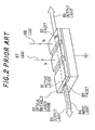
- Fig. 2 shows a structure of the optical bistable elements 51 to 56.
- the optical bistable element includes an optical bistable laser diode 80 including an active layer 81 indicated by dot lines.
- An input light 84 is supplied through a facet 82 of the active layer 81 and irradiated from the facet 82 and the opposite facet 83 as output lights 85 and 86, respectively.
- the optical bistable element is injected with a current i which is a sum of i 2 and i 3 which are supplied to the optical bistable laser diode 80 through leads 87 and 88, respectively.
- the wavelength of output lights 85 and 86 can be changed to a desired wavelength by changing a ratio of i 2 to i 3 while the whole current i is maintained to be constant. The wavelength thereof becomes shorter when the ratio i 2 /i 3 becomes large, while the wavelength becomes longer when the ratio i 2 /i 3 becomes small.
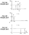
- Fig. 3A shows an output intensity P out correlated with an injected current i on a condition that an input intensity P in of the input light is zero.
- an output characteristic shows a hysteresis loop.
- an optical intensity P out of the output light remains almost zero as the injected current i increases from zero until i C , however, the optical intensity P out increases abruptly to P 1 when the injected current i becomes i t .
- the optical intensity P out remains P 1 as the injected current i decrease until i c , however, the optical intensity P out decreased abruptly to zero. Consequently, the optical bistable element has two stable points A and B of reset and set states at the injected current i b , respectively.
- Fig. 3B shows the output intensity P out correlated with an input intensity P in of the input light on a condition that the injected current i is fixed to i b .
- the optical intensity P out remains zero as the input intensity P in increases from zero until P in when the optical bistable element is at the reset state A, however, the optical intensity P out increases abruptly to P 1 when the input intensity P in becomes P tb .
- the optical intensity P out remains P 1 as the input intensity P in decreases, and the optical intensity P out remains P 1 even if the input intensity P in becomes zero when the optical bistable element becomes at the set state B.
- the optical bistable element which is initially at the reset state A becomes at the set state B where the output intensity P out is P 1 by supplying the input intensity P in larger than P tb , and the output intensity P out is maintained to P 1 even after stopping of the supply of the input intensity P in .
- Fig. 3C shows the output intensity P out correlated with the input intensity P in on a condition that the injected current i is fixed to i 0 smaller than i c .
- the optical intensity P out remains zero as the input intensity P in increases from zero until P t0 , however, the optical intensity P out increases abruptly to P 1 when the input intensity P in becomes P t0 .
- the optical intensity P out remains P 1 as the input intensity P in decreases until P d0 , however, the optical intensity P out decreases abruptly to zero when the input intensity P in becomes P d0 . Therefore, it is possible to change the states of the optical bistable element from at the set state B where the injected current i is i b to at the reset state A by changing the input intensity P in to zero and the injected current i to under i c .
- the optical bistable element can hold the output intensity P out for a desired period by controlling conditions of the input intensity P in and the injected current i.
- Fig. 4 shows a structure of the optical switches 61 and 62.
- the optical switch includes three optical gate switches 91 to 93 and an optical combiner 94.
- the optical gate switches 91 to 93 supply the optical combiner 94 with input signals which are supplied respectively from input ports 1 to 3 in accordance with a control signal supplied thereto.
- the optical bistable element 51 keeps supplying an output signal of wavelength ⁇ 2 corresponding to the input signal A to the optical switch 61 for the period until the current i decreases.
- the optical switch 61 supplies the output signal of wavelength ⁇ 1 in the time slot T 3 to the optical combiner 70, so that an output signal S 11 including a signal of wavelength ⁇ 1 in the time slot T 3 is supplied from the output port 11.
- Fig. 6 shows the second conventional optical switching system which exchanges input and output optical signals which are divided to two wavelengths of ⁇ 1 and ⁇ 2 and divided to three time slots of T 1 to T 3 .
- the optical switching system includes an optical splitter 100 which divides an input optical signal to two optical signals, two wavelength filters 111 and 112 each selects one optical signal having a specific wavelength, two optical write switches 121 and 122 each selectively supplies three signals in time slots T 1 to T 3 , six tunable wavelength output optical bistable elements 131 to 136 each converts a wavelength of each corresponding optical signal to ⁇ 1 in the elements 131 to 133 and ⁇ 2 in the elements 134 to 136 and maintains to supply the converted signal, two optical read switches 141 and 142 each selectively supplies a selected signal from the converted signals supplied from the corresponding [unable wavelength output optical bistable element, and an optical combiner 150 which combines the selected signals supplied from the optical switches 141 and 142.
- a structure of the optical bistable elements 131 to 136 is the same as shown in Fig. 2, and operation thereof is the same as explained before in the explanation of the first conventional optical switching system.
- a structure of the optical read switches 141 and 142 is the same as shown in Fig. 4.
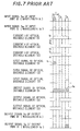
- Fig. 7 It is supposed that input signals S 01 and S 02 of wavelengths ⁇ 1 and ⁇ 2 allocated respectively into time slots T 1 to T 3 are supplied to an input port 13, and the input signal A of a wavelength ⁇ 1 in a time slot T 1 is to to be exchanged to be supplied to an output port 14 as an output signal S 14 of a wavelength ⁇ 2 in a time slot T 3 .
- the optical splitter 100 divides the input signal to two signals each to be supplied to the wavelength filters 111 and 112.
- the wavelength filters 111 and 112 supplies input signals S 03 of wavelength ⁇ 1 and S 04 of wavelength ⁇ 2 respectively to the optical write switches 121 and 122.
- the optical write switch 121 supplies the tunable wavelength output optical bistable elements 131 to 133 with input signals respectively allocated in the time slots T 1 to T 3 , respectively.
- the optical bistable elements 131 to 133 are supplied with the currents i each decreases periodically as shown in Fig. 7, so that the optical bistable elements 131 to 133 become at a reset state periodically in different timings. If the input signals in the time slots T 1 to T 3 are supplied to the optical bistable element 131 to 133, the optical bistable elements 131 to 133 keep supplying output signals of wavelengths ⁇ 1 corresponding to the input signals to the optical switch 141 for the period until the current i decreases.
- the optical switch 141 supplies the output signal of wavelength ⁇ 1 in the time slot T 3 to the optical combiner 150, so that an output signal S 14 including a signal of wavelength ⁇ 2 in the time slot T 3 is supplied from the output port 14.
- the optical switching system includes an optical splitter 200 which divides an input optical signal to two optical signals, two optical splitters 211 and 212 each divides a divided optical signal supplied from the optical splitter 200 to three optical signals, six tunable wavelength filters 221 to 226 each selects one optical signal having a specific wavelength and a time slot, six optical memories 231 to 236 each memories a signal supplied from the corresponding tunable wavelength filter, two optical combiners 241 and 242 each combines signals supplied from the optical memories 231 to 236, and an optical combiner 250 which combines the signals supplied from the optical combiners 241 and 242.
- Fig. 9 shows a structure of the optical memories 231 to 236.
- the optical memory includes an optical guide layer 281 having facets 282 and 283.
- An input light 284 is supplied through the facet 282 of the optical guide layer 281 and irradiated from both the facet 282 and the opposite facet 283 as output lights 284 and 285, respectively.
- the optical memory is applied with a control voltage V which controls the output characteristic thereof.
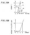
- Fig. 10A shows a current I which flows through the optical memory correlated with the control voltage V on condition that an input light P in is zero.
- V s V s
- After passing over V s there exist two pairs of stable points, that are a pair of A 1 and B 1 on a load line l 1 operated on one operation condition and another pair of A 2 and B 2 on a load line l 2 operated on another operation condition.
- Fig. 10B shows an output intensity P out of the optical memory correlated with the current I.
- the output intensity P out increases gradually as the current I increases from zero to I t , however, the output intensity P out increases abruptly when the current I becomes over I t .
- the optical memory has a threshold characteristic.
- the operation state of the optical memory transits from the stable point A 2 to the stable point B 2 when the control voltage V becomes V 2 which is lower than V s even if the control voltage V does not reach V s , and the current I 2 flows through the optical memory, so that the optical memory irradiates the output light of P 2 .
- the current I becomes zero when the control voltage V becomes zero, however, the current I becomes I 2 when the control voltage V becomes V 2 even if the input light intensity P in is zero.
- carriers exist in the optical memory These carries are generated when the control voltage V 2 is applied to the optical memory while the input light P in is supplied thereto.
- the optical memory can supply the output light P out corresponding to the input light P in at any time by applying the control voltage V 2 there to after experiencing the condition that the input light P in is not zero when the control voltage V s is applied thereto.
- the carries in the optical memory can be removed therefrom by applying the control voltage V having a negative value thereto, so that the optical memory becomes at an initial state in which the transition from the stable point A 2 to B 2 does not occur unless it is applied with the control voltage V higher than V s .
- the output light may affect the transition of the stable points A 2 to B 2 in case of memorizing the input light data.
- the control voltage V in the memorizing operation may be preferably V 1 by which the transition from the stable point A 1 to the stable point B 1 in which the current I 1 smaller than I t flows in the optical memory occurs, so that the output light intensity P out becomes P 1 which is quite small, as shown in Fig. 10B.
- the optical memory can memorize the output intensity P out , so that the optical memory can supply the output light P out corresponding to the input light P in at any time by applying the control voltage V 2 thereto after experiencing the condition that the input light P in is not zero when the control voltage V s is applied thereto.
- the wavelength of the output light P out of the optical memory can be changed by adjusting either the control voltage V b2 at the reading operation or the current I by adjusting a value of a resistance connected to the lead 286 through which the current I flows.
- the wavelength of the output light P out can be also changed by controlling the temperature of the optical memory.
- the optical memory 231 memorizes the data corresponding to the input signal A at the time slot T 1 in which the control voltage V rises to V b1 . Then, the optical memory 231 supplies the an output signal of wavelength ⁇ 1 corresponding to the input signal A at the time slot T 3 in which the control voltage V rises to V b2 .
- the optical combiner 241 combines output signals including the output signal supplied from the optical memory 231, and then the optical combiner 250 combines output signals from the optical combiners 241 and 242, so that an output signal S 16 including a signal of wavelength ⁇ 1 in the time slot T 3 is supplied from the output port 270.
- the optical memory can supply the output light P out corresponding to the input light P in at any time by applying the control voltage V 2 thereto, so that it is not necessary to be provided with optical switches in the system. Therefore, the number of active elements decreases to 2 ⁇ m ⁇ n in case of the wavelength-division of m and time-division multiplexity numbers of n.
- the optical switching system includes an optical splitter 300 which divides an input optical signal to two optical signals, two optical splitters 311 and 312 each divides a divided optical signal supplied from the optical splitter 300 to three optical signals, six wavelength filters 321 to 326 each selecting one optical signal having a specific wavelength and a time slot, six tunable wavelength optical memories 331 to 336 each memorizing a signal supplied from the corresponding wavelength filter, two optical combiners 341 and 342 each combines signals supplied from the tunable wavelength optical memories 331 to 336, and an optical combiner 350 which combines the signals supplied from the optical combiners 341 and 342.
- the structure of the tunable wavelength optical memories 331 to 336 is the same as shown in Fig. 9, and the operation thereof is also the same, except that each of the tunable wavelength optical memories can convert the wavelength of the input signal to desired wavelengths selected from ⁇ 1 and ⁇ 2 .
- the optical memory 331 becomes at a reset state periodically to clear the memorized data. If the input signal A of wavelength ⁇ 2 in a time slot T 1 is supplied to the optical memory 331, the optical memory 331 memorizes the data corresponding to the input signal A at the time slot T 1 in which the control voltage V rises to V b1 . Then, the optical memory 331 supplies the an output signal of wavelength ⁇ 1 corresponding to the input signal A at the time slot T 3 in which the control voltage V rises to V b2 .
- the optical combiner 341 combines output signals including the output signal supplied from the optical memory 331, and then the optical combiner 350 combines output signals from the optical combiners 341 and 342, so that an output signal S 18 including a signal of wavelength ⁇ 1 in the time slot T 3 is supplied from the output port 370.
- the optical switching system has two input ports and two output ports.
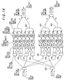
- the optical switching system includes two optical splitters 401 and 402 each dividing an input optical signal to two optical signals, eight optical splitters 411 and 318 each dividing a divided optical signal supplied from the optical splitters 401 or 402 to three optical signals, twelve optical switches 421 to 432 each selectively supplying an output optical signal from two input signals from the corresponding two optical splitters of the twelve optical splitters, twelve tunable wavelength filters 441 to 452 each selecting one optical signal having a specific wavelength and a time slot, twelve optical bistable elements 461 to 472 each keeps supplying a signal supplied from the corresponding tunable wavelength filter, four optical read switches 481 to 484 each selectively supplying an output signal selected from the signals supplied from the corresponding three optical bistable elements of the twelve optical bistable elements 461 to 472, and two optical
- the optical switch 421 is supplied with the input signal S 31 of wavelength ⁇ 1 from the input port 501 through the optical splitters 401 and 411 and S 32 of wavelength ⁇ 2 from the input port 502 through the optical splitters 402 and 412, and the optical switch 421 supplies output signals supplied from the input port 502 in a time slot T 2 .
- the tunable wavelength filter 441 selectively supplies the optical bistable element 461 with the output signal S 32 of a wavelength ⁇ 2 .
- the optical switch 430 is supplied with the input signal S 21 of wavelength ⁇ 1 from the input port 501 through the optical splitters 401 and 417 and S 24 of wavelength ⁇ 2 from the input port 502 through the optical splitters 402 and 418, and the optical switch 430 supplies output signals supplied from the input port 502 in a time slot T 1 .
- the tunable wavelength filter 450 selectively supplies the optical bistable element 470 with the output signal S 21 of a wavelength ⁇ 1 .
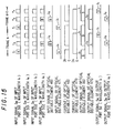
- the optical bistable elements 461 and 470 are respectively supplied with the currents i each decreases periodically as shown in Fig. 15, so that the optical bistable elements 461 and 470 become at a reset state periodically in different timings. Therefore, the optical bistable elements 461 and 470 respectively keep supplying the output signal B of wavelengths ⁇ 1 and the output signal A of wavelength ⁇ 2 to the optical read switches 481 and 484 for the period until the current i decreases.
- the optical read switch 481 supplies the output signal of wavelength ⁇ 1 in the time slot T 3 to the optical combiner 491 and the optical read switch 484 supplies the output signal of wavelength ⁇ 2 in the time slot T 2 to the optical combiner 492. Consequently, an output signal S 41 including a signal of wavelength ⁇ 1 in the time slot T 3 is supplied from the output port 511, while an output signal S 51 including a signal of wavelength ⁇ 2 in the time slot T 2 is supplied from the output port 512.
Landscapes
- Engineering & Computer Science (AREA)
- Computer Networks & Wireless Communication (AREA)
- Use Of Switch Circuits For Exchanges And Methods Of Control Of Multiplex Exchanges (AREA)
- Optical Communication System (AREA)
Applications Claiming Priority (5)
| Application Number | Priority Date | Filing Date | Title |
|---|---|---|---|
| JP43020/91 | 1991-02-14 | ||
| JP3043020A JPH04260295A (ja) | 1991-02-14 | 1991-02-14 | 波長分割・時分割複合光交換機 |
| JP3044432A JPH04262697A (ja) | 1991-02-15 | 1991-02-15 | 波長分割・時分割複合光通話路 |
| JP44432/91 | 1991-02-15 | ||
| EP19920102417 EP0499255A3 (en) | 1991-02-14 | 1992-02-13 | Optical switching system for optical wavelength-division and time-division multiplexed signals |
Related Parent Applications (2)
| Application Number | Title | Priority Date | Filing Date |
|---|---|---|---|
| EP19920102417 Division EP0499255A3 (en) | 1991-02-14 | 1992-02-13 | Optical switching system for optical wavelength-division and time-division multiplexed signals |
| EP92102417.0 Division | 1992-02-13 |
Publications (2)
| Publication Number | Publication Date |
|---|---|
| EP0765097A2 true EP0765097A2 (de) | 1997-03-26 |
| EP0765097A3 EP0765097A3 (de) | 1998-12-02 |
Family
ID=26382764
Family Applications (2)
| Application Number | Title | Priority Date | Filing Date |
|---|---|---|---|
| EP19920102417 Withdrawn EP0499255A3 (en) | 1991-02-14 | 1992-02-13 | Optical switching system for optical wavelength-division and time-division multiplexed signals |
| EP96117346A Withdrawn EP0765097A3 (de) | 1991-02-14 | 1992-02-13 | Optisches Vermittlungssystem für optische Wellenlängen- und Zeitmultiplexsignale |
Family Applications Before (1)
| Application Number | Title | Priority Date | Filing Date |
|---|---|---|---|
| EP19920102417 Withdrawn EP0499255A3 (en) | 1991-02-14 | 1992-02-13 | Optical switching system for optical wavelength-division and time-division multiplexed signals |
Country Status (3)
| Country | Link |
|---|---|
| US (1) | US5404240A (de) |
| EP (2) | EP0499255A3 (de) |
| CA (1) | CA2061141C (de) |
Cited By (1)
| Publication number | Priority date | Publication date | Assignee | Title |
|---|---|---|---|---|
| EP1126739A1 (de) * | 2000-02-15 | 2001-08-22 | Lucent Technologies Inc. | Verfahren und Vorrichtung zur Speicherung Digitaler Optischer Signale |
Families Citing this family (23)
| Publication number | Priority date | Publication date | Assignee | Title |
|---|---|---|---|---|
| FR2715015B1 (fr) * | 1994-01-07 | 1996-02-02 | Auffret Rene | Procédé et dispositif de transmission et d'aiguillage de paquets dans un réseau optique. |
| US5446809A (en) * | 1994-09-23 | 1995-08-29 | United Technologies Corporation | All fiber wavelength selective optical switch |
| US5949562A (en) * | 1994-11-30 | 1999-09-07 | Canon Kabushiki Kaisha | Transmission wavelength control method permitting efficient wavelength multiplexing, optical communication method, optical transmitter, optical transmitter-receiver apparatus, and optical communication system |
| JP3060994B2 (ja) * | 1997-05-15 | 2000-07-10 | 日本電気株式会社 | N−wdmシステムにおける出力ポート切替装置 |
| US5885943A (en) * | 1997-12-18 | 1999-03-23 | Exxon Chemical Patents Inc. | Sulfur boron antiwear agents for lubricating compositions |
| US6058227A (en) * | 1998-01-29 | 2000-05-02 | Trw Inc. | Method and apparatus for an opto-electronic circuit switch |
| US7386236B1 (en) | 1999-09-27 | 2008-06-10 | Alloptic, Inc. | Multiple wavelength TDMA optical network |
| US6944406B1 (en) * | 2000-08-04 | 2005-09-13 | Fujitsu Limited | Transport system with tunable channel spacing DWDM |
| US20020155196A1 (en) * | 2000-08-18 | 2002-10-24 | Kiely Alice Mary O. | Edible cookie supports for comestibles with optional, edible mess guards and drip guards |
| TW575747B (en) * | 2002-06-07 | 2004-02-11 | Delta Electronics Inc | Waveband-selective optical switch |
| US20040160596A1 (en) * | 2003-02-19 | 2004-08-19 | Pactonix, Inc. | Apparatus and method to accurately monitor signal quality in optical signal transmission systems |
| CN1745530B (zh) * | 2003-11-20 | 2012-10-03 | 日本电信电话株式会社 | 波分复用传送系统 |
| US7903973B1 (en) | 2005-12-23 | 2011-03-08 | Lockheed Martin Corporation | Dynamic temporal duration optical transmission privacy |
| US7792427B1 (en) | 2006-01-30 | 2010-09-07 | Lockheed Martin Corporation | Optical code division multiple access data storage and retrieval |
| US7991288B1 (en) * | 2006-02-07 | 2011-08-02 | Lockheed Martin Corporation | Optical code division multiple access data storage encryption and retrieval |
| EP2347483B1 (de) | 2008-11-04 | 2017-07-19 | Massachusetts Institute of Technology | Eindimensionales mehrfachwellenlängen-strahlkombinieren mit externem resonator von zweidimensionalen laserelementen |
| US8614853B2 (en) | 2010-03-09 | 2013-12-24 | Massachusetts Institute Of Technology | Two-dimensional wavelength-beam-combining of lasers using first-order grating stack |
| US8531761B2 (en) | 2010-05-27 | 2013-09-10 | Massachusetts Institute Of Technology | High peak power optical amplifier |
| US9620928B2 (en) | 2010-07-16 | 2017-04-11 | Massachusetts Institute Of Technology | Continuous wave or ultrafast lasers |
| US9712899B2 (en) * | 2014-12-11 | 2017-07-18 | Alcatel Lucent | Hybrid optical switch for software-defined networking |
| US9703048B2 (en) * | 2015-07-07 | 2017-07-11 | Huawei Technologies Co., Ltd. | Apparatus and method for tuning optical components |
| US9766403B2 (en) | 2015-07-07 | 2017-09-19 | Huawei Technologies Co., Ltd. | Apparatus and method for tuning and switching between optical components |
| JP7106016B2 (ja) * | 2019-11-18 | 2022-07-25 | 三菱電機株式会社 | 光通信システムおよび光通信方法 |
Family Cites Families (8)
| Publication number | Priority date | Publication date | Assignee | Title |
|---|---|---|---|---|
| JPS62206996A (ja) * | 1986-03-07 | 1987-09-11 | Hitachi Ltd | 光交換方法およびその装置 |
| JPH0754988B2 (ja) * | 1986-07-23 | 1995-06-07 | 富士通株式会社 | 波長分割型光交換通話路 |
| JPH0714228B2 (ja) * | 1986-08-20 | 1995-02-15 | 富士通株式会社 | 時分割波長分割併合型光交換通話路装置 |
| JPS6490696A (en) * | 1987-09-30 | 1989-04-07 | Nec Corp | Wavelength/time division optical exchange |
| EP0642288B1 (de) * | 1987-09-30 | 2002-06-12 | NEC Corporation | Zeit- und Wellenlängenmultiplex-Umschaltsystem |
| JPH0267525A (ja) * | 1988-09-02 | 1990-03-07 | Hitachi Ltd | 光スイツチ装置及びスイツチ間伝送方法 |
| JP2692316B2 (ja) * | 1989-11-20 | 1997-12-17 | 日本電気株式会社 | 波長分割光交換機 |
| FR2665039B1 (fr) * | 1990-07-17 | 1994-03-25 | France Telecom | Systeme de commutation optique de signaux multiplexes en frequence. |
-
1992
- 1992-02-13 CA CA002061141A patent/CA2061141C/en not_active Expired - Lifetime
- 1992-02-13 EP EP19920102417 patent/EP0499255A3/en not_active Withdrawn
- 1992-02-13 EP EP96117346A patent/EP0765097A3/de not_active Withdrawn
- 1992-02-14 US US07/835,304 patent/US5404240A/en not_active Expired - Lifetime
Non-Patent Citations (1)
| Title |
|---|
| ELECTRONICS LETTERS, vol. 23, no. 20, 24 September 1987 (1987-09-24), pages 1088 - 1089 |
Cited By (1)
| Publication number | Priority date | Publication date | Assignee | Title |
|---|---|---|---|---|
| EP1126739A1 (de) * | 2000-02-15 | 2001-08-22 | Lucent Technologies Inc. | Verfahren und Vorrichtung zur Speicherung Digitaler Optischer Signale |
Also Published As
| Publication number | Publication date |
|---|---|
| EP0499255A2 (de) | 1992-08-19 |
| US5404240A (en) | 1995-04-04 |
| CA2061141A1 (en) | 1992-08-15 |
| CA2061141C (en) | 1996-09-10 |
| EP0499255A3 (en) | 1993-11-10 |
| EP0765097A3 (de) | 1998-12-02 |
Similar Documents
| Publication | Publication Date | Title |
|---|---|---|
| US5404240A (en) | Optical switching system for optical wavelength-division and time-division multiplexed signals | |
| Zhong et al. | Wavelength routing-based photonic packet buffers and their applications in photonic packet switching systems | |
| Dorren et al. | Optical packet switching and buffering by using all-optical signal processing methods | |
| DE69529626T2 (de) | Optischer wellenleiterkreuzungspunktschalter | |
| CA1331800C (en) | Time and wavelength division switching system | |
| US6069720A (en) | Optical telecommunications network | |
| KR0142177B1 (ko) | 광 스위치 및 그 스위칭 모듈 | |
| US4754132A (en) | Symmetric optical device with quantum well absorption | |
| DE69431463T2 (de) | Optischer FIFO Puffer mit Frequenzmultiplexierung | |
| CA1206633A (en) | Optical time-division switching system employing optical bistable devices | |
| EP0347903A3 (de) | Schnelles optisches Paketvermittlungssystem mit optischen Puffern zwischen ankommenden und abgehenden Kanälen | |
| EP0923264B1 (de) | Optische Koppelmatrix für Wellenlängen- Multiplexsignale | |
| US5103333A (en) | Photonic time-slot interchangers using cascade-structured integrated optical switches | |
| US4923267A (en) | Optical fiber shift register | |
| US5375004A (en) | Light connecting device and method of driving the same | |
| US5058060A (en) | Optical memory cell | |
| Hinton | Photonics in switching | |
| JPS60254991A (ja) | 時分割光交換機 | |
| Ito et al. | Extremely low power consumption semiconductor optical amplifier gate for WDM applications | |
| JP2737926B2 (ja) | 光スイッチ装置 | |
| JP2527553B2 (ja) | 光多元交換装置 | |
| CA2253485C (en) | Optical clock division | |
| KR100368899B1 (ko) | 3단스위칭유닛 | |
| Papadimitriou et al. | OCON: an optically controlled optical network | |
| US6542269B1 (en) | Optical device for processing an optical impulse |
Legal Events
| Date | Code | Title | Description |
|---|---|---|---|
| PUAI | Public reference made under article 153(3) epc to a published international application that has entered the european phase |
Free format text: ORIGINAL CODE: 0009012 |
|
| AC | Divisional application: reference to earlier application |
Ref document number: 499255 Country of ref document: EP |
|
| AK | Designated contracting states |
Kind code of ref document: A2 Designated state(s): DE FR GB NL SE |
|
| PUAL | Search report despatched |
Free format text: ORIGINAL CODE: 0009013 |
|
| AK | Designated contracting states |
Kind code of ref document: A3 Designated state(s): DE FR GB NL SE |
|
| 17P | Request for examination filed |
Effective date: 19981104 |
|
| 17Q | First examination report despatched |
Effective date: 20000214 |
|
| STAA | Information on the status of an ep patent application or granted ep patent |
Free format text: STATUS: THE APPLICATION IS DEEMED TO BE WITHDRAWN |
|
| 18D | Application deemed to be withdrawn |
Effective date: 20000825 |