EP0769810A2 - Bipolarer Transistor und Verfahren zu dessen Herstellung - Google Patents
Bipolarer Transistor und Verfahren zu dessen Herstellung Download PDFInfo
- Publication number
- EP0769810A2 EP0769810A2 EP96116180A EP96116180A EP0769810A2 EP 0769810 A2 EP0769810 A2 EP 0769810A2 EP 96116180 A EP96116180 A EP 96116180A EP 96116180 A EP96116180 A EP 96116180A EP 0769810 A2 EP0769810 A2 EP 0769810A2
- Authority
- EP
- European Patent Office
- Prior art keywords
- layer
- conductivity type
- semiconductor substrate
- molecular beam
- beam epitaxy
- Prior art date
- Legal status (The legal status is an assumption and is not a legal conclusion. Google has not performed a legal analysis and makes no representation as to the accuracy of the status listed.)
- Withdrawn
Links
Images


Classifications
-
- H—ELECTRICITY
- H10—SEMICONDUCTOR DEVICES; ELECTRIC SOLID-STATE DEVICES NOT OTHERWISE PROVIDED FOR
- H10P—GENERIC PROCESSES OR APPARATUS FOR THE MANUFACTURE OR TREATMENT OF DEVICES COVERED BY CLASS H10
- H10P30/00—Ion implantation into wafers, substrates or parts of devices
- H10P30/20—Ion implantation into wafers, substrates or parts of devices into semiconductor materials, e.g. for doping
- H10P30/21—Ion implantation into wafers, substrates or parts of devices into semiconductor materials, e.g. for doping of electrically active species
-
- H—ELECTRICITY
- H10—SEMICONDUCTOR DEVICES; ELECTRIC SOLID-STATE DEVICES NOT OTHERWISE PROVIDED FOR
- H10D—INORGANIC ELECTRIC SEMICONDUCTOR DEVICES
- H10D10/00—Bipolar junction transistors [BJT]
- H10D10/01—Manufacture or treatment
- H10D10/051—Manufacture or treatment of vertical BJTs
- H10D10/054—Forming extrinsic base regions on silicon substrate after insulating device isolation in vertical BJTs having single crystalline emitter, collector or base regions
-
- H—ELECTRICITY
- H10—SEMICONDUCTOR DEVICES; ELECTRIC SOLID-STATE DEVICES NOT OTHERWISE PROVIDED FOR
- H10P—GENERIC PROCESSES OR APPARATUS FOR THE MANUFACTURE OR TREATMENT OF DEVICES COVERED BY CLASS H10
- H10P30/00—Ion implantation into wafers, substrates or parts of devices
- H10P30/20—Ion implantation into wafers, substrates or parts of devices into semiconductor materials, e.g. for doping
- H10P30/202—Ion implantation into wafers, substrates or parts of devices into semiconductor materials, e.g. for doping characterised by the semiconductor materials
- H10P30/204—Ion implantation into wafers, substrates or parts of devices into semiconductor materials, e.g. for doping characterised by the semiconductor materials into Group IV semiconductors
Definitions
- the invention relates to a semiconductor device and a method of fabricating the same, and more particularly to a semiconductor device having layers formed by means of molecular beam epitaxy and a method of fabricating a semiconductor device by using an apparatus for carrying out molecular beam epitaxy.
- Japanese Unexamined Patent Publication No. 5-211158 has suggested a method of fabricating a semiconductor device by means of molecular beam epitaxy (hereinafter, referred to simply as "MBE"). Hereinbelow is explained the method with reference to Figs. 1A to 1D.
- MBE molecular beam epitaxy
- an N - epitaxial layer 2 over an N-type silicon substrate 1.
- the N - epitaxial layer 2 has a thickness ranging from 0.8 to 1.3 ⁇ m, and a resistivity ranging from 0.5 to 1.0 ⁇ -cm.
- the N - epitaxial layer 2 is thermally oxidized to thereby form a silicon dioxide film 3 having a thickness of about 100 nm.
- a part of the silicon dioxide film 3 is removed by photolithography and anisotropic etching to thereby form a base region.
- MBE apparatus an apparatus for carrying out molecular beam epitaxy
- MBE apparatus which provides about 10 -8 Torr vacuum to thereby form a P-type layer 4 on the N - epitaxial layer 2 at 650 °C of growth temperature.
- the P-type layer 4 has a thickness in the range of 30 to 50 nm, and a carrier concentration on the order of 10 18 cm -3 .
- an MBE layer an layer formed by means of the MBE apparatus, including the P-type layer 4
- silicon and boron are evaporated again in the MBE apparatus to thereby form a P - MBE layer 5 over the P-type MBE layer 4 at 650 °C of growth temperature.
- the P - MBE layer 5 has a thickness in the range of 5 to 20 nm.
- the P - MBE layer 5 functions as a buffer layer for maintaining both crystallinity at an interface between an emitter and a base and p-n junction in well condition.
- polysilicon having grown on the silicon dioxide film 3 are removed by means of photolithography and anisotropic etching such as CF 4 gas etching.
- a silicon dioxide film 6 and further a silicon nitride film 7 are formed on the P - MBE layer 5 and the silicon dioxide film 3 by chemical vapor deposition (CVD).
- the silicon dioxide film 6 and the silicon nitride film 7 both have a thickness of about 100 nm.
- a photoresist 8 is deposited over the silicon nitride film 7, and patterned by photolithography, followed by anisotropic etching to thereby open an emitter region E.
- silicon and antimony are evaporated in the MBE apparatus to thereby deposit heavily doped amorphous silicon on the silicon substrate 1 at room temperature, followed by solid phase epitaxy at growth temperature of 730 °C to thereby form an N + MBE layer 9 having a thickness in the range of 100 to 200 nm.
- photolithography and subsequently anisotropic etching such as (CF 4 +O 2 ) gas etching are carried out to the N + MBE layer 9 to thereby form an emitter contact 9a.
- the thus obtained emitter contact 9a composed of the N + MBE layer 9 has been already sufficiently activated. Thus, it is no longer necessary to carry out thermal annealing at high temperature above growth temperature, resulting in that impurities depth profile is scarcely varied, and that it is possible to obtain desired characteristics by controlling thickness of base and emitter and/or carrier concentration.
- the photoresist 8 is patterned by photolithography and anisotropically etched to thereby open a base contact B.
- a titanium (Ti)/platinum (Pt) layer 10 is deposited all over a resultant by vacuum evaporation.
- a gold layer 11 is deposited on the Ti/Pt layer 10, and then patterned by photolithography.
- the Ti/Pt layer 10 is anisotropically etched using the patterned gold layer 11 as a mask, to thereby form electrodes of base and emitter of a silicon bipolar transistor.
- the above mentioned conventional method has an advantage that an emitter region almost free of crystal defects can be obtained without carrying out thermal annealing at high temperature for activation, because the thin base layer 4 is grown by MBE, and further the N + MBE layer 9 is grown through solid phase epitaxy process by means of the MBE apparatus. To the contrary, the above mentioned conventional method has many shortcomings.
- the emitter region is insufficiently shallow in depth, because the emitter region is established only through annealing in solid phase epitaxy.
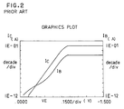
- Fig. 2 shows Gummel plots for a transistor fabricated in accordance with the above mentioned conventional method. It is understood in view of the two curves I C and I B in Fig. 2 that a base current IB is greater than a collector current Ic in the range where a current is small, resulting in that the forward current gain linearity is deteriorated.
- a rapid thermal annealing (RTA) apparatus may be used in the conventional method to carry out implantation for forming a shallow emitter region.
- RTA rapid thermal annealing
- annealing is carried out in so short period of time that temperature in a wafer is not uniformized. As a result, there is generated dispersion in characteristics, which lowers a production yield.
- Ion implantation and thermal diffusion which have been widely used, have a shortcoming that they make the implantation depth so deep that crystal defects are increased, resulting in that it is necessary to carry out thermal annealing at high temperature for activation.
- those prior methods have another shortcoming that a silicon wafer has to be taken out of an MBE apparatus each time when ion implantation is to be carried out.
- a method of fabricating a semiconductor device comprising the steps of: (a) forming a first molecular beam epitaxy layer on a semiconductor substrate; and (b) forming a second molecular beam epitaxy layer on the first molecular beam epitaxy layer, characterized by the step of: (c) implanting impurities into the first molecular beam epitaxy layer prior to the step (b).
- the method further include the steps of: (d) forming a heavily doped first conductivity type layer buried in the semiconductor substrate, the semiconductor substrate having a second conductivity type; (e) forming a lightly doped first conductivity type epitaxial layer on the heavily doped first conductivity type layer so that the lightly doped first conductivity type epitaxial layer is exposed to a surface of the semiconductor substrate; and (f) forming a heavily doped first conductivity type connection layer for connecting the heavily doped first conductivity type layer to a surface of the semiconductor substrate.
- the steps (d), (e) and (f) are to be carried out in sequence prior to the step (a).
- the first molecular beam epitaxy layer is formed on the lightly doped first conductivity type epitaxial layer.
- the second molecular beam epitaxy layer is formed on both the connection layer and a part of the first molecular beam epitaxy layer into which the impurities are implanted.
- the second molecular beam epitaxy layer is designed to be of a first conductivity type.
- the second molecular beam epitaxy layer is formed only on a portion of the first molecular beam epitaxy layer into which the impurities have been implanted.
- the first molecular beam epitaxy layer may be designed to have an opposite conductivity to that of the semiconductor substrate, and the second molecular beam epitaxy layer may have the same conductivity as that of the semiconductor substrate.
- the first molecular beam epitaxy layer may be comprised of a first epitaxial layer and the second molecular beam epitaxy layer may be comprised of an amorphous layer.
- the method may further include the step of causing the second molecular beam epitaxy layer to grow in solid phase to a second epitaxial layer and a polysilicon layer.
- a method of fabricating a semiconductor device comprising the steps of: (a) forming a first conductivity type epitaxial layer on a second conductivity type semiconductor substrate; and (b) forming a second conductivity type layer on the first conductivity type epitaxial layer, characterized by the steps of: (c) implanting second conductivity type impurities into at least a part of the first conductivity type epitaxial layer, the second conductivity type layer being formed on the part of the first conductivity type epitaxial layer into which the second conductivity type impurities have been implanted; and (d) causing the second conductivity type layer to grow in solid phase, the second conductivity type layer being an amorphous layer.
- the method further include the steps of: (e) forming a heavily doped second conductivity type layer buried in the semiconductor substrate; (f) forming a lightly doped second conductivity type epitaxial layer on the heavily doped second conductivity type layer so that the lightly doped second conductivity type epitaxial layer is exposed to a surface of the semiconductor substrate; (g) forming a heavily doped second conductivity type connection layer for connecting the heavily doped second conductivity type layer to a surface of the semiconductor substrate.
- the steps (e), (f) and (g) are to be carried out in sequence prior to the step (a).
- a method of fabricating a semiconductor device comprising the steps of: (a) forming a first conductivity type base region in a second conductivity type collector region by molecular beam epitaxy; and (b) forming a second conductivity type layer on the first conductivity type base region by molecular beam epitaxy, characterized by the steps of: (c) forming an emitter region in the base region by implanting second conductivity type impurities into the base region by molecular beam epitaxy, the second conductivity type layer being formed on the emitter region, the second conductivity type layer being formed of an amorphous layer; and (d) forming an emitter contact region by causing the second conductivity type amorphous layer to grow in solid phase.
- the method further include (e) forming a heavily doped second conductivity type layer buried in a first conductivity type semiconductor substrate; (f) forming a lightly doped second conductivity type epitaxial layer on the heavily doped second conductivity type layer so that the lightly doped second conductivity type epitaxial layer is exposed to a surface of the semiconductor substrate; and (g) forming a heavily doped second conductivity type connection layer for connecting the heavily doped second conductivity type layer to a surface of the semiconductor substrate.
- the steps (e), (f) and (g) are to be carried out in sequence prior to the step (a).
- the second conductivity type layer is formed also on the connection layer.
- the steps where molecular beam epitaxy is to be accomplished may be carried out in a common apparatus for accomplishing molecular beam epitaxy.
- the impurities are selected from antimony (Sb), phosphorus (P) and arsenic (As). Impurities implantation is accomplished by application of a voltage directly to the semiconductor substrate during doping.
- a semiconductor device comprising: (a) a first conductivity type semiconductor substrate; (b) a first molecular beam epitaxy layer formed on the semiconductor substrate, the first molecular beam epitaxy layer being of a second conductivity type; and (c) a second molecular beam epitaxy layer formed on the impurities implantation layer, the second molecular beam epitaxy layer being of a first conductivity type, characterized by the step of: (d) an impurities implantation layer into which first conductivity type impurities are implanted, formed at a surface of the first molecular beam epitaxy layer.
- the semiconductor device prefferably includes (e) a heavily doped first conductivity type layer buried in the semiconductor substrate; (f) a lightly doped first conductivity type epitaxial layer formed on the heavily doped first conductivity type layer so that the lightly doped first conductivity type epitaxial layer is exposed to a surface of the semiconductor substrate; and (g) a heavily doped first conductivity type connection layer for connecting the heavily doped first conductivity type layer to a surface of the semiconductor substrate.
- the second molecular beam epitaxy layer is formed also on the connection layer.
- the first molecular beam epitaxy layer may be comprised of an epitaxial layer, and the second molecular beam epitaxy layer may be comprised of an amorphous layer.
- the impurities are selected from antimony (Sb), phosphorus (Pb) and arsenic (As).
- a semiconductor device comprising: (a) a first conductivity type semiconductor substrate; (b) a second conductivity type epitaxial layer formed on the semiconductor substrate; and (c) a first conductivity type layer formed on the second conductivity type epitaxial layer, characterized by: (d) an impurities implantation layer comprised of a part of the second conductivity type epitaxial layer into which first conductivity type impurities are implanted.
- the first conductivity type layer is formed on the impurities implantation layer, and is comprised of an amorphous layer.
- the semiconductor device prefferably includes: (e) a heavily doped first conductivity type layer buried in the semiconductor substrate; (f) a lightly doped first conductivity type epitaxial layer formed on the heavily doped first conductivity type layer so that the lightly doped first conductivity type epitaxial layer is exposed to a surface of the semiconductor substrate; and (g) a heavily doped first conductivity type connection layer for connecting the heavily doped first conductivity type layer to a surface of the semiconductor substrate.
- the first conductivity type layer is formed also on the connection layer, and is comprised of an amorphous layer.
- a semiconductor device comprising: (a) a first conductivity type semiconductor substrate; (b) a second conductivity type base region formed in a first conductivity type collector region of the semiconductor substrate; and (c) a first conductivity type layer formed on the emitter region, characterized by: (d) an emitter region formed in the base region, first conductivity type impurities being implanted into the emitter region.
- the semiconductor device prefferably includes: (e) a heavily doped first conductivity type layer buried in the semiconductor substrate; (f) a lightly doped first conductivity type epitaxial layer formed on the heavily doped first conductivity type layer so that the lightly doped first conductivity type epitaxial layer is exposed to a surface of the semiconductor substrate; and (g) a heavily doped first conductivity type connection layer for connecting the heavily doped first conductivity type layer to a surface of the semiconductor substrate.
- the first conductivity type layer is formed also on the connection layer, and is comprised of an amorphous layer.
- the emitter region can have a shallow depth and a uniform, sufficient impurities content by implanting impurities such as antimony (Sb) into a region with a substrate being DC-biased in an MBE apparatus.
- impurities such as antimony (Sb)
- Sb antimony
- a p-n junction interfacial plane is formed in a base epitaxial layer, it is possible to obtain better crystallinity with the result of improvement in DC characteristic.
- Figs. 1A to 1D are cross-sectional views of a silicon bipolar transistor, each illustrating respective step of a conventional method of fabricating a silicon bipolar transistor.
- Fig. 2 shows Gummel plots for a conventional silicon bipolar transistor.
- Fig. 3 is a cross-sectional view of a silicon bipolar transistor fabricated in accordance with the first embodiment of the present invention.
- Figs. 4A to 4G are cross-sectional views of a silicon bipolar transistor fabricated in accordance with the first embodiment of the present invention, each illustrating respective step of a method of fabricating the same.
- Fig. 5 shows Gummel plots for a silicon bipolar transistor fabricated in accordance with the first embodiment of the present invention.
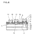
- Fig. 6 is a cross-sectional view of a silicon bipolar transistor fabricated in accordance with the second embodiment of the present invention.
- Figs. 7A to 7D are cross-sectional views of a silicon bipolar transistor fabricated in accordance with the second embodiment of the present invention, each illustrating respective step of a method of fabricating the same.
- Fig. 3 is a cross-sectional view of a silicon bipolar transistor fabricated in accordance with the first embodiment of the present invention.
- the illustrated silicon bipolar transistor includes a N-type silicon substrate 1 in which an N - epitaxial layer 2 is formed. On the N - epitaxial layer 2 are formed silicon dioxide films 3 between which a device formation region is formed. On the N - epitaxial layer 2 and between the silicon dioxide films 3 is deposited a P-type MBE layer formed by means of molecular beam epitaxy. Impurities such as antimony (Sb) are implanted into a part of the P-type MBE layer 4 to thereby form an impurities implantation layer 12 at a surface of the P-type MBE layer 4.
- Sb antimony
- a silicon dioxide film 6 and a silicon nitride film 7 are deposited on the N - epitaxial layer 2 and the silicon dioxide films 3 to thereby form two openings, one of which forms an emitter region in alignment with the impurities implantation layer 12, and the other forms a base region.
- an N + MBE layer 9 is deposited on the impurities implantation layer 12 by molecular beam epitaxy to thereby form an emitter contact 9a.
- the N - epitaxial layer 2 has a thickness ranging from 0.8 to 1.3 ⁇ m, and a resistivity ranging from 0.5 to 1.0 ⁇ -cm.
- the N - epitaxial layer 2 is thermally oxidized to thereby form a silicon dioxide film 3 having a thickness of about 100 nm.
- a part of the silicon dioxide film 3 is removed by photolithography and anisotropic etching to thereby form a base region.
- silicon and boron are evaporated in an MBE apparatus which provides about 10 -8 Torr vacuum, to thereby form a P-type layer 4 on the N - epitaxial layer 2 at 650 °C of growth temperature.
- the P-type layer 4 has a thickness in the range of 30 to 50 nm, and a carrier concentration on the order of 10 18 cm -3 .
- the P - MBE layer may have a thickness in the range of 5 to 20 nm.
- the growth temperature is determined in dependence on plane azimuth of a substrate. In general, the growth is continued for a couple of minutes at temperature in the range of 620 °C to 700 °C.
- polysilicon having grown on the silicon dioxide films 3 are removed by means of photolithography and anisotropic etching such as CF 4 gas etching.
- a silicon dioxide film 6 and further a silicon nitride film 7 are formed on the P-type MBE layer 5 and the silicon dioxide films 3 by chemical vapor deposition (CVD).
- the silicon dioxide film 6 and the silicon nitride film 7 both have a thickness of about 100 nm.
- a photoresist 8 is deposited over the silicon nitride film 7, and patterned by photolithography, followed by anisotropic etching to thereby open an emitter region E.
- antimony (Sb) ions are implanted to a resultant from knudsen cells equipped with the MBE apparatus, as illustrated in Fig. 4C.
- Sb ions implantation a voltage is applied to the silicon substrate 1 in the range of -1 to -3 kV in the MBE apparatus.
- the DC bias facilitates ionized Sb atoms to be implanted into the P-type MBE layer 4, resulting in that a shallow N + Sb implantation layer 12 is formed in the P-type MBE layer 4.
- the Sb atoms are implanted into the P-type MBE layer 4 at a dose of 1 ⁇ 10 19 to 10 20 atoms/cm 3 at a depth in the range of 5 to 20 nm.
- phosphorus (P) or arsenic (As) atoms may be implanted into the P-type MBE layer 4.
- P phosphorus
- arsenic arsenic
- atoms having a heavy atomic weight such as P and As have a shortcoming that they are likely to be implanted too deep.
- antimony atoms have a small atomic weight, it is possible to control them so that they are implanted into the P-type MBE layer 4 at a shallow depth. Thus, it is most preferable to use antimony as impurities.
- An implantation depth of antimony atoms is about tens of nanometers at greatest, which cannot be accomplished by usual ion implantation.
- the term "MBE apparatus” indicates an apparatus for forming a thin film by epitaxial growth, in particular, gas phase epitaxy, in further particular, physical deposition.
- MBE apparatus composition elements are transformed into molecular beam in the form of beam under ultra-high vacuum, and then the beam is irradiated to a substrate to thereby carry out epitaxy.
- the growth rate is so small that it is relatively easy to form a thin film. It is also possible to form an epitaxial layer having good crystallinity by thermal treatment at low temperature.
- ionized atoms exist in the molecular beam in the MBE apparatus. These ionized atoms are implanted into the silicon substrate at a shallow depth by directly DC-biasing the silicon substrate in the MBE apparatus. This process gives little damage to the substrate, and makes it possible to activate those ionized atoms with thermal treatment even at low temperature.
- heavily doped amorphous silicon is deposited on the silicon nitride film 7 and the Sb implantation layer 12 at room temperature by evaporating silicon and antimony in the MBE apparatus, followed by carrying out solid phase epitaxy process at growth temperature of 730 °C to thereby form an N + MBE layer 9 having a thickness in the range of 100 to 200 nm.
- the Sb implantation layer 12 is activated simultaneously with the formation of the N + MBE layer 9 to thereby establish an emitter region E.
- the conditions for growth of the N + MBE layer 9 are follows.
- a layer formed by solid phase epitaxy process can have less crystal defects than a layer formed by other processes. Since there are much generated crystal defects in a layer formed by widely used usual ion implantation process, it is necessary to thermally treat the layer at high temperature for activation in the usual ion implantation. On the other hand, the ion implantation to be carried out with a silicon substrate being DC-biased in the MBE apparatus needs less energy for implantation than the usual ion implantation. Thus, the silicon substrate is less damaged, and hence can be sufficiently activated even at low temperature, resulting in that it is no longer necessary in the embodiment to thermally treat the substrate at high temperature. In addition, since it is possible to carry out a series of fabrication steps in an MBE apparatus, time and cost for fabrication can be significantly saved.
- a photoresist 8 is deposited over the N + MBE layer 9 and patterned by photolithography, and then etched by anisotropic etching such as (CF 4 +O 2 ) gas etching to thereby form an emitter contact 9a.
- anisotropic etching such as (CF 4 +O 2 ) gas etching.
- a photoresist 8 is deposited again over a resultant, and patterned by photolithography. Then, as illustrated in Fig. 4F, the photoresist 8 is anisotropically etched to thereby open a base contact B.
- a titanium (Ti)/platinum (Pt) layer 10 is deposited all over a resultant by vacuum evaporation.
- a gold layer 11 is deposited on the Ti/Pt layer 10, and then patterned by lithography.
- the Ti/Pt layer 10 is anisotropically etched using the patterned gold layer 11 as a mask, to thereby form electrodes of base and emitter of the silicon bipolar transistor.
- a base but also an emitter are grown in an MBE apparatus, and impurities such as antimony (Sb) are implanted into a substrate at a shallow depth with the substrate being DC-biased in the MBE apparatus.
- impurities such as antimony (Sb) are implanted into a substrate at a shallow depth with the substrate being DC-biased in the MBE apparatus.
- a p-n junction interfacial plane is formed in a base epitaxial layer, and hence, it is possible to form an emitter region having a shallow depth and sufficient impurities concentration with the result of prevention of deterioration of DC characteristic.
- epitaxial phase and polysilicon phase are not uniform in the vicinity of an interface between them in an emitter region due to solid phase diffusion, but a uniform p-n junction interface can be formed in a base epitaxial layer.
- Fig. 5 shows Gummel plots for a transistor fabricated in accordance with the above mentioned embodiment. It is understood in view of Fig. 5 that a base current I B is smaller than conventional one shown in Fig. 2 at a low current region (axis of ordinate). As a result, it is understood that the forward current gain linearity is improved.
- germanium (Ge) is evaporated from another knudsen cell in the MBE apparatus at an appropriate growth rate together with silicon and boron when the P + MBE layer 4 is to be formed, it makes a SiGe heterojunction-bipolar transistor.
- Fig. 6 illustrates an integrated circuit including a silicon bipolar transistor fabricated in accordance with the second embodiment of the present invention.
- the illustrated silicon bipolar transistor includes a P-type silicon substrate 21 in which there is formed an N + buried layer 22.
- the N + buried layer 22 is formed by implanting impurities such as arsenic (As) and antimony (Sb) into the P-type silicon substrate 21.
- an N - epitaxial layer 2 having a thickness ranging from 0.8 to 1.3 ⁇ m and resistivity ranging from 0.5 to 1.0 ⁇ cm.
- the collector electrode As illustrated in Fig. 6 at the left half, on the N - epitaxial layer 2 are formed base and emitter electrodes which are the same as those of the first embodiment described with reference to in Figs. 3 and 4A to 4G.
- a collector electrode On the N + connection layer 23 is formed a collector electrode having the same structure as that of the emitter electrode. Namely, the collector electrode includes the N + MBE layer 9 formed directly on the N + connection layer 23, the Ti/Pt layer 10 formed on the N + MBE layer 9, and the gold layer 11 formed on the Ti/Pt layer 10.
- a photoresist (not illustrated) is deposited all over the P-type silicon substrate 21, and then patterned by photolithography and anisotropic etching so that the photoresist does not exist on a region where the N + buried layer 22 is to be formed. Then, as illustrated in Fig. 7A, impurities such as arsenic (As) are implanted into the P-type silicon substrate 21 to thereby form the N + buried layer 22.
- the N - epitaxial layer 2 is epitaxially grown on the N + buried layer 22 by chemical vapor deposition.
- a photoresist 25 is deposited over the silicon substrate 21 and patterned so that a collector region is open. Thereafter, impurities such as phosphorus (P) is implanted into the silicon substrate 21.
- the N + connection layer 23 is formed extending through the N - epitaxial layer 2 for connecting the N + buried layer 22 to a later formed collector electrode.
- the base and emitter electrodes are formed in the same manner as the first embodiment described with reference to Figs. 4A to 4G.
- a collector electrode is also formed on the N + connection layer 23 in the same manner as the emitter electrode.
- the silicon bipolar transistor fabricated in accordance with the present invention is applicable to various integrated circuits such as Bi-CMOS.
- the second embodiment it is possible also in the second embodiment to fabricate an integrated circuit including a SiGe heterojunction-bipolar transistor by evaporating germanium at an appropriate growth rate together with silicon and boron when the P + MBE layer 4 is formed in the MBE apparatus.
- the application of the present invention is not to be limited to a bipolar transistor.
- the present invention can be applied to a thyrister and other semiconductor devices. It is possible to use a semiconductor substrate other than a silicon substrate.
- P- and N-type conductivity may be replaced with each other in the above mentioned two embodiments.
Landscapes
- Physical Deposition Of Substances That Are Components Of Semiconductor Devices (AREA)
- Bipolar Transistors (AREA)
- Crystals, And After-Treatments Of Crystals (AREA)
Applications Claiming Priority (2)
| Application Number | Priority Date | Filing Date | Title |
|---|---|---|---|
| JP272161/95 | 1995-10-20 | ||
| JP7272161A JP3062065B2 (ja) | 1995-10-20 | 1995-10-20 | 半導体装置の製造方法 |
Publications (2)
| Publication Number | Publication Date |
|---|---|
| EP0769810A2 true EP0769810A2 (de) | 1997-04-23 |
| EP0769810A3 EP0769810A3 (de) | 1999-05-06 |
Family
ID=17509944
Family Applications (1)
| Application Number | Title | Priority Date | Filing Date |
|---|---|---|---|
| EP96116180A Withdrawn EP0769810A3 (de) | 1995-10-20 | 1996-10-09 | Bipolarer Transistor und Verfahren zu dessen Herstellung |
Country Status (3)
| Country | Link |
|---|---|
| US (1) | US6521504B1 (de) |
| EP (1) | EP0769810A3 (de) |
| JP (1) | JP3062065B2 (de) |
Cited By (2)
| Publication number | Priority date | Publication date | Assignee | Title |
|---|---|---|---|---|
| FR2786608A1 (fr) * | 1998-11-30 | 2000-06-02 | St Microelectronics Sa | Procede de fabrication de circuits integres bicmos sur un substrat cmos classique |
| DE19940278A1 (de) * | 1999-08-26 | 2001-03-08 | Inst Halbleiterphysik Gmbh | Schichtstruktur für bipolare Transistoren und Verfahren zu deren Herstellung |
Families Citing this family (1)
| Publication number | Priority date | Publication date | Assignee | Title |
|---|---|---|---|---|
| US10115810B2 (en) * | 2017-02-20 | 2018-10-30 | Globalfoundries Inc. | Heterojunction bipolar transistor with a thickened extrinsic base |
Citations (1)
| Publication number | Priority date | Publication date | Assignee | Title |
|---|---|---|---|---|
| US5134454A (en) * | 1990-09-26 | 1992-07-28 | Purdue Research Foundation | Self-aligned integrated circuit bipolar transistor having monocrystalline contacts |
Family Cites Families (12)
| Publication number | Priority date | Publication date | Assignee | Title |
|---|---|---|---|---|
| JPS4898775A (de) | 1972-03-28 | 1973-12-14 | ||
| US4458158A (en) * | 1979-03-12 | 1984-07-03 | Sprague Electric Company | IC Including small signal and power devices |
| JPS59186367A (ja) * | 1983-04-06 | 1984-10-23 | Matsushita Electric Ind Co Ltd | 半導体装置の製造方法 |
| JPS6445166A (en) * | 1987-08-14 | 1989-02-17 | Toshiba Corp | Manufacture of semiconductor device |
| JP2876073B2 (ja) | 1988-11-01 | 1999-03-31 | キヤノン株式会社 | 画像ファイル装置の画像格納方法 |
| JP2507888B2 (ja) * | 1988-11-19 | 1996-06-19 | 工業技術院長 | ヘテロ構造体の製造方法 |
| DE68920853T2 (de) * | 1988-11-28 | 1995-05-24 | Fujitsu Ltd | Verfahren für das Wachstum von epitaxialen Schichten. |
| US5051570A (en) * | 1989-01-20 | 1991-09-24 | Nec Corporation | Liquid crystal light valve showing an improved display contrast |
| JP3033155B2 (ja) * | 1990-08-22 | 2000-04-17 | 日本電気株式会社 | 半導体装置の製造方法 |
| JP3077841B2 (ja) * | 1992-01-20 | 2000-08-21 | 日本電気株式会社 | 半導体装置およびその製造方法 |
| DE69331052T2 (de) * | 1993-07-01 | 2002-06-06 | Consorzio Per La Ricerca Sulla Microelettronica Nel Mezzogiorno, Catania | Integrierte Randstruktur für Hochspannung-Halbleiteranordnungen und dazugehöriger Herstellungsprozess |
| US5863831A (en) * | 1995-08-14 | 1999-01-26 | Advanced Materials Engineering Research, Inc. | Process for fabricating semiconductor device with shallow p-type regions using dopant compounds containing elements of high solid solubility |
-
1995
- 1995-10-20 JP JP7272161A patent/JP3062065B2/ja not_active Expired - Fee Related
-
1996
- 1996-10-09 EP EP96116180A patent/EP0769810A3/de not_active Withdrawn
-
1999
- 1999-11-24 US US09/448,761 patent/US6521504B1/en not_active Expired - Fee Related
Patent Citations (1)
| Publication number | Priority date | Publication date | Assignee | Title |
|---|---|---|---|---|
| US5134454A (en) * | 1990-09-26 | 1992-07-28 | Purdue Research Foundation | Self-aligned integrated circuit bipolar transistor having monocrystalline contacts |
Cited By (4)
| Publication number | Priority date | Publication date | Assignee | Title |
|---|---|---|---|---|
| FR2786608A1 (fr) * | 1998-11-30 | 2000-06-02 | St Microelectronics Sa | Procede de fabrication de circuits integres bicmos sur un substrat cmos classique |
| EP1006573A1 (de) * | 1998-11-30 | 2000-06-07 | STMicroelectronics SA | Herstellungsverfahren für integrierte BiCMOS Schaltkreise auf einem gewöhnlichen CMOS Substrat |
| US6171894B1 (en) | 1998-11-30 | 2001-01-09 | Stmicroelectronics S.A. | Method of manufacturing BICMOS integrated circuits on a conventional CMOS substrate |
| DE19940278A1 (de) * | 1999-08-26 | 2001-03-08 | Inst Halbleiterphysik Gmbh | Schichtstruktur für bipolare Transistoren und Verfahren zu deren Herstellung |
Also Published As
| Publication number | Publication date |
|---|---|
| US6521504B1 (en) | 2003-02-18 |
| JP3062065B2 (ja) | 2000-07-10 |
| EP0769810A3 (de) | 1999-05-06 |
| JPH09115922A (ja) | 1997-05-02 |
Similar Documents
| Publication | Publication Date | Title |
|---|---|---|
| US5441901A (en) | Method for forming a carbon doped silicon semiconductor device having a narrowed bandgap characteristic | |
| EP0090940B1 (de) | Verfahren zum Herstellen von Emitter- und intrinsic-Basisgebieten eines bipolaren Transistors | |
| US6436781B2 (en) | High speed and low parasitic capacitance semiconductor device and method for fabricating the same | |
| US4717681A (en) | Method of making a heterojunction bipolar transistor with SIPOS | |
| US5698890A (en) | Semiconductor device having bipolar transistor free from leakage current across thin base region | |
| US4980303A (en) | Manufacturing method of a Bi-MIS semiconductor device | |
| EP0613175A2 (de) | Verfahren zur Herstellung eines MOS-Bauelements mittels Bor-Diffusion | |
| JPH11500873A (ja) | SiGe層を具えた半導体電界効果デバイス | |
| JPH09172173A (ja) | 半導体装置及びその製造方法 | |
| US4927773A (en) | Method of minimizing implant-related damage to a group II-VI semiconductor material | |
| US5089428A (en) | Method for forming a germanium layer and a heterojunction bipolar transistor | |
| US5846869A (en) | Method of manufacturing semiconductor integrated circuit device | |
| US5565690A (en) | Method for doping strained heterojunction semiconductor devices and structure | |
| US5420053A (en) | Method for manufacturing semiconductor device having bipolar transistor and polycrystalline silicon resistor | |
| US4983534A (en) | Semiconductor device and method of manufacturing the same | |
| US5407838A (en) | Method for fabricating a semiconductor device using implantation and subsequent annealing to eliminate defects | |
| US6445043B1 (en) | Isolated regions in an integrated circuit | |
| US6521504B1 (en) | Semiconductor device and method of fabricating the same | |
| JP3033155B2 (ja) | 半導体装置の製造方法 | |
| US6184098B1 (en) | Field effect transistor device and method of manufacturing the same | |
| US6806159B2 (en) | Method for manufacturing a semiconductor device with sinker contact region | |
| JP3077841B2 (ja) | 半導体装置およびその製造方法 | |
| US7164186B2 (en) | Structure of semiconductor device with sinker contact region | |
| JPH09181091A (ja) | ヘテロ接合バイポーラトランジスタの製造方法 | |
| JP3102189B2 (ja) | バイポーラトランジスタの製造方法 |
Legal Events
| Date | Code | Title | Description |
|---|---|---|---|
| PUAI | Public reference made under article 153(3) epc to a published international application that has entered the european phase |
Free format text: ORIGINAL CODE: 0009012 |
|
| AK | Designated contracting states |
Kind code of ref document: A2 Designated state(s): DE NL |
|
| PUAL | Search report despatched |
Free format text: ORIGINAL CODE: 0009013 |
|
| AK | Designated contracting states |
Kind code of ref document: A3 Designated state(s): DE NL |
|
| 17P | Request for examination filed |
Effective date: 19990331 |
|
| 17Q | First examination report despatched |
Effective date: 20011109 |
|
| RAP1 | Party data changed (applicant data changed or rights of an application transferred) |
Owner name: NEC COMPOUND SEMICONDUCTOR DEVICES, LTD. |
|
| STAA | Information on the status of an ep patent application or granted ep patent |
Free format text: STATUS: THE APPLICATION HAS BEEN WITHDRAWN |
|
| 18W | Application withdrawn |
Effective date: 20040708 |