EP0770929A2 - Appareil de formation d'images - Google Patents
Appareil de formation d'images Download PDFInfo
- Publication number
- EP0770929A2 EP0770929A2 EP96307728A EP96307728A EP0770929A2 EP 0770929 A2 EP0770929 A2 EP 0770929A2 EP 96307728 A EP96307728 A EP 96307728A EP 96307728 A EP96307728 A EP 96307728A EP 0770929 A2 EP0770929 A2 EP 0770929A2
- Authority
- EP
- European Patent Office
- Prior art keywords
- image
- support body
- membrane thickness
- detection
- signal
- Prior art date
- Legal status (The legal status is an assumption and is not a legal conclusion. Google has not performed a legal analysis and makes no representation as to the accuracy of the status listed.)
- Granted
Links
- 239000012528 membrane Substances 0.000 claims abstract description 57
- 238000006243 chemical reaction Methods 0.000 claims abstract description 50
- 238000001514 detection method Methods 0.000 claims abstract description 46
- 230000007274 generation of a signal involved in cell-cell signaling Effects 0.000 claims abstract description 4
- 230000015572 biosynthetic process Effects 0.000 claims description 5
- 230000006866 deterioration Effects 0.000 claims description 2
- 238000000034 method Methods 0.000 description 20
- 238000012546 transfer Methods 0.000 description 6
- 230000003247 decreasing effect Effects 0.000 description 5
- 230000004044 response Effects 0.000 description 5
- 230000035945 sensitivity Effects 0.000 description 5
- 230000007423 decrease Effects 0.000 description 2
- 238000011161 development Methods 0.000 description 2
- 238000005259 measurement Methods 0.000 description 2
- 230000002035 prolonged effect Effects 0.000 description 2
- VAYOSLLFUXYJDT-RDTXWAMCSA-N Lysergic acid diethylamide Chemical compound C1=CC(C=2[C@H](N(C)C[C@@H](C=2)C(=O)N(CC)CC)C2)=C3C2=CNC3=C1 VAYOSLLFUXYJDT-RDTXWAMCSA-N 0.000 description 1
- 238000007796 conventional method Methods 0.000 description 1
- 238000010586 diagram Methods 0.000 description 1
- 238000005286 illumination Methods 0.000 description 1
- 238000012986 modification Methods 0.000 description 1
- 230000004048 modification Effects 0.000 description 1
- 238000005457 optimization Methods 0.000 description 1
- 239000000843 powder Substances 0.000 description 1
Images




Classifications
-
- G—PHYSICS
- G03—PHOTOGRAPHY; CINEMATOGRAPHY; ANALOGOUS TECHNIQUES USING WAVES OTHER THAN OPTICAL WAVES; ELECTROGRAPHY; HOLOGRAPHY
- G03G—ELECTROGRAPHY; ELECTROPHOTOGRAPHY; MAGNETOGRAPHY
- G03G15/00—Apparatus for electrographic processes using a charge pattern
- G03G15/75—Details relating to xerographic drum, band or plate, e.g. replacing, testing
-
- G—PHYSICS
- G03—PHOTOGRAPHY; CINEMATOGRAPHY; ANALOGOUS TECHNIQUES USING WAVES OTHER THAN OPTICAL WAVES; ELECTROGRAPHY; HOLOGRAPHY
- G03G—ELECTROGRAPHY; ELECTROPHOTOGRAPHY; MAGNETOGRAPHY
- G03G15/00—Apparatus for electrographic processes using a charge pattern
- G03G15/02—Apparatus for electrographic processes using a charge pattern for laying down a uniform charge, e.g. for sensitising; Corona discharge devices
- G03G15/0266—Arrangements for controlling the amount of charge
-
- G—PHYSICS
- G03—PHOTOGRAPHY; CINEMATOGRAPHY; ANALOGOUS TECHNIQUES USING WAVES OTHER THAN OPTICAL WAVES; ELECTROGRAPHY; HOLOGRAPHY
- G03G—ELECTROGRAPHY; ELECTROPHOTOGRAPHY; MAGNETOGRAPHY
- G03G15/00—Apparatus for electrographic processes using a charge pattern
- G03G15/06—Apparatus for electrographic processes using a charge pattern for developing
- G03G15/08—Apparatus for electrographic processes using a charge pattern for developing using a solid developer, e.g. powder developer
-
- H—ELECTRICITY
- H04—ELECTRIC COMMUNICATION TECHNIQUE
- H04N—PICTORIAL COMMUNICATION, e.g. TELEVISION
- H04N1/00—Scanning, transmission or reproduction of documents or the like, e.g. facsimile transmission; Details thereof
- H04N1/40—Picture signal circuits
- H04N1/407—Control or modification of tonal gradation or of extreme levels, e.g. background level
-
- G—PHYSICS
- G03—PHOTOGRAPHY; CINEMATOGRAPHY; ANALOGOUS TECHNIQUES USING WAVES OTHER THAN OPTICAL WAVES; ELECTROGRAPHY; HOLOGRAPHY
- G03G—ELECTROGRAPHY; ELECTROPHOTOGRAPHY; MAGNETOGRAPHY
- G03G2215/00—Apparatus for electrophotographic processes
- G03G2215/02—Arrangements for laying down a uniform charge
- G03G2215/021—Arrangements for laying down a uniform charge by contact, friction or induction
Definitions
- the present invention relates to an electrophotographic image forming apparatus.
- the scattering characteristic of an irradiation light on the photosensitive drum changes, so that reproducibility of fine or micro dots also changes.
- the charge performance of the photosensitive drum changes and also an output density characteristic changes to the extent which cannot be reasonably explained based on the change in sensitivity.
- the present invention was made in consideration of such circumstances, and thus a concern of the present invention is to provide an image forming apparatus which can realize good tonality reproduction irrespective of states of an image support body.
- the image forming apparatus is featured by comprising the image support body for supporting an image which is to be formed on a medium; a signal generation means for generating an image signal representing the image; a detection means for detecting a value according to a membrane thickness of the image support body; and a conversion means for converting the image signal on the basis of the detected value accordina to the membrane thickness.
- Another concern of the present invention is to perform a well tonality characteristic control with constantly maintaining a printer characteristic.
- a further concern of the present invention is to perform an accurate measurement of life of a photosensitive body and also perform the tonality characteristic control based on such the measurement.
- Fig. 1 is a perspective side view of an image forming apparatus according to the first embodiment of the present invention.
- a charge member 7 is arranged to be attached to a photosensitive drum 6.
- a predetermined voltage from a high-voltage power source 11 to the charge member 7, the photosensitive drum 6 is uniformly charged.
- Image information on an original 1 is converted into an image signal by introducing a light illuminated by an original illumination lamp 2 into a CCD sensor 3.
- the obtained image signal is processed by an image signal process circuit 4 and then output as a driven signal for driving a laser driver 5. Therefore, an image exposing according to the image information on the original 1 is performed on the photosensitive drum 6 which has been uniformly charged.
- a toner image formed through the developing process is transferred by a transfer unit 9 onto a transfer paper P which is synchronously fed.
- the transfer paper P passed through such a transfer process is fed to a fixing unit 10 by a feed belt, and the toner on the transfer paper P is fixed to the paper P by the fixing unit 10.
- Reference numeral 12 denotes a cleaner for eliminating the toner on the photosensitive drum 6 after the transfer terminated.
- Fig. 6 shows an output density characteristic in a case where photosensitive bodies respectively having membrane thickness 30 ⁇ m, 20 ⁇ m and 13 ⁇ m are used as the photosensitive drum 6.
- a lateral axis represents an original density and a longitudinal axis represents an output density of the image forming apparatus according to the present invention.
- the output density characteristic significantly changes.
- the present embodiment by detecting a quantity of a current flowing in the photosensitive drum 6 in a case where a predetermined voltage is applied to the photosensitive drum 6 by the high-voltage power source 11 through the charge member 7, a detection signal corresponding to the membrane thickness of the photosensitive body of the photosensitive drum 6 is obtained, and then the output density characteristic due to the change in the membrane thickness of the photosensitive body is corrected.
- Fig. 2 is a view showing structure of a detection unit for detecting a value according to the membrane thickness of the photosensitive body.
- reference numeral 21 denotes an AC voltage generation source
- reference numeral 22 denotes a DC voltage generation source
- reference numeral 23 denotes a detection resistor
- reference numeral 24 denotes an A/D converter
- reference numeral 25 denotes a CPU.
- the DC voltage generation source 22 While the photosensitive drum 6 is rotating, the DC voltage generation source 22 generates a predetermined voltage V 0 such that the voltage V 0 overlaps a voltage V PPO , and a voltage generated across both edges of the detection resistor 23 according to a current i is converted by the A/D converter 24 into a six-bit digital signal T D .
- the six bit digital signal T D is a signal which is according to the membrane thickness of the photosensitive body, which thickness is utilized as a barometer in case of measuring a newness of the drum.
- the CPU 25 classifies the membrane thickness of the photosensitive body on the basis of following standard, and selects one of a plurality of gamma ( ⁇ ) conversion characteristics shown in Fig. 5.
- T D > A ⁇ ⁇ 1 A ⁇ T D > B ⁇ ⁇ 2 B ⁇ T D > C ⁇ ⁇ 3 C ⁇ T D ⁇ ⁇ 4 (where A, B and C satisfy a condition A > B > C)
- adjusting of a process parameter for image formation such as a developing bias or the like responsive to the signal T D is not adjusted. This is because it is better for easily controlling the tonality characteristic that a characteristic of a printer is made stable by maintaining an image forming condition as much as possible and the tonality characteristic including the halftone is adjusted through an image data conversion process.
- the developing bias of the developing unit 8 is also adjusted according to the value of the signal T D . Concretely, with maintaining contrast, the developing bias capable of preventing a fogging phenomenon is set. According to such the developing bias, the gamma conversion characteristic ⁇ 4 becomes a gamma conversion characteristic which can be obtained with fully considering a change in the printer characteristic due to a change in this developing bias.
- Fig. 3 is a block diagram showing the image signal process circuit 4 and the like according to the present embodiment.
- An analog signal from the CCD sensor 3 is subjected to gain adjusting and shading correcting by an analog process unit 31.
- the obtained signal is converted into an eight-bit digital signal by an A/D conversion unit 32, and then further converted into a density signal by a logarithmic conversion unit 33.
- the obtained density signal is subjected to the above gamma converting by a gamma conversion unit 34, and then further converted into a pulse-width signal by a PWM circuit 35 for driving the laser driver 5.
- Reference numeral 40 denotes a printer control unit which includes a charge voltage control circuit 41 for controlling a charge voltage applied by the high-voltage power source 11, a developing bias control circuit 42 for controlling the developing bias of the developing unit 8, a laser light quantity adjustment circuit 43 for adjusting a quantity of a laser beam generated by the laser driver 5, a fixing temperature control circuit 44 for controlling a fixing temperature of the fixing unit 10, and the like.
- the CPU 25 controls the gamma conversion characteristic in the gamma conversion unit 34, in response to the signal T D .
- the CPU 25 also controls the developing bias through the developing bias control circuit 42, in response to the signal T D .
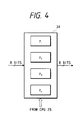
- the gamma conversion unit 34 which has the structure shown in Fig. 4, is a table conversion circuit in which one of the gamma conversion characteristics ⁇ 1 to ⁇ 4 is selected responsive to a selection signal from the CPU 25.
- This table conversion circuit can be realized by, e.g., causing an ROM to store input and output characteristics of ⁇ 1 to ⁇ 4. Further, if the table conversion circuit is realized by an RAM, a gamma conversion table may be formed according to the membrane thickness in such a manner that a set of table data of the characteristic to be selected is set in the RAM by the CPU 25.
- the constant output density characteristic can be obtained irrespective of the membrane thickness of the photosensitive body.
- the density characteristic of the image data representing an image for reproduction is converted based on the membrane thickness of the photosensitive body, while the parameter such as the developing bias or the like in the image forming process is not changed based on the value according to the membrane thickness, so that the image forming characteristic of the printer is fixed and the tonality characteristic including an intermediate level can be well controlled.
- Fig. 8 shows a result obtained by performing a following primary conversion of a density signal, instead of a non-linear conversion by a density conversion table.
- D out A ⁇ (D in + B)
- Fig. 9 shows output density characteristics in a case where correcting by an image signal process circuit (or apparatus) 4 is not performed when a temperature and a humidity of a photosensitive drum is set as 15°C5%RH, 23°C60%RH and 30°C80%RH.
- Fig. 10 shows output density characteristics in a case where the temperature of the photosensitive drum is detected by a temperature and humidity sensor and then density signal converting by using a density conversion table is performed in the image signal process circuit 4 on the basis of a detection output.
- the constant output density characteristics can be obtained irrespective of the temperature and the humidity of the photosensitive drum.
- Fig. 11 shows a result obtained by performing correcting in an image signal process circuit (or apparatus) 4 in a case where a temperature and a humidity of a photosensitive drum is set as 15°C5%RH, 23°C60%RH and 30°C80%RH, by using a primary conversion of a density signal instead of a density conversion table. Also in such a case, it can be understood that substantially constant output density characteristics can be obtained.
- a timing of detecting the membrane thickness in the first embodiment for example, there can be used a pre- and multi-rotation of the drum due to on/off of the power source of the image forming apparatus, a pre-rotation time of the image support body (before the image forming), and a post-rotation time of the image support body (after the image forming).
- a pre-rotation time of the image support body before the image forming
- a post-rotation time of the image support body after the image forming.
- the detection timing increasingly follows changes in a photosensitive body, and also increasingly follows a case where the photosensitive body which has been used for a long period of time is changed to new one.
- the life of the photosensitive body is shortened and the throughput as the image forming apparatus is decreased, and at the same time the detection timing well follows the change in the membrane thickness of the photosensitive body, especially the abrupt change caused by exchanging the photosensitive body.
- the membrane thickness of the photosensitive body reduces to the extent of 13 ⁇ m, a crack or a flaw begins to occur on the photosensitive drum and thus a faulty image is output, so that it is necessary to change the photosensitive drum 6 into new one.
- the detecting of the photosensitive body membrane thickness should be performed in the post-rotation of the drum after the image forming corresponding to about 500 to 1,000 sheets to prolong the life of the photosensitive drum 6 to some extent. Such the detecting of the membrane thickness at the post-rotation time is performed accurately by using an enough time of about ten seconds.
- the image forming is performed by using the gamma conversion table which has been optimized to a state where the membrane thickness of the photosensitive drum 6 is thin, during the image forming between 500 to 1,000 sheets.
- the gamma conversion table for the membrane thickness of 13 ⁇ m is used for the photosensitive drum having the membrane thickness of 30 ⁇ m, inclination of the curve of the output image density for the original density becomes abrupt, so that a deviation from a linear line becomes large.
- a CPU 25 detects the membrane thickness of the photosensitive body and selects the gamma conversion table in accordance with a flow chart shown in Fig. 12.
- the fundamental structure for performing such operations is the same as that in the first embodiment.
- a power-on state or an open/close state of a front door for exchanging the photosensitive drum is detected (step S1). If detected, in response to a turned-on state of a copy switch (step S2), the membrane thickness of the photosensitive body is detected in the pre-rotation before the image forming (step S3). Since such the membrane thickness detecting in the pre-rotation is performed for a short period of time (1 to 2 seconds), the life of the drum is not so affected, but the detection accuracy is low. Then, an absolute value of a difference between a detection signal DT 2 which is obtained in such the detecting and a previously-stored detection signal DTM which is obtained when the previous gamma conversion table was changed (step S4).
- the gamma conversion table is changed by using the detection signal DT 2 in the same manner as that described in the first embodiment (steps S5 to S11, and S31).
- a predetermined threshold value dDT 2 about 5 ⁇ m to 10 ⁇ m
- a count value TDN obtained by counting the number of copies is set as "501" for the detecting of the photosensitive body membrane thickness in the post-rotation after the subsequent image forming (step S12).
- the suitable gamma conversion table can be selected by the less number of detection times, the short period of time and the highly accurate membrane thickness measuring.
- a primary converting may be used instead of the gamma conversion table changing in the present embodiment.
- the gamma conversion table is selected on the basis of the one-time detecting.
- the gamma conversion table may be selected on the basis of a result obtained through a plurality of detecting. For example, if the gamma conversion table is changed when the detection signal T D exceeds one threshold value accumulatively three times, the highly accurate optimization of the gamma table becomes possible.
- the value according to the membrane thickness of the photosensitive body is a value strictly representing the membrane thickness itself. That is, such the value may be a value which changes according to the change in the membrane thickness.
- the photosensitive body is not limited to the photosensitive drum, but may be a photosensitive belt.
- the developing bias is exceptionally controlled according to the signal T D .
- the signal T D may be always managed independently of the developing bias.
Landscapes
- Physics & Mathematics (AREA)
- General Physics & Mathematics (AREA)
- Engineering & Computer Science (AREA)
- Plasma & Fusion (AREA)
- Multimedia (AREA)
- Signal Processing (AREA)
- Control Or Security For Electrophotography (AREA)
Applications Claiming Priority (3)
| Application Number | Priority Date | Filing Date | Title |
|---|---|---|---|
| JP280426/95 | 1995-10-27 | ||
| JP28042695 | 1995-10-27 | ||
| JP28042695 | 1995-10-27 |
Publications (3)
| Publication Number | Publication Date |
|---|---|
| EP0770929A2 true EP0770929A2 (fr) | 1997-05-02 |
| EP0770929A3 EP0770929A3 (fr) | 1997-05-21 |
| EP0770929B1 EP0770929B1 (fr) | 2005-04-13 |
Family
ID=17624895
Family Applications (1)
| Application Number | Title | Priority Date | Filing Date |
|---|---|---|---|
| EP96307728A Expired - Lifetime EP0770929B1 (fr) | 1995-10-27 | 1996-10-25 | Appareil de formation d'images |
Country Status (3)
| Country | Link |
|---|---|
| US (1) | US5726759A (fr) |
| EP (1) | EP0770929B1 (fr) |
| DE (1) | DE69634588T2 (fr) |
Families Citing this family (4)
| Publication number | Priority date | Publication date | Assignee | Title |
|---|---|---|---|---|
| JP3416383B2 (ja) * | 1996-03-05 | 2003-06-16 | キヤノン株式会社 | 画像形成装置 |
| JP3804113B2 (ja) * | 1996-08-26 | 2006-08-02 | コニカミノルタホールディングス株式会社 | 固体撮像装置 |
| JPH10161402A (ja) * | 1996-11-27 | 1998-06-19 | Minolta Co Ltd | 画像形成装置 |
| US6771839B2 (en) * | 2001-02-20 | 2004-08-03 | Sharp Laboratories Of America, Inc. | Efficient method of computing gamma correction tables |
Family Cites Families (11)
| Publication number | Priority date | Publication date | Assignee | Title |
|---|---|---|---|---|
| DE3408336A1 (de) * | 1983-03-08 | 1984-09-13 | Canon K.K., Tokio/Tokyo | Bildreproduktionssystem |
| JPH0698769B2 (ja) * | 1985-11-15 | 1994-12-07 | キヤノン株式会社 | 記録装置 |
| US4794413A (en) * | 1986-08-20 | 1988-12-27 | Canon Kabushiki Kaisha | Image recording apparatus |
| JP2607490B2 (ja) * | 1986-12-09 | 1997-05-07 | キヤノン株式会社 | 画像形成装置の画質制御方法 |
| US4989039A (en) * | 1987-01-19 | 1991-01-29 | Canon Kabushiki Kaisha | Image forming apparatus responsive to environmental conditions |
| US5056042A (en) * | 1990-04-02 | 1991-10-08 | Calcomp Inc. | Media conductivity-based pulse controller for electrostatic printer |
| JPH04212181A (ja) * | 1990-06-14 | 1992-08-03 | Sharp Corp | 感光体膜減り検出装置を備える画像形成装置 |
| US5305057A (en) * | 1991-07-05 | 1994-04-19 | Minolta Camera Kabushiki Kaisha | Image forming apparatus having correction means for modifying image density signals according to a gradation correction table |
| DE69325113T2 (de) * | 1992-02-07 | 1999-11-04 | Canon K.K., Tokio/Tokyo | Bilderzeugungsgerät mit einem Auflade-Element in Kontakt mit dem Bildträgerelement |
| EP0568352B1 (fr) * | 1992-04-28 | 1998-10-28 | Canon Kabushiki Kaisha | Appareil de formation d'images comprenant un élément de chargement |
| JPH0761044A (ja) * | 1993-08-31 | 1995-03-07 | Sony Corp | プリンタ |
-
1996
- 1996-10-24 US US08/736,479 patent/US5726759A/en not_active Expired - Lifetime
- 1996-10-25 DE DE69634588T patent/DE69634588T2/de not_active Expired - Lifetime
- 1996-10-25 EP EP96307728A patent/EP0770929B1/fr not_active Expired - Lifetime
Non-Patent Citations (1)
| Title |
|---|
| None |
Also Published As
| Publication number | Publication date |
|---|---|
| EP0770929A3 (fr) | 1997-05-21 |
| DE69634588D1 (de) | 2005-05-19 |
| US5726759A (en) | 1998-03-10 |
| DE69634588T2 (de) | 2006-02-09 |
| EP0770929B1 (fr) | 2005-04-13 |
Similar Documents
| Publication | Publication Date | Title |
|---|---|---|
| US5305057A (en) | Image forming apparatus having correction means for modifying image density signals according to a gradation correction table | |
| US5749022A (en) | Charging apparatus and method for use in image forming device | |
| US6501917B1 (en) | Method and apparatus for image forming capable of effectively performing image density adjustment | |
| US5574544A (en) | Image forming apparatus having image density gradation correction means | |
| US5684685A (en) | High voltage power supply for image transfer and image forming apparatus using the same | |
| GB2248038A (en) | Condition responsive optimisation of photoelectrostatic printing machine | |
| JP3715758B2 (ja) | 画像形成装置 | |
| US5726759A (en) | Image forming apparatus | |
| JPS60260066A (ja) | 電子写真の制御方法 | |
| US5574543A (en) | Image forming apparatus | |
| JPH0444271B2 (fr) | ||
| US5819131A (en) | Technique for controlling the developing voltage to accomodate the environment | |
| JP2007140431A (ja) | 画像形成装置 | |
| JPH08234635A (ja) | 画像形成装置 | |
| CA2134247A1 (fr) | Methode et appareil de controle du fond dans une imprimante electrostatographique | |
| US6510293B1 (en) | Image forming apparatus having toner density detection and image density control method therefore | |
| JPH08123110A (ja) | 画像形成装置およびその画像濃度制御方法 | |
| JPH0754957B2 (ja) | 記録装置の光量制御装置 | |
| JP3227822B2 (ja) | 作像装置 | |
| US5060022A (en) | Image processing equipment for setting image density conditions according to temperature | |
| JPH10288875A (ja) | 画像形成装置 | |
| JPS61156265A (ja) | 画像形成装置 | |
| JPH09179448A (ja) | 画像形成装置 | |
| JP3610214B2 (ja) | 画像形成装置 | |
| JP3264676B2 (ja) | 画像形成装置 |
Legal Events
| Date | Code | Title | Description |
|---|---|---|---|
| PUAI | Public reference made under article 153(3) epc to a published international application that has entered the european phase |
Free format text: ORIGINAL CODE: 0009012 |
|
| PUAL | Search report despatched |
Free format text: ORIGINAL CODE: 0009013 |
|
| AK | Designated contracting states |
Kind code of ref document: A2 Designated state(s): DE FR GB IT |
|
| AK | Designated contracting states |
Kind code of ref document: A3 Designated state(s): DE FR GB IT |
|
| 17P | Request for examination filed |
Effective date: 19971002 |
|
| 17Q | First examination report despatched |
Effective date: 20000802 |
|
| GRAP | Despatch of communication of intention to grant a patent |
Free format text: ORIGINAL CODE: EPIDOSNIGR1 |
|
| GRAS | Grant fee paid |
Free format text: ORIGINAL CODE: EPIDOSNIGR3 |
|
| GRAA | (expected) grant |
Free format text: ORIGINAL CODE: 0009210 |
|
| AK | Designated contracting states |
Kind code of ref document: B1 Designated state(s): DE FR GB IT |
|
| PG25 | Lapsed in a contracting state [announced via postgrant information from national office to epo] |
Ref country code: IT Free format text: LAPSE BECAUSE OF FAILURE TO SUBMIT A TRANSLATION OF THE DESCRIPTION OR TO PAY THE FEE WITHIN THE PRESCRIBED TIME-LIMIT;WARNING: LAPSES OF ITALIAN PATENTS WITH EFFECTIVE DATE BEFORE 2007 MAY HAVE OCCURRED AT ANY TIME BEFORE 2007. THE CORRECT EFFECTIVE DATE MAY BE DIFFERENT FROM THE ONE RECORDED. Effective date: 20050413 |
|
| REG | Reference to a national code |
Ref country code: GB Ref legal event code: FG4D |
|
| REF | Corresponds to: |
Ref document number: 69634588 Country of ref document: DE Date of ref document: 20050519 Kind code of ref document: P |
|
| PLBE | No opposition filed within time limit |
Free format text: ORIGINAL CODE: 0009261 |
|
| STAA | Information on the status of an ep patent application or granted ep patent |
Free format text: STATUS: NO OPPOSITION FILED WITHIN TIME LIMIT |
|
| 26N | No opposition filed |
Effective date: 20060116 |
|
| EN | Fr: translation not filed | ||
| PG25 | Lapsed in a contracting state [announced via postgrant information from national office to epo] |
Ref country code: FR Free format text: LAPSE BECAUSE OF NON-PAYMENT OF DUE FEES Effective date: 20051031 |
|
| PG25 | Lapsed in a contracting state [announced via postgrant information from national office to epo] |
Ref country code: FR Free format text: LAPSE BECAUSE OF NON-PAYMENT OF DUE FEES Effective date: 20050413 |
|
| PGFP | Annual fee paid to national office [announced via postgrant information from national office to epo] |
Ref country code: DE Payment date: 20121031 Year of fee payment: 17 |
|
| PGFP | Annual fee paid to national office [announced via postgrant information from national office to epo] |
Ref country code: GB Payment date: 20121016 Year of fee payment: 17 |
|
| GBPC | Gb: european patent ceased through non-payment of renewal fee |
Effective date: 20131025 |
|
| PG25 | Lapsed in a contracting state [announced via postgrant information from national office to epo] |
Ref country code: GB Free format text: LAPSE BECAUSE OF NON-PAYMENT OF DUE FEES Effective date: 20131025 |
|
| REG | Reference to a national code |
Ref country code: DE Ref legal event code: R119 Ref document number: 69634588 Country of ref document: DE Effective date: 20140501 |
|
| PG25 | Lapsed in a contracting state [announced via postgrant information from national office to epo] |
Ref country code: DE Free format text: LAPSE BECAUSE OF NON-PAYMENT OF DUE FEES Effective date: 20140501 |