EP0772301A2 - Circuit pour stabiliser la sortie d'un circuit à trois états - Google Patents
Circuit pour stabiliser la sortie d'un circuit à trois états Download PDFInfo
- Publication number
- EP0772301A2 EP0772301A2 EP96117258A EP96117258A EP0772301A2 EP 0772301 A2 EP0772301 A2 EP 0772301A2 EP 96117258 A EP96117258 A EP 96117258A EP 96117258 A EP96117258 A EP 96117258A EP 0772301 A2 EP0772301 A2 EP 0772301A2
- Authority
- EP
- European Patent Office
- Prior art keywords
- circuit
- tri
- output
- state
- stabilizing
- Prior art date
- Legal status (The legal status is an assumption and is not a legal conclusion. Google has not performed a legal analysis and makes no representation as to the accuracy of the status listed.)
- Ceased
Links
Images
Classifications
-
- H—ELECTRICITY
- H03—ELECTRONIC CIRCUITRY
- H03K—PULSE TECHNIQUE
- H03K19/00—Logic circuits, i.e. having at least two inputs acting on one output; Inverting circuits
-
- H—ELECTRICITY
- H03—ELECTRONIC CIRCUITRY
- H03K—PULSE TECHNIQUE
- H03K19/00—Logic circuits, i.e. having at least two inputs acting on one output; Inverting circuits
- H03K19/0008—Arrangements for reducing power consumption
- H03K19/0016—Arrangements for reducing power consumption by using a control or a clock signal, e.g. in order to apply power supply
-
- H—ELECTRICITY
- H03—ELECTRONIC CIRCUITRY
- H03K—PULSE TECHNIQUE
- H03K19/00—Logic circuits, i.e. having at least two inputs acting on one output; Inverting circuits
- H03K19/02—Logic circuits, i.e. having at least two inputs acting on one output; Inverting circuits using specified components
- H03K19/08—Logic circuits, i.e. having at least two inputs acting on one output; Inverting circuits using specified components using semiconductor devices
- H03K19/094—Logic circuits, i.e. having at least two inputs acting on one output; Inverting circuits using specified components using semiconductor devices using field-effect transistors
- H03K19/09425—Multistate logic
- H03K19/09429—Multistate logic one of the states being the high impedance or floating state
Definitions
- the present invention relates to a circuit for stabilizing the output of a tri-state circuit, and more particularly to circuits which can stabilize the output of the tri-state circuit whilst removing unwanted current paths.
- CMOS logic devices have a high impedance state which is caused by timing mismatch during dynamic operation and by a delay value. Such a high impedance state causes unstable operation of the device, sometimes resulting in malfunction of the device.
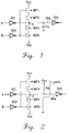
- Fig. 1 shows the construction of a typical tri-state circuit.
- this circuit outputs a logic "low” signal or a logic “high” signal according to the logic states of the input signals. That is, if the input signals A and B are both at the logic “low” level, these signals are inverted to logic "high” levels via inverters IG1 and IG2. Then, PMOS transistors MP1 and MP2 are turned off, while NMOS transistors MN1 and MN2 are turned on. Thus, the output signal Y of the tri-state circuit goes to the logic "low” level. If the input signals A and B are both at the logic "high” level, the output signal Y goes to the logic "high” level.
- the output node enters a floating state.
- the floating state can be prevented by adding a pull-up circuit or a pull-down circuit as shown in Fig. 2.
- Fig. 2 shows a conventional circuit for stabilizing the output of the tri-state circuit as shown in Fig. 1 by using a pull-up method, however, it is also possible to prevent the floating by using a pull-down method in a similar way as described above.
- an unnecessary current path is formed when the output signal Y is at the logic "low” level
- an unnecessary current path is formed when the output signal Y is at the logic "high” level.
- the present invention provides a stabilizing circuit for stabilizing the output of a tri-state circuit which has at least two input terminals for receiving at least two input signals and an output terminal which enters a high impedance state when the input signals take on a given combination or one of a number of given combinations, the stabilizing circuit comprising:
- the output signal is a single output line and the first and second class of signals are first and second logic levels.
- the means for pulling the output terminal of the tri-state circuit up or down may comprise a MOS transistor having its channel connected between the output terminal and the said predetermined voltage level and its gate connected to the said output line.
- the second input signal is a control signal and the output terminal enters a high impedance state when the first input signal and the control signal are at different logic logic levels.
- the said logic circuit may be an XOR or an XNOR circuit.
- the said logic circuit is an XOR circuit and the means for pulling the output terminal of the tri-state circuit up or down comprises an NMOS transistor having its channel connected between the output terminal and the said predetermined voltage level and its gate connected to the said output line.
- the said predetermined voltage may be ground potential.
- the said logic circuit is an XNOR circuit and the means for pulling the output terminal of the tri-state circuit up or down comprises a PMOS transistor having its channel connected between the output terminal and the said predetermined voltage level and its gate connected to the said output line.
- the said predetermined voltage may be a power supply voltage level.
- the present invention also extends to a tri-state circuit having at least two input terminals for receiving at least two input signals and an output terminal which enters a high impedance state when the input signals take on a given combination or one of a number of given combinations provided with a stabilizing circuit according to any preceding claim for stabilizing its output.
- the tri-state circuit may comprise:
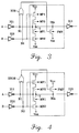
- Fig. 3 is a circuit diagram showing a circuit for stabilizing the output of a tri-state circuit using a pull-down method according to the present invention.
- first and second input signals A and B are inverted via inverters IG1 and 1G2 and then are applied to first and second input nodes N1 and N2, respectively.
- the second input signal B is used as a control signal.
- the tri-state circuit comprises a buffer circuit with an inverter construction and a control circuit.
- the buffer circuit comprising a PMOS transistor MP2 and an NMOS transistor MN1 is connected between the first input node N1 and an output node INA.
- the control circuit comprises a PMOS transistor MP1 connected between a power supply voltage Vcc and the source of the PMOS transistor MP2 and an NMOS transistor MN2 connected between the source of the NMOS transistor MN1 and a ground voltage Vss.
- the gates of the PMOS transistor MP1 and NMOS transistor MN2 are connected to the second input node N2.
- a pull-down transistor PMN is connected between the output node INA and ground potential Vss and has a gate connected to the output of an exclusive OR gate XOR.
- the exclusive OR gate XOR exclusively ORs two inverted input signals A ⁇ and B ⁇ and then applies the result to the gate of the pull-down transistor PMN.
- the pull-down transistor PMN is turned off by the output of the exclusive OR gate XOR, thus enabling the isolation of the current path.
- Fig. 4 shows a circuit for stabilizing the output of the tri-state circuit using the pull-up method according to the present invention.
- First and second input signals A and B are inverted via inverters IG1 and IG2 and then applied to first and second input nodes N1 and N2, respectively.
- the tri-state circuit comprises a buffer circuit with an inverter construction and a control circuit.
- the buffer circuit comprising a PMOS transistor MP2 and an NMOS transistor MN1 is connected to the first input node N1.
- the control circuit comprises a PMOS transistor MP1 connected between the power supply voltage Vcc and the source of the PMOS transistor MP2 and an NMOS transistor MN2 connected between the source of the NMOS transistor MN1 and ground potential Vss.
- a pull-up transistor PMP is connected between the power supply voltage Vcc and the output node INA and has a gate connected to the output terminal of an exclusive NOR gate XNOR.
- the exclusive NOR gate XNOR exclusively NORs two input signals A ⁇ and B ⁇ from the first and second input nodes N1 and N2 and then applies the result to the gate of the pull-up transistor PMP.
- the pull-up transistor PMP is turned off by the exclusive NOR gate XNOR, thus enabling the isolation of the current path.
- the circuit for stabilizing the output of the tri-state circuit can stabilize the operation of the tri-state circuit by preventing the floating state and can isolate unnecessary current paths, thus reducing power consumption.
Landscapes
- Engineering & Computer Science (AREA)
- Physics & Mathematics (AREA)
- Computer Hardware Design (AREA)
- Computing Systems (AREA)
- General Engineering & Computer Science (AREA)
- Mathematical Physics (AREA)
- Power Engineering (AREA)
- Logic Circuits (AREA)
Applications Claiming Priority (2)
| Application Number | Priority Date | Filing Date | Title |
|---|---|---|---|
| KR1019950039608A KR100255962B1 (ko) | 1995-11-03 | 1995-11-03 | 3-상태회로의 출력 안정화회로 |
| KR3960895 | 1995-11-03 |
Publications (2)
| Publication Number | Publication Date |
|---|---|
| EP0772301A2 true EP0772301A2 (fr) | 1997-05-07 |
| EP0772301A3 EP0772301A3 (fr) | 1998-04-01 |
Family
ID=19432898
Family Applications (1)
| Application Number | Title | Priority Date | Filing Date |
|---|---|---|---|
| EP96117258A Ceased EP0772301A3 (fr) | 1995-11-03 | 1996-10-28 | Circuit pour stabiliser la sortie d'un circuit à trois états |
Country Status (4)
| Country | Link |
|---|---|
| US (1) | US5767696A (fr) |
| EP (1) | EP0772301A3 (fr) |
| JP (1) | JP3644468B2 (fr) |
| KR (1) | KR100255962B1 (fr) |
Cited By (1)
| Publication number | Priority date | Publication date | Assignee | Title |
|---|---|---|---|---|
| WO2003100976A1 (fr) * | 2002-05-24 | 2003-12-04 | Qualcomm, Incorporated | Circuit delivrant un potentiel determine sur une borne de sortie d'un circuit logique hors tension |
Families Citing this family (6)
| Publication number | Priority date | Publication date | Assignee | Title |
|---|---|---|---|---|
| US5767709A (en) * | 1996-01-19 | 1998-06-16 | Sgs-Thomson Microelectronics, Inc. | Synchronous test mode initalization |
| US5955898A (en) * | 1997-06-30 | 1999-09-21 | Sun Microsystems, Inc. | Selector and decision wait using pass gate XOR |
| US6366123B1 (en) * | 2001-02-05 | 2002-04-02 | Etron Technology, Inc. | Input buffer circuit for low power application |
| US7075976B1 (en) * | 2001-03-19 | 2006-07-11 | Cisco Technology, Inc. | Tri-state transmitter |
| JP5326927B2 (ja) * | 2009-08-19 | 2013-10-30 | 富士電機株式会社 | レベルシフト回路 |
| JP5402852B2 (ja) * | 2009-12-04 | 2014-01-29 | 富士電機株式会社 | レベルシフト回路 |
Citations (7)
| Publication number | Priority date | Publication date | Assignee | Title |
|---|---|---|---|---|
| JPS6054519A (ja) * | 1983-09-05 | 1985-03-29 | Matsushita Electric Ind Co Ltd | 入出力回路 |
| US4523292A (en) * | 1982-09-30 | 1985-06-11 | Rca Corporation | Complementary FET ripple carry binary adder circuit |
| US4685079A (en) * | 1984-12-14 | 1987-08-04 | Rca Corporation | Ripple-borrow binary subtraction circuit |
| US4761760A (en) * | 1984-08-17 | 1988-08-02 | Nec Corporation | Digital adder-subtracter with tentative result correction circuit |
| EP0291963A2 (fr) * | 1987-05-20 | 1988-11-23 | CSELT Centro Studi e Laboratori Telecomunicazioni S.p.A. | Additionneur rapide à CMOS |
| JPH06120804A (ja) * | 1992-10-06 | 1994-04-28 | Hitachi Ltd | トライステート形出力回路 |
| DE4342639C1 (de) * | 1993-12-14 | 1995-04-27 | Siemens Ag | Volladdierstufe und Verwendung |
Family Cites Families (9)
| Publication number | Priority date | Publication date | Assignee | Title |
|---|---|---|---|---|
| JPS6041325A (ja) * | 1983-08-16 | 1985-03-05 | Nec Corp | 半導体集積回路 |
| JPS60103826A (ja) * | 1983-11-11 | 1985-06-08 | Nec Corp | 論理回路 |
| US4749886A (en) * | 1986-10-09 | 1988-06-07 | Intersil, Inc. | Reduced parallel EXCLUSIVE or and EXCLUSIVE NOR gate |
| US4928023A (en) * | 1987-08-27 | 1990-05-22 | Texas Instruments Incorporated | Improved output buffer having reduced noise characteristics |
| JPH0316427A (ja) * | 1989-06-14 | 1991-01-24 | Seiko Epson Corp | 入出力兼用装置 |
| US4968903A (en) * | 1989-08-03 | 1990-11-06 | Motorola Inc. | Combinational static CMOS logic circuit |
| JP2567172B2 (ja) * | 1992-01-09 | 1996-12-25 | 株式会社東芝 | 半導体回路の出力段に配置される出力回路 |
| US5334888A (en) * | 1993-04-19 | 1994-08-02 | Intel Corporation | Fast exclusive-or and exclusive-nor gates |
| US5568062A (en) * | 1995-07-14 | 1996-10-22 | Kaplinsky; Cecil H. | Low noise tri-state output buffer |
-
1995
- 1995-11-03 KR KR1019950039608A patent/KR100255962B1/ko not_active Expired - Lifetime
-
1996
- 1996-10-28 EP EP96117258A patent/EP0772301A3/fr not_active Ceased
- 1996-11-01 US US08/742,721 patent/US5767696A/en not_active Expired - Lifetime
- 1996-11-05 JP JP29231996A patent/JP3644468B2/ja not_active Expired - Lifetime
Patent Citations (7)
| Publication number | Priority date | Publication date | Assignee | Title |
|---|---|---|---|---|
| US4523292A (en) * | 1982-09-30 | 1985-06-11 | Rca Corporation | Complementary FET ripple carry binary adder circuit |
| JPS6054519A (ja) * | 1983-09-05 | 1985-03-29 | Matsushita Electric Ind Co Ltd | 入出力回路 |
| US4761760A (en) * | 1984-08-17 | 1988-08-02 | Nec Corporation | Digital adder-subtracter with tentative result correction circuit |
| US4685079A (en) * | 1984-12-14 | 1987-08-04 | Rca Corporation | Ripple-borrow binary subtraction circuit |
| EP0291963A2 (fr) * | 1987-05-20 | 1988-11-23 | CSELT Centro Studi e Laboratori Telecomunicazioni S.p.A. | Additionneur rapide à CMOS |
| JPH06120804A (ja) * | 1992-10-06 | 1994-04-28 | Hitachi Ltd | トライステート形出力回路 |
| DE4342639C1 (de) * | 1993-12-14 | 1995-04-27 | Siemens Ag | Volladdierstufe und Verwendung |
Non-Patent Citations (2)
| Title |
|---|
| Computer translation of JP-A-6 120 804 obtained from the internet page of the JPO 31.08.2000 * |
| PATENT ABSTRACTS OF JAPAN vol. 018, no. 406 (E - 1585) 28 July 1994 (1994-07-28) * |
Cited By (1)
| Publication number | Priority date | Publication date | Assignee | Title |
|---|---|---|---|---|
| WO2003100976A1 (fr) * | 2002-05-24 | 2003-12-04 | Qualcomm, Incorporated | Circuit delivrant un potentiel determine sur une borne de sortie d'un circuit logique hors tension |
Also Published As
| Publication number | Publication date |
|---|---|
| JPH09172365A (ja) | 1997-06-30 |
| EP0772301A3 (fr) | 1998-04-01 |
| KR970031312A (ko) | 1997-06-26 |
| KR100255962B1 (ko) | 2000-05-01 |
| JP3644468B2 (ja) | 2005-04-27 |
| US5767696A (en) | 1998-06-16 |
Similar Documents
| Publication | Publication Date | Title |
|---|---|---|
| US5361002A (en) | Voltage compensating CMOS input buffer | |
| EP0908005B1 (fr) | Amplificateur differentiel | |
| KR100591520B1 (ko) | 감소된 전압 입출력의 3상태 버퍼 및 그 제조 방법 | |
| US5914844A (en) | Overvoltage-tolerant input-output buffers having a switch configured to isolate a pull up transistor from a voltage supply | |
| EP0405833A2 (fr) | Tampon à niveaux logiques d'entrée programmables | |
| EP0847623B1 (fr) | Tampon de sortie a noeuds intermediaires partages | |
| EP1014581B1 (fr) | Circuit d'attaque à puissance réglable et méthode de réglage | |
| KR100218336B1 (ko) | 레벨 시프터 | |
| US5929679A (en) | Voltage monitoring circuit capable of reducing power dissipation | |
| US6049242A (en) | Voltage reference source for an overvoltage-tolerant bus interface | |
| JPH0389624A (ja) | 半導体集積回路 | |
| EP0772301A2 (fr) | Circuit pour stabiliser la sortie d'un circuit à trois états | |
| US4503341A (en) | Power-down inverter circuit | |
| EP0386570A1 (fr) | Translateur de niveaux logiques TTL/CMOS | |
| US5894227A (en) | Level restoration circuit for pass logic devices | |
| US20070279091A1 (en) | Digital Voltage Level Shifter | |
| US5495182A (en) | Fast-fully restoring polarity control circuit | |
| US5530401A (en) | Single source differential circuit | |
| US5177377A (en) | Bi-CMOS circuit | |
| US5455520A (en) | CMOS input circuit for providing logical output signal from TTL compatible input signal | |
| KR960008137B1 (ko) | 반도체 소자의 노이즈 특성 강화회로 | |
| JPH066186A (ja) | ラッチ回路 | |
| US6329842B1 (en) | Output circuit for electronic devices | |
| US6198306B1 (en) | CMOS waveshaping buffer | |
| KR100190303B1 (ko) | 반도체 메모리소자의 출력 버퍼 |
Legal Events
| Date | Code | Title | Description |
|---|---|---|---|
| PUAI | Public reference made under article 153(3) epc to a published international application that has entered the european phase |
Free format text: ORIGINAL CODE: 0009012 |
|
| 17P | Request for examination filed |
Effective date: 19961028 |
|
| AK | Designated contracting states |
Kind code of ref document: A2 Designated state(s): DE FR GB NL |
|
| PUAL | Search report despatched |
Free format text: ORIGINAL CODE: 0009013 |
|
| AK | Designated contracting states |
Kind code of ref document: A3 Designated state(s): DE FR GB NL |
|
| 17Q | First examination report despatched |
Effective date: 20000322 |
|
| STAA | Information on the status of an ep patent application or granted ep patent |
Free format text: STATUS: THE APPLICATION HAS BEEN REFUSED |
|
| 18R | Application refused |
Effective date: 20020629 |