EP0779768A2 - Procédé et circuit pour alimenter une lampe à décharge - Google Patents
Procédé et circuit pour alimenter une lampe à décharge Download PDFInfo
- Publication number
- EP0779768A2 EP0779768A2 EP96118851A EP96118851A EP0779768A2 EP 0779768 A2 EP0779768 A2 EP 0779768A2 EP 96118851 A EP96118851 A EP 96118851A EP 96118851 A EP96118851 A EP 96118851A EP 0779768 A2 EP0779768 A2 EP 0779768A2
- Authority
- EP
- European Patent Office
- Prior art keywords
- circuit
- clock generator
- current
- load current
- phase
- Prior art date
- Legal status (The legal status is an assumption and is not a legal conclusion. Google has not performed a legal analysis and makes no representation as to the accuracy of the status listed.)
- Granted
Links
- 238000000034 method Methods 0.000 title claims description 25
- 230000008569 process Effects 0.000 title description 6
- 239000003990 capacitor Substances 0.000 claims abstract description 31
- 238000001514 detection method Methods 0.000 claims description 20
- 230000010355 oscillation Effects 0.000 claims description 12
- 101500011075 Diploptera punctata Allatostatin-7 Proteins 0.000 claims description 8
- 101100194362 Schizosaccharomyces pombe (strain 972 / ATCC 24843) res1 gene Proteins 0.000 claims description 8
- 101100194363 Schizosaccharomyces pombe (strain 972 / ATCC 24843) res2 gene Proteins 0.000 claims description 7
- 230000001105 regulatory effect Effects 0.000 claims description 7
- 101100270983 Arabidopsis thaliana ASE3 gene Proteins 0.000 claims description 5
- 230000009849 deactivation Effects 0.000 claims description 3
- 230000004913 activation Effects 0.000 claims description 2
- 230000001276 controlling effect Effects 0.000 claims description 2
- 230000001360 synchronised effect Effects 0.000 abstract description 3
- 230000008033 biological extinction Effects 0.000 abstract 1
- 238000009795 derivation Methods 0.000 abstract 1
- 238000005259 measurement Methods 0.000 abstract 1
- 101100481028 Arabidopsis thaliana TGA2 gene Proteins 0.000 description 11
- 101000829425 Homo sapiens Steroid receptor RNA activator 1 Proteins 0.000 description 8
- 101000711846 Homo sapiens Transcription factor SOX-9 Proteins 0.000 description 8
- 101100481019 Nicotiana tabacum TGA1A gene Proteins 0.000 description 8
- 102100027779 Splicing factor, arginine/serine-rich 19 Human genes 0.000 description 8
- 101150092207 TGA1 gene Proteins 0.000 description 8
- 230000008901 benefit Effects 0.000 description 8
- 230000007423 decrease Effects 0.000 description 6
- 230000008859 change Effects 0.000 description 4
- 102100027479 DNA-directed RNA polymerase I subunit RPA34 Human genes 0.000 description 3
- 101001068636 Homo sapiens Protein regulator of cytokinesis 1 Proteins 0.000 description 3
- 238000010586 diagram Methods 0.000 description 3
- 230000010354 integration Effects 0.000 description 3
- 101100489887 Arabidopsis thaliana ABA2 gene Proteins 0.000 description 2
- 101100270982 Arabidopsis thaliana ASE2 gene Proteins 0.000 description 2
- 101500011077 Diploptera punctata Allatostatin-9 Proteins 0.000 description 2
- 101100160925 Gibberella zeae (strain ATCC MYA-4620 / CBS 123657 / FGSC 9075 / NRRL 31084 / PH-1) ZEA1 gene Proteins 0.000 description 2
- 101100160926 Gibberella zeae (strain ATCC MYA-4620 / CBS 123657 / FGSC 9075 / NRRL 31084 / PH-1) ZEA2 gene Proteins 0.000 description 2
- 101100501251 Saccharomyces cerevisiae (strain ATCC 204508 / S288c) ELO3 gene Proteins 0.000 description 2
- 101100478321 Schizosaccharomyces pombe (strain 972 / ATCC 24843) sre2 gene Proteins 0.000 description 2
- 230000015572 biosynthetic process Effects 0.000 description 2
- 238000013016 damping Methods 0.000 description 2
- 101150036683 sre1 gene Proteins 0.000 description 2
- 230000007704 transition Effects 0.000 description 2
- 238000004804 winding Methods 0.000 description 2
- 238000013459 approach Methods 0.000 description 1
- 230000003247 decreasing effect Effects 0.000 description 1
- 230000001934 delay Effects 0.000 description 1
- 230000000694 effects Effects 0.000 description 1
- 238000005516 engineering process Methods 0.000 description 1
- 230000007613 environmental effect Effects 0.000 description 1
- 230000005669 field effect Effects 0.000 description 1
- 238000007667 floating Methods 0.000 description 1
- 230000004907 flux Effects 0.000 description 1
- 238000009499 grossing Methods 0.000 description 1
- 238000010438 heat treatment Methods 0.000 description 1
- 238000004519 manufacturing process Methods 0.000 description 1
- 239000004065 semiconductor Substances 0.000 description 1
- 230000001629 suppression Effects 0.000 description 1
Images


Classifications
-
- H—ELECTRICITY
- H05—ELECTRIC TECHNIQUES NOT OTHERWISE PROVIDED FOR
- H05B—ELECTRIC HEATING; ELECTRIC LIGHT SOURCES NOT OTHERWISE PROVIDED FOR; CIRCUIT ARRANGEMENTS FOR ELECTRIC LIGHT SOURCES, IN GENERAL
- H05B41/00—Circuit arrangements or apparatus for igniting or operating discharge lamps
- H05B41/14—Circuit arrangements
- H05B41/26—Circuit arrangements in which the lamp is fed by power derived from DC by means of a converter, e.g. by high-voltage DC
- H05B41/28—Circuit arrangements in which the lamp is fed by power derived from DC by means of a converter, e.g. by high-voltage DC using static converters
-
- H—ELECTRICITY
- H05—ELECTRIC TECHNIQUES NOT OTHERWISE PROVIDED FOR
- H05B—ELECTRIC HEATING; ELECTRIC LIGHT SOURCES NOT OTHERWISE PROVIDED FOR; CIRCUIT ARRANGEMENTS FOR ELECTRIC LIGHT SOURCES, IN GENERAL
- H05B41/00—Circuit arrangements or apparatus for igniting or operating discharge lamps
- H05B41/14—Circuit arrangements
- H05B41/26—Circuit arrangements in which the lamp is fed by power derived from DC by means of a converter, e.g. by high-voltage DC
- H05B41/28—Circuit arrangements in which the lamp is fed by power derived from DC by means of a converter, e.g. by high-voltage DC using static converters
- H05B41/295—Circuit arrangements in which the lamp is fed by power derived from DC by means of a converter, e.g. by high-voltage DC using static converters with semiconductor devices and specially adapted for lamps with preheating electrodes, e.g. for fluorescent lamps
-
- Y—GENERAL TAGGING OF NEW TECHNOLOGICAL DEVELOPMENTS; GENERAL TAGGING OF CROSS-SECTIONAL TECHNOLOGIES SPANNING OVER SEVERAL SECTIONS OF THE IPC; TECHNICAL SUBJECTS COVERED BY FORMER USPC CROSS-REFERENCE ART COLLECTIONS [XRACs] AND DIGESTS
- Y10—TECHNICAL SUBJECTS COVERED BY FORMER USPC
- Y10S—TECHNICAL SUBJECTS COVERED BY FORMER USPC CROSS-REFERENCE ART COLLECTIONS [XRACs] AND DIGESTS
- Y10S315/00—Electric lamp and discharge devices: systems
- Y10S315/05—Starting and operating circuit for fluorescent lamp
Definitions
- the invention relates to a method and a circuit arrangement for operating a discharge lamp according to the preamble of claims 1 and 2 or according to claim 11.
- the mains voltage is rectified and smoothed in lamp ballasts for the high-frequency operation of low-pressure discharge lamps.
- This DC voltage is usually converted into a high-frequency AC voltage using an inverter, which is preferably designed as a half-bridge arrangement, and is used to supply the lamp with electrical energy via a series resonant circuit arrangement.
- the switching elements are to be supplied with a drive power in time with the switching frequency.
- free-floating circuit concepts are usually used almost exclusively, which either control separate switching elements (in particular transistors) of the inverter or the half bridge or separate current transformers (saturation current transformers or as transformers with a defined air gap) or secondary windings on the lamp choke with signal-converting ones Provide networks for each half-bridge switch.
- "Free swinging" in this context means that the control power for the switching elements of the inverter is taken directly from the load circuit.
- Previously known embodiments for externally controlled half-bridges with integrated control use oscillators, which usually switch the switching elements (usually voltage-controlled transistors such as FET transistors (field effect transistor) or IGBT transistors (insulated gate bipolar transistor)) of the inverter via drivers with a fixed, unregulated frequency. and switch off.
- switching elements usually voltage-controlled transistors such as FET transistors (field effect transistor) or IGBT transistors (insulated gate bipolar transistor)
- the frequency of the inverter must be selected in accordance with the quality curve of the load circuit so that it lies within a certain frequency range. If the frequency of the inverter is above the upper limit of this frequency range, the current flowing in the load circuit is not sufficient to heat the lamp filaments to a temperature at which they are able to emit, given a fixed preheating duration. If the frequency of the inverter is below the lower limit of this frequency range, the voltage applied to the capacitor (C5) connected in parallel to the lamp (cf.EL in FIG. 1) will be greater than a maximum value defined by the lamp (EL), resulting in the lamp igniting prematurely follows.
- the quality curve of the load circuit depends on the frequency-determining and usually tolerant components in the load circuit (choke L2, capacitors C5 and C6) as well as the damping in the load circuit caused by ohmic resistances (mainly spiral resistances and effective resistance of choke L2).
- a fixed control frequency of the oscillator in previously known embodiments is specified with components that are also subject to tolerance.
- An improved preheating could be achieved in that the frequency of the inverter is reduced during the preheating so that the current in the load circuit remains almost constant during the entire preheating phase. However, this is not possible with a fixed oscillator frequency.
- the object of the invention is to provide a method and a circuit arrangement of the type mentioned at the outset, which enable adequate preheating of the lamp filaments when the switching elements of the inverter are externally controlled.
- the invention has a number of advantages.
- a first practically important advantage is the simple circuitry feasibility. All control functions can be implemented in an integrated circuit.
- the functions required by the proposed method can be implemented in terms of circuitry in such a way that only relatively inexpensive resistors are required for external circuitry of this integrated circuit for setting operating parameters.
- a second important advantage of the proposed method is that a majority of the functions to be implemented in terms of circuitry in a circuit arrangement can be used in all operating phases of the lamp, and therefore only the parameters typical of the operating phase are specified for each phase.
- a further advantageous embodiment of the method according to the invention is characterized in that each individual period of the current in the load circuit is regulated to a predefinable setpoint in each operating phase.
- the inverter in order to regulate the period of the current in the load circuit, the actual value of the current-time area of a half oscillation or an oscillation of the load current is recorded and that this area with the target value of the current-time area of a half oscillation or a vibration of the load current in the current operating phase is compared. If the actual and target values match, the inverter is activated in such a way that a switching element that has just been activated (for example T2) is deactivated and a switching element that is not currently activated (for example T1) is activated. As a control criterion, it is sufficient to exceed the actual value above the setpoint to change the state of the inverter. By recording the actual current-time area and comparing it with a target current-time area, the currently activated switching element is automatically deactivated at the point in time required to fulfill the control target, based on the time profile of the current in the load circuit.
- a predeterminable dead time is realized between the deactivation of the switching element that is currently activated and the activation of the switching element that is not currently activated.
- This dead time enables the switching elements to be relieved, e.g. by connecting at least one capacitor in parallel to at least one of the two switching elements. This limits the voltage gradient dU (t) / dt occurring at the half-bridge center (connection 9 in FIG. 1) when the half-bridge is switched.
- Neither of the two half-bridge switching elements is activated in the time in which these capacitance (s) are recharged by the energy stored in the choke (L2), starting with the deactivation of the currently activated switching element.
- a third time-constant setpoint value of the load current is formed for a predeterminable third period.
- a second time-variable setpoint is formed in a second period of the start-up phase, which is continuously converted from the third time-constant setpoint into the second time-constant setpoint.
- the continuous transfer of the third setpoint to the second setpoint achieves a continuous transition from the actual value, which corresponds to the third setpoint, to the actual value, which corresponds to the second setpoint, and is barely perceptible to the observer of the discharge lamp.
- the exemplary embodiment of a circuit arrangement according to the invention for operating a discharge lamp EL shown in FIG. 1 has a fuse SI on the input side in a feed line, which is followed by a rectifier BR. Its output is bridged by a smoothing capacitor C1.
- the downstream inductor L1 and the capacitor C2 form a radio interference suppression element.
- a circuit component IC which can be constructed as shown in FIG. 2, is a control circuit for driving a transistor T1 (base or gate electrode connection 10 of the control circuit IC) and a transistor T2 (base or gate electrode at the connection) 8 of the control circuit IC). Both transistors T1 and T2 form a half-bridge arrangement or an inverter. Resistors R3, R4, R5 and R6 are connected on the one hand to connections 2 to 5 and on the other hand to connection 6. With the resistor R3 a setpoint (SW1, Figure 4a) of the load current in the preheating phase and With resistor R4, a setpoint (SW3, FIG. 4a) of the load current is formed in the normal operating phase. A dead time is programmed with the resistor R5, which delays the switching on of the one transistor after the switching off of the other transistor. Their function is described with reference to Figure 2.
- a capacitor C7 is used to smooth the voltage supply for the circuit component IC.
- this capacitor is charged via the resistor R1 by drawing energy from the network.
- resistor R1 In order to minimize losses in the resistor R1, it is chosen to have a very high resistance.
- a larger current than the current that can be supplied via R1 is required.
- the circuit component IC is therefore supplied with energy from the load circuit in time with the inverter.
- the capacitor C4 is connected between the half-bridge center (IC connection 9) on the one hand and the junction point of two diodes D2 and D3 on the other.
- capacitor C4 is charged to the voltage at C2 minus the voltage at capacitor C7. If T1 is now deactivated, C4 is discharged by the energy stored in the choke L2 via the load circuit (L2, EL / C5, C6 and R2) and the diode D3. This process limits the voltage gradient dU (t) / dt at the half-bridge center (IC connection 9) and the switching losses in T1. While T2 is activated, C4 remains discharged. If T2 is now deactivated, C4 is charged by the energy stored in the choke L2 via the diodes D2, the capacitor C7 and the load circuit (L2, EL / C5, C6 and R2). This charging current leads to a charging of C7, the voltage gradient dU (t) / dt at the half-bridge center (IC connection 9) and the switching losses in T2 are limited in an analogous manner as described above.
- the voltage on capacitor C7 can be limited by designing diode D3 as a zener diode. C7 can only be charged as long as the voltage at C7 plus the forward voltage of diode D2 is less than the Zener voltage of diode D3.
- Another way of limiting the voltage at C7 is to implement a zener diode in the circuit component IC with the cathode at connection 1 and the anode at connection 6.
- a capacitor C3 connected to the terminal 9 of the circuit IC is charged to the voltage of C7 when the transistor T2 is activated (bootstrap level consisting of D1 and C3).
- the load circuit with the discharge lamp EL is connected to terminals 9 and 6 of the circuit IC; this consists of a series circuit of the inductor L2, the discharge lamp EL with the capacitor C5 connected in parallel, a capacitor C6 and a (shunt) resistor R2 which is connected between the connections 6 and 7 of the control circuit IC. Resistor R2 detects the current flowing in the load circuit; the detected current value is fed to the control circuit IC at terminal 7, which processes this current value further, as will be described.
- the frequency f res1 of the first pole point (preheating phase TV and ignition phase TZ in FIG. 4) is therefore greater than the frequency f res2 of the second pole point (start-up phase TA and normal operation TN in FIG. 4), since C6 is larger than the series circuit comprising C5 and C6 .
- the period of the load current in the preheating phase TV and in the ignition phase TZ is thus shorter than the period of the load current in the start-up phase and in normal operation.
- FIG. 2 shows a functional block diagram of an embodiment of the control circuit IC shown in FIG. 1. Individual or all of the function blocks shown in FIG. 2 can be implemented as an integrated circuit.
- the control circuit IC has an input stage ES on the input side (connection 7).
- the input stage ES is connected to a current regulator circuit SR via its first input SRE1.
- the current regulator circuit SR is also connected via a second input SRE2 to a current setpoint generation circuit SWE and via a third input SRE3 and an output SRA1 to an output stage AS.
- the current setpoint generation circuit SWE is connected to a counter Z via a first input SWEE1 and to a D / A converter DAW via a second input SWEE2. Furthermore, the resistors R3 and R4 are connected to two further inputs SWEE3 and SWEE4 of the current setpoint generating circuit SWE, which are also terminals 2 and 3 of the control circuit IC.
- a setpoint value SW1 that is constant over time (FIG. 4a) is realized with R3 and a setpoint value SW5 that is constant over time (FIG. 4a) is realized with R4.
- a clock generator TG is connected to an ignition detection circuit ZE via an input TGE1; it is also connected to the counter Z via a first output TGA1 and to the ignition detection circuit ZE via a second output TGA2.
- the resistor R6 is connected to an input TGE2, which is also terminal 5 of the control circuit IC.
- the ignition detection circuit ZE is connected to the clock generator TG via an input ZEE1 and to the output stage via a second input ZEE2 AS and connected to the counter Z via a third input ZEE3 and a third output ZEA3.
- the ignition detection circuit ZE is connected to the clock generator TG via a first output ZEA1 and to the output stage AS via a second output ZEA2.
- the counter Z is connected to the undervoltage protection circuit USS via a first input ZE1, to the clock generator TG via a second input ZE2 and to the ignition detection circuit ZE via a third input ZE3 and a first output ZA1.
- the counter Z is connected via a second output ZA2 to the current setpoint generation circuit SWE and via a third output ZA3 to the D / A converter DAW.
- the output stage AS is connected via a first input ASE1 to the undervoltage protection circuit USS, via a second input ASE2 to the current regulator circuit SR and via a third input ASE3 to the ignition detection circuit ZE.
- the output stage AS is connected via a first output ASA1 to a dead time element TZG and to the ignition detection circuit ZE; it is connected to the current regulator circuit SR via a second output ASA2.
- the dead time element TZG is connected via an input TZGE1 to the output stage AS, via a first output TZGA1 with a first driver TT1 of the first transistor T1 (FIG. 1) and via a second output TZGA2 with a second driver TT2 of the second transistor T2 (FIG. 1) connected.
- the resistor R5 is connected to an input TZGE2, which is also a terminal 4 of the control circuit IC.
- the first driver TT1 of the first transistor T1 (FIG. 1) and the second driver TT2 of the second transistor T2 (FIG. 1) are connected via inputs TT1E1 and TT2E1 connected to the dead time element TZG.
- the first driver TT1 is supplied via the IC connection 1 or VS with a reference potential at the IC connection 6 or GND with the energy required to control the transistor T1.
- the second driver TT2 with the bootstrap stage, which is formed by the capacitor C3 and the diode D1, via the IC connection 11 or BOOT with a reference potential at the IC connection 9 or OUT with that for controlling the transistor T2 required energy supplied.
- the first driver TT1 controls the first transistor T1 (FIG. 1) via its output TT1A1 (also IC connection 10 of the control circuit IC) and the second driver TT2 controls the second transistor via its output TT2A1 (simultaneously IC connection 8 of the control circuit IC) T2 ( Figure 1).
- a reference voltage circuit REF provides the individual circuit components within the control circuit IC with a reference signal which has a high degree of accuracy and is ideally independent of all environmental conditions. For this purpose, it is connected to the IC connection 6 or GND and the IC connection 1 or VS, which is connected to the capacitor C7 (FIG. 1).
- An undervoltage protection circuit USS evaluates the level of the supply voltage at IC connection 1 (FIG. 1) or VS. If this voltage is below a predeterminable value, the output stage AS is blocked by a corresponding signal via its input ASE1 and set to a defined initial state. At the same time, the counter Z is reset to its defined initial counting state by the undervoltage protection circuit USS via the counter input ZE1 when the voltage mentioned is below the predeterminable value.
- an integrator in the current regulator circuit SR is set to a defined starting value and the half-bridge transistor T1 is set at a sufficiently high supply voltage at the IC connection 1 (FIG. 1) or VS for control by the undervoltage protection circuit USS via the output stage AS switched on, which switches the load circuit to the rectified and smoothed mains voltage.
- the integrator's output voltage can decrease from a high start level ("down-integration" of the load current) or increase from a low start value ("up-integration").
- down-integration of the load current
- up-integration a low start value
- a comparator of the current regulator circuit SR delivers a pulse-shaped signal at the output SRA1 (FIG. 4f), which is passed on to the output stage AS.
- the half-bridge transistor T1 which is switched on is switched off and the transistor T2 which is switched off at this point in time is switched on after a dead time t T (FIG. 4, lines e1 and e2) realized by the dead time element TZG.
- t T dead time
- the integrator starts integrating the resonance current again until its output voltage and the setpoint match again, the transistor T2 is switched off and the dead time expires again before T1 is switched on again and thus the cycle for the next and all subsequent oscillations of the load current is continued.
- This self-oscillating sequence has the advantage that there is no need for an oscillator to excite the series resonant circuit in the control.
- the input stage ES amplifies this voltage drop and processes it, for example, so that each half-wave of the load current can be processed individually by the current regulator circuit SR connected downstream of the input stage ES.
- the current regulator circuit SR consists of an integrator (not shown in FIG. 2) and a comparator (not shown in FIG. 2).
- R int and C int denote a resistance and a capacitance, respectively, which are required to implement an integration function in SR in terms of circuitry.
- the comparator compares the output voltage U int of the integrator with set values (SW1, SW2 (t), SW3, SW4 (t), SW5 in FIG. 4) of the load current which are generated by the current setpoint generation circuit SWE and which are supplied to the current regulator circuit SR via their input SRE2.
- the current setpoint generation circuit SWE In the preheating phase TV (FIG. 4), the current setpoint generation circuit SWE generates a first time-constant setpoint SW1 (FIG. 4a) of the load current, which corresponds to the actual value of the preheating current desired in the preheating phase.
- the current setpoint generation circuit SWE In the ignition phase TZ (FIG. 4), the current setpoint generation circuit SWE generates a time-variable setpoint SW2 (t) of the load current, which setpoint is led from the first time-constant setpoint SW1 of the load current to a predefinable value (for example SW2max in FIG. 4a).
- the current setpoint generation circuit SWE In a first part TA1 of the start-up phase TA, the current setpoint generation circuit SWE generates a second time-constant setpoint SW3 of the load current, which setpoint corresponds to a desired actual value of the load current in the first part TA1 of the start-up phase TA.
- the current setpoint generation circuit SWE In a subsequent second part TA2 of the start-up phase TA, the current setpoint generation circuit SWE generates a second time-variable setpoint SW4 (t) of the load current, which setpoint is led from the setpoint SW3 of the load current to a setpoint SW5 of the load current in the normal operating phase TN.
- the current setpoint generation circuit SWE In the normal operating phase TN, the current setpoint generation circuit SWE generates the third time-constant setpoint SW5 of the load current, which setpoint corresponds to a desired actual value of the load current in the normal operating phase TN.
- the current setpoint generation circuit SWE is controlled both by output signals of the counter Z (via the input SWEE1) and by output signals of the D / A converter DAW (via the input SWEE2).
- the current setpoint generation circuit SWE generates the setpoint corresponding to the respective operating phase for the current-time area of a half-wave of the current I L in the load circuit. Via its input SWEE1, the current setpoint generation circuit SWE receives the information from the output ZA2 of the counter Z (FIG. 4h) whether the overall arrangement is in the preheating phase TV or in the ignition phase TZ (lamp EL does not burn) or in the start-up phase TA or normal operating phase TN (Lamp EL is on).
- a time-constant setpoint that can be specified via an external resistor (R3, R4) is generated (see FIG. 4a: SW1 and SW5). If the D / A converter DAW now supplies an analog signal to the current setpoint generation circuit SWE via the input SWEE2, the time-constant setpoint SW1 (defined by R3, preheating / ignition phase) or that is determined depending on the state of the input signal at the input SWEE1 other time constant setpoint SW5 (defined by R4, start-up / normal operating phase) changed in accordance with the time profile and the size of the analog signal at the input SWEE2 of the current setpoint generation circuit SWE. This forms a first time-variable setpoint SW2 (t), a third time-constant setpoint SW3 and a second time-variable setpoint SW4 (t).
- the comparator of the current regulator circuit SR always delivers a switching pulse (FIG. 4f) to the output stage AS via the SR output SRA1 when the integrated current-current time domain is a target current-time domain and thus the corresponding output voltage U int of the current regulator circuit integrator exceeds the respective setpoint (SW1, SW2 (t), SW3, SW4 (t), SW5).
- the integrator of the current regulator circuit SR is set to its initial state via its third input SRE3, which is connected to the output ASA2 of the output stage AS, in order to carry out the next integration process for the next one Half wave of the load current I L to begin.
- the clock generator TG consists of a timing element, which defines a period t TG , after the expiration of which a time-limited output pulse (FIG. 4c) is generated at the clock generator output TGA2, and one Feedback network, which ensures that the period expires again after the generation of this output pulse.
- the period t TG can be specified with the external resistor R6 (FIG. 1).
- the clock generator TG has a control input TGE1 in order to be able to use it as a time measuring element: If a control signal is applied to this control input TGE1, the timing element - as long as the control signal is present - is put into the state in which it is in free-swinging operation at the beginning of everyone Period of oscillation.
- the clock generator TG always delivers switching pulses (FIG. 4d) when its timing element is reset by its feedback network after a period t TG has elapsed to the state corresponding to the beginning of a period t TG .
- the switching signals which set the timing element of the clock generator in its initial state are made available and are fed to the counter Z. Does the clock generator TG in the ignition phase TZ as a time measuring element, no signals are first generated at the output TGA2, switching signals are passed on to the counter Z via the output TGA1 with the frequency corresponding to the inverter frequency. In free-running mode TV, TA and TN, the clock generator TG generates signals of the same and same frequency at both outputs TGA1 and TGA2.
- a pulse (FIG. 4d) is generated at the output TGA2 of the clock generator in the ignition phase (the ZE to be described is activated) if the duration between two successive switching pulses at the control input TGE1 of the clock generator is greater than the period by the timing element defined period t TG of the natural oscillation frequency f TG of the clock generator.
- the counter Z is set to a defined initial count state by the undervoltage protection circuit USS via its input ZE1. Starting from this initial counting state, the counter Z counts the switching signals supplied by the clock generator TG via its input ZE2. When a predeterminable count is reached, which takes place after the desired duration TV (FIG. 4) of the preheating phase, the counter Z activates the ignition detection circuit ZE via its output ZA1, with which the ignition phase begins.
- the end of the ignition phase is indicated to the counter Z via the counter input ZE3.
- the counter Z indicates the ignition phase via the state of the signal available at the counter output ZA1.
- the counter Z indicates via the state of the signal available at output ZA2 whether the overall arrangement is in the preheating / ignition phase TV / TZ (lamp does not burn) or in the start-up / normal operating phase TA / TN (lamp burns) .
- the counter Z provides certain individual sequences of predeterminable, consecutive count values (i.e. e.g. the counter readings 298 to 450), which are converted in the D / A converter DAW into analog signals corresponding to the current counter reading.
- These analog, time-varying signals enable the continuous changes in the setpoints SW2 (t) and SW4 (t) for the current-time area of a current half-wave in the load circuit, that of the current regulator circuit SR in the ignition phase TZ and in the part TA2 (FIG. 4) Start-up phase TA can be specified.
- the D / A converter DAW converts the counter readings transferred to it from the counter Z into analog signals. If no counter readings are made available at the output ZA3 of the counter Z, DAW does not supply a signal to the current setpoint generation circuit SWE.
- the output stage AS controls the downstream dead time element TZG with a binary signal such that after each switching signal that occurs at one of its inputs ASE2 (connected to the current regulator circuit SR) or ASE3 (connected to the ignition detection circuit ZE), this binary output signal ASA1 changes its state changes (function of a toggle flip-flop).
- the output stage can be brought into a defined state by the undervoltage protection circuit USS via input ASE1.
- the dead time element TZG is acted upon by the output stage AS with a binary signal which indicates the state of the half-bridge (T1, T2 in FIG. 1). If the state of this signal changes at the output ASA1 of the output stage or at the input TZGE1 of the dead time element TZG, the dead time element TZG immediately deactivates the driver that has just been activated (eg TT1) and activates the last inactive driver (for example TT2) after the dead time t T which can be predetermined by an external resistor R5 (FIG. 4e, 4e1, 4e2).
- Two power drivers TT1, TT2 amplify the control signals of the dead time element TZG and control the half-bridge transistors T1, T2 (FIG. 1) directly via the IC connections 8 or LVG (low voltage gate) and 10 or HVG (high voltage gate).
- the ignition detection circuit ZE works as a switching device for signal paths: If the counter Z indicates the start of the ignition phase TZ by a signal at its output ZA1 of the ignition detection circuit ZE (FIG. 4g), this applies the clock generator output TGA2 to the input ASE3 of the output stage AS and the output ASA1 the output stage AS to the clock generator input TGE1.
- ZE thus enables signal paths from AS to TG, whereby the timing element of TG is set by control pulses from AS to its state corresponding to the start of a period of the timing element (connection path between ZEE2 and ZEA1) and the output stage AS has a control pulse from its input ASE3 Output TGA2 of the TG is fed (connection path between ZEE1 and ZEA2).
- the clock generator TG can determine the state of the output stage AS after the period t TG impressed in the timing element change and thus indicate the ignition to the counter Z via its input ZE3, whereby the current setpoint generation circuit SWE sets the setpoint to the value SW3 corresponding to the start-up phase TA.
- control device IC The functions implemented by the control device IC shown in FIG. 2 can also be implemented by a differently structured control device, in particular also by a microprocessor.
- FIG. 3 shows a schematic image of the frequency range of the working range of the overall arrangement.
- the frequency range in which the inverter operates is indicated on the abscissa and the current I L in the load circuit or the voltage U L across the discharge lamp EL is indicated on the ordinate.
- the upper limit f TVmax for the inverter frequency f Inv during the preheating phase TV is given by the fact that for a given preheating time TV a minimum preheating current I L for the lamp filaments used is not may be fallen below, otherwise the filaments are not sufficiently emissive.
- the lower limit f TVmin for the inverter frequency f Inv during the preheating phase TV is given by the fact that the voltage U L across the lamp EL on the capacitor C5 (FIG. 1) during the preheating phase of the filaments must not exceed a maximum value defined by the lamp because otherwise ignition may occur before the preheating process (early ignition).
- the frequency f Inv f TV of the inverter and thus the load current I L regulated so that it almost corresponds to the lower limit f TVmin of the frequency range.
- This ensures optimal preheating of the filaments in a very short time.
- this offers the further advantage that the decrease in the quality of the load circuit (and thus the current decreasing at a constant frequency) following the heating of the filaments can be reacted in such a way that by a regulated decrease in the inverter frequency f Inv the voltage across the lamp and the current through the filaments remains almost constant during preheating.
- the load circuit has a significantly lower natural resonance frequency at and after the ignition compared to the natural resonance frequency before the ignition.
- this frequency jump is recognized, the duration which elapses to reach a desired current time area through the actual current time area being compared with the period t TG of a clock generator.
- the frequency f TG (FIG. 3) of the clock generator is selected according to the invention in such a way that it is smaller than the pole position frequency f res1 and larger than the pole position frequency f res2 .
- the frequency f TG of the clock generator TG is lower than the inverter frequency f Inv as long as the lamp has not ignited.
- the time interval in which the actual current-time area is integrated in the current regulator circuit SR to the value corresponding to the desired value is longer than the period t TG of the clock generator TG. This means that the frequency t TG of the clock generator TG after the ignition is greater than the inverter frequency f Inv .
- the inverter frequency f Inv is regulated such that the desired load current I L is set when the quality of the load circuit G2 is given and the lamp is ignited.
- f TA is the inverter frequency f Inv in the start-up phase
- f TN is the inverter frequency f Inv in the normal operating phase.
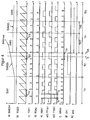
- Figure 4 shows a) the time course of the load current setpoints, b) the output voltage of the timing element of the clock generator TG, c) the voltage at the output TGA1 of the clock generator TG, d) the voltage at the output TGA2 of the clock generator TG, e) the voltage at the output ASA1 the output stage AS, e1) the voltage at the output TT1A1 of the driver TT1, e2) the voltage at the output TT2A1 of the driver TT2, f) the voltage at the output SRA1 of the current regulator circuit SR, g) the voltage at the output ZA1 of the counter Z, and h ) the voltage at the output ZA2 of the counter Z.
- the voltage curves mentioned are shown for the preheating phase TV, the ignition phase TZ with the ignition point t Z , the start-up phase TA and for normal operation TN.
- SW1 increases until the ignition is recognized (time t ZE ).
- SW3 is formed in period TA1.
- the setpoint SW4 (t) is formed in the period TA2 as a function of the analog signals formed by DAW.
- the setpoint SW5 is formed in the period TN.
- FIG. 4b shows the profile of the output voltage of the timing element of the clock generator TG.
- the clock generator works in free-running mode with the period t TG .
- the timer becomes the first and every further occurrence of a signal at the output SRA1 of the current regulator SR set in its initial state and thereby synchronized with the frequency f Inv of the inverter. If no signal occurs at the output SRA1 due to the ignition of the lamp within the period t TG , the ignition of the lamp which occurred at the time t Z is thus recognized and the ignition phase is ended.
- FIG. 4c shows the signals at the output TGA1 of the clock generator TG.
- a switching pulse occurs whenever the timing element of the clock generator is set to its initial state (FIG. 4b).
- the frequency of the switching pulses at TGA1 corresponds to the inverter frequency f Inv (synchronized operation), except for the ignition phase of the frequency f TG of the free-running clock generator.
- FIG. 4d shows the signals at the output TGA2 of the clock generator TG.
- a switching pulse only occurs when the timing element of the clock generator is set to its initial state by the feedback network at the end of its period t TG (FIG. 4b). No switching pulses occur during the ignition phase TZ, as long as the timer is reset by the signals at the input TGE1 before the period t TG has expired.
- Figure 4e shows the output signal ASA1 of the output stage AS.
- the two half-bridge switching elements T1, T2 are activated.
- a dead time t T begins, after which the previously inactive switching element is activated.
- FIG. 4f shows the signals at the output SRA1 of the current regulator circuit SR.
- a switching pulse always occurs when the detected actual current time area becomes larger than the specified target current time area.
- the switching pulses cause a change in state of the output stage AS or the signal ASA1 (FIG. 4e).
- no switching pulse occurs at the output SRA1 within a period t TG of the clock generator TG.
- Figure 4g shows the output signal ZA1 of the counter Z, which indicates the ignition phase TZ, for example by a signal "1".
- Figure 4h shows the output signal ZA2 of the counter Z, which indicates the burning of the lamp EL (start-up phase TA and normal operating phase TN), for example by a signal "1".
Landscapes
- Circuit Arrangements For Discharge Lamps (AREA)
Applications Claiming Priority (2)
| Application Number | Priority Date | Filing Date | Title |
|---|---|---|---|
| DE19546588 | 1995-12-13 | ||
| DE19546588A DE19546588A1 (de) | 1995-12-13 | 1995-12-13 | Verfahren und Schaltungsanordnung zum Betrieb einer Entladungslampe |
Publications (3)
| Publication Number | Publication Date |
|---|---|
| EP0779768A2 true EP0779768A2 (fr) | 1997-06-18 |
| EP0779768A3 EP0779768A3 (fr) | 1997-10-29 |
| EP0779768B1 EP0779768B1 (fr) | 2000-05-10 |
Family
ID=7780047
Family Applications (1)
| Application Number | Title | Priority Date | Filing Date |
|---|---|---|---|
| EP96118851A Expired - Lifetime EP0779768B1 (fr) | 1995-12-13 | 1996-11-25 | Circuit pour alimenter une lampe à décharge |
Country Status (7)
| Country | Link |
|---|---|
| US (1) | US5828187A (fr) |
| EP (1) | EP0779768B1 (fr) |
| JP (1) | JPH09219293A (fr) |
| KR (1) | KR100432541B1 (fr) |
| CN (1) | CN1199525C (fr) |
| CA (1) | CA2192506C (fr) |
| DE (2) | DE19546588A1 (fr) |
Cited By (2)
| Publication number | Priority date | Publication date | Assignee | Title |
|---|---|---|---|---|
| WO2008138391A1 (fr) * | 2007-05-10 | 2008-11-20 | Osram Gesellschaft mit beschränkter Haftung | Circuit et procédé permettant de faire fonctionner au moins une lampe à décharge |
| WO2009092447A2 (fr) | 2008-01-24 | 2009-07-30 | Osram Gesellschaft mit beschränkter Haftung | Dispositif de circuit et procédé de réglage du courant au moyen d'au moins une lampe à décharge |
Families Citing this family (32)
| Publication number | Priority date | Publication date | Assignee | Title |
|---|---|---|---|---|
| JP3600976B2 (ja) * | 1998-07-14 | 2004-12-15 | 三菱電機株式会社 | 放電灯点灯装置 |
| DE19838830A1 (de) * | 1998-08-26 | 2000-03-02 | Patent Treuhand Ges Fuer Elektrische Gluehlampen Mbh | Verbesserte Anlaufschaltung für Niederdruck-Entladungslampe |
| US6963178B1 (en) * | 1998-12-07 | 2005-11-08 | Systel Development And Industries Ltd. | Apparatus for controlling operation of gas discharge devices |
| US6084362A (en) * | 1999-01-19 | 2000-07-04 | Chao; Wen-Shin | Electronic ballast capable of linear and stepless light regulation |
| JP3520795B2 (ja) * | 1999-02-15 | 2004-04-19 | 松下電工株式会社 | 放電灯点灯装置 |
| US7592753B2 (en) * | 1999-06-21 | 2009-09-22 | Access Business Group International Llc | Inductively-powered gas discharge lamp circuit |
| GB2353150A (en) * | 1999-08-03 | 2001-02-14 | Excil Electronics Ltd | Fluorescent lamp driver unit |
| US6198226B1 (en) * | 1999-08-18 | 2001-03-06 | Astronics Corporation | Low-noise drive circuit for electroluminescent lamp, and electroluminescent lamp assembly comprising same |
| JP2003522396A (ja) * | 2000-02-10 | 2003-07-22 | コーニンクレッカ フィリップス エレクトロニクス エヌ ヴィ | Ntc抵抗を有する保護回路 |
| JP3322261B2 (ja) * | 2000-03-27 | 2002-09-09 | 松下電器産業株式会社 | 放電ランプ点灯装置 |
| JP3975653B2 (ja) * | 2000-06-12 | 2007-09-12 | 松下電工株式会社 | 放電灯点灯装置 |
| DE10102837A1 (de) * | 2001-01-22 | 2002-07-25 | Patent Treuhand Ges Fuer Elektrische Gluehlampen Mbh | Betriebsgerät für Gasentladungslampen mit Abschaltung der Wendelheizung |
| DE10102940A1 (de) * | 2001-01-23 | 2002-08-08 | Patent Treuhand Ges Fuer Elektrische Gluehlampen Mbh | Mikrocontroller, Schaltnetzteil, Vorschaltgerät zum Betrieb mindestens einer elektrischen Lampe und Verfahren zum Betreiben mindestens einer elektrischen Lampe |
| US6628093B2 (en) * | 2001-04-06 | 2003-09-30 | Carlile R. Stevens | Power inverter for driving alternating current loads |
| DE10133515A1 (de) * | 2001-07-10 | 2003-01-30 | Patent Treuhand Ges Fuer Elektrische Gluehlampen Mbh | Schaltungsanordnung zum Betreiben einer Leuchtstofflampe |
| AU2003275281A1 (en) * | 2002-09-25 | 2004-04-19 | Lumitronics, Inc. | Circuit for driving cold cathode tubes |
| US20040227476A1 (en) * | 2002-12-19 | 2004-11-18 | International Rectifier Corp. | Flexible inverter power module for motor drives |
| JP2005166288A (ja) * | 2003-11-28 | 2005-06-23 | Mitsubishi Electric Corp | 放電灯点灯装置 |
| TWI258322B (en) * | 2003-12-17 | 2006-07-11 | Toshiba Lighting & Technology | Lighting apparatus for discharge lamp and illumination appliance |
| WO2005112523A1 (fr) * | 2004-05-11 | 2005-11-24 | Design Rite Llc. | Circuit d'excitation de tubes a cathode froide et lampes fluorescentes a electrode exterieure |
| US7227317B2 (en) * | 2004-06-10 | 2007-06-05 | Atmel Corporation | Method and system for enhanced dimming resolution in a light ballast through use of multiple control frequencies |
| CN1989790A (zh) | 2004-07-21 | 2007-06-27 | 皇家飞利浦电子股份有限公司 | 在换流期间生成同步的灯驱动器 |
| US20070103089A1 (en) * | 2005-05-11 | 2007-05-10 | Gilbert Fregoso | Circuit for driving cold cathode tubes and external electrode fluorescent lamps |
| US7821208B2 (en) * | 2007-01-08 | 2010-10-26 | Access Business Group International Llc | Inductively-powered gas discharge lamp circuit |
| KR101394612B1 (ko) * | 2007-05-02 | 2014-05-14 | 페어차일드코리아반도체 주식회사 | 램프 안정기 회로 |
| US20090200953A1 (en) * | 2008-02-08 | 2009-08-13 | Ray James King | Methods and apparatus for a high power factor ballast having high efficiency during normal operation and during dimming |
| US20090256481A1 (en) * | 2008-04-11 | 2009-10-15 | Osram Sylvania Inc. | Stand alone lamp filament preheat circuit for ballast |
| DE102009019625B4 (de) * | 2009-04-30 | 2014-05-15 | Osram Gmbh | Verfahren zum Ermitteln eines Typs einer Gasentladungslampe und elektronisches Vorschaltgerät zum Betreiben von mindestens zwei unterschiedlichen Typen von Gasentladungslampen |
| CN101990351A (zh) * | 2009-08-05 | 2011-03-23 | 广闳科技股份有限公司 | 荧光灯预热控制装置及其方法 |
| KR101658210B1 (ko) * | 2010-02-19 | 2016-09-21 | 페어차일드코리아반도체 주식회사 | 예열 제어 장치, 이를 포함하는 램프 구동 장치및 예열 제어 방법 |
| US8963447B2 (en) * | 2013-03-04 | 2015-02-24 | Osram Sylvania Inc. | Ballast with current control circuit |
| CN110165653B (zh) * | 2019-05-17 | 2023-09-22 | 北京人民电器厂有限公司 | 一种tt、tn配电系统 |
Citations (1)
| Publication number | Priority date | Publication date | Assignee | Title |
|---|---|---|---|---|
| EP0185179B1 (fr) | 1984-11-16 | 1989-03-22 | Patent-Treuhand-Gesellschaft für elektrische Glühlampen mbH | Circuit d'allumage pour une lampe à décharge à basse pression |
Family Cites Families (13)
| Publication number | Priority date | Publication date | Assignee | Title |
|---|---|---|---|---|
| EP0059064B1 (fr) * | 1981-02-21 | 1985-10-02 | THORN EMI plc | Circuit de démarrage et d'exploitation de lampes |
| AU2708684A (en) * | 1983-05-05 | 1984-11-08 | Dubank Electronics Pty. Ltd. | Electronic ballast and starter |
| EP0338109B1 (fr) * | 1988-04-20 | 1994-03-23 | Zumtobel Aktiengesellschaft | Convertisseur pour lampe à décharge |
| EP0359860A1 (fr) * | 1988-09-23 | 1990-03-28 | Siemens Aktiengesellschaft | Dispositif et procédé de mise en oeuvre d'au moins une lampe à décharge |
| DE69015418T2 (de) * | 1989-04-25 | 1995-05-04 | Matsushita Electric Works Ltd | Energieversorgung. |
| ATE123914T1 (de) * | 1989-07-10 | 1995-06-15 | Philips Electronics Na | Schaltungsanordnung. |
| US5048033A (en) * | 1990-09-04 | 1991-09-10 | Coherent, Inc. | Method and apparatus for controlling the power supply of a laser operating in a pulse mode |
| KR940001188B1 (ko) * | 1991-03-18 | 1994-02-16 | 조정환 | 고압 방전관용 전자식 안정화 장치 |
| US5128592A (en) * | 1991-07-18 | 1992-07-07 | Thomas Industries Inc. | High frequency ballast for gaseous discharge lamps |
| JP2772175B2 (ja) * | 1991-09-11 | 1998-07-02 | 株式会社テック | 放電灯点灯装置 |
| DE59409443D1 (de) * | 1994-04-15 | 2000-08-17 | Knobel Lichttech | Vorschaltgerät mit Lampenwechselerkennung für Entladungslampen |
| FR2721475B1 (fr) * | 1994-06-15 | 1996-07-19 | Sgs Thomson Microelectronics | Circuit de commande de commutation et dispositif de commande pour lampe fluorescente à basse pression. |
| TW266383B (en) * | 1994-07-19 | 1995-12-21 | Siemens Ag | Method of starting at least one fluorescent lamp by an electronic ballast and the electronic ballast used therefor |
-
1995
- 1995-12-13 DE DE19546588A patent/DE19546588A1/de not_active Withdrawn
-
1996
- 1996-11-25 DE DE59605182T patent/DE59605182D1/de not_active Expired - Lifetime
- 1996-11-25 EP EP96118851A patent/EP0779768B1/fr not_active Expired - Lifetime
- 1996-12-10 CA CA002192506A patent/CA2192506C/fr not_active Expired - Fee Related
- 1996-12-11 JP JP8346488A patent/JPH09219293A/ja active Pending
- 1996-12-12 US US08/764,491 patent/US5828187A/en not_active Expired - Lifetime
- 1996-12-13 CN CNB961215208A patent/CN1199525C/zh not_active Expired - Fee Related
- 1996-12-13 KR KR1019960065033A patent/KR100432541B1/ko not_active Expired - Fee Related
Patent Citations (1)
| Publication number | Priority date | Publication date | Assignee | Title |
|---|---|---|---|---|
| EP0185179B1 (fr) | 1984-11-16 | 1989-03-22 | Patent-Treuhand-Gesellschaft für elektrische Glühlampen mbH | Circuit d'allumage pour une lampe à décharge à basse pression |
Cited By (5)
| Publication number | Priority date | Publication date | Assignee | Title |
|---|---|---|---|---|
| WO2008138391A1 (fr) * | 2007-05-10 | 2008-11-20 | Osram Gesellschaft mit beschränkter Haftung | Circuit et procédé permettant de faire fonctionner au moins une lampe à décharge |
| CN101682971B (zh) * | 2007-05-10 | 2013-05-15 | 奥斯兰姆有限公司 | 用于驱动至少一个放电灯的电路装置和方法 |
| WO2009092447A2 (fr) | 2008-01-24 | 2009-07-30 | Osram Gesellschaft mit beschränkter Haftung | Dispositif de circuit et procédé de réglage du courant au moyen d'au moins une lampe à décharge |
| WO2009092447A3 (fr) * | 2008-01-24 | 2010-04-22 | Osram Gesellschaft mit beschränkter Haftung | Dispositif de circuit et procédé de réglage du courant au moyen d'au moins une lampe à décharge |
| US8207681B2 (en) | 2008-01-24 | 2012-06-26 | Osram Ag | Circuit arrangement and method for regulating the current through at least one discharge lamp |
Also Published As
| Publication number | Publication date |
|---|---|
| CN1199525C (zh) | 2005-04-27 |
| KR970058386A (ko) | 1997-07-31 |
| EP0779768A3 (fr) | 1997-10-29 |
| US5828187A (en) | 1998-10-27 |
| KR100432541B1 (ko) | 2004-08-11 |
| CA2192506C (fr) | 2004-11-16 |
| CN1155825A (zh) | 1997-07-30 |
| DE59605182D1 (de) | 2000-06-15 |
| EP0779768B1 (fr) | 2000-05-10 |
| CA2192506A1 (fr) | 1997-06-14 |
| JPH09219293A (ja) | 1997-08-19 |
| DE19546588A1 (de) | 1997-06-19 |
Similar Documents
| Publication | Publication Date | Title |
|---|---|---|
| EP0779768B1 (fr) | Circuit pour alimenter une lampe à décharge | |
| EP1103165B1 (fr) | Ballast electronique destine a au moins une lampe a decharge basse tension | |
| EP1227707B1 (fr) | Microcontrôleur, alimentation à découpage et ballast électronique pour la mise en oeuvre d'au moins une lampe | |
| DE68918034T2 (de) | Leistungssteuerschaltung für Gasentladungslampen und Verfahren für den Betrieb. | |
| EP1333707B1 (fr) | Ballast électronique pour une lampe à décharge | |
| EP1519638B1 (fr) | Méthode pour commander une lampe à décharge basse pression | |
| DE10025610B4 (de) | Ansteuergerät für eine Entladungslampe | |
| EP0338109B1 (fr) | Convertisseur pour lampe à décharge | |
| EP0359860A1 (fr) | Dispositif et procédé de mise en oeuvre d'au moins une lampe à décharge | |
| DE4017415C2 (de) | Schaltungsanordnung zum Betrieb einer Hochdruck-Entladungslampe für einen Fahrzeugscheinwerfer | |
| EP0800335B1 (fr) | Circuit pour alimenter des lampes électriques | |
| EP0707438A2 (fr) | Ballast pour au moins une lampe à décharge | |
| DE60205830T2 (de) | Vorschaltgerät mit effizienter Elektroden-Vorheizung und Lampenfehlerschutz | |
| DE102006061357B4 (de) | Verfahren zur Ansteuerung einer Leuchtstofflampe | |
| EP0264765A2 (fr) | Disposition de circuit pour la mise en oeuvre de lampe à incandescence halogène basse tension | |
| EP1705961A2 (fr) | Circuit et méthode pour alimenter des lampes | |
| DE69911493T2 (de) | Beleuchtungssystem einer Entladungslampe mit Überstromschutz für die Schalter eines Wechselrichters | |
| DE19626101A1 (de) | Beleuchtungsgerät mit Entladungslampe | |
| WO1998048597A1 (fr) | Circuiterie pour fonctionnement modulable d'un tube fluorescent | |
| DE10102339B4 (de) | Entladungslampen-Leuchtbetriebsschaltung | |
| DE3338464A1 (de) | Hochfrequenz-helligkeitssteuerung fuer leuchtstofflampen | |
| EP1276355B1 (fr) | Circuit ballast pour determiner la puissance de préchauffage | |
| EP0862844A1 (fr) | Transformateur electronique | |
| DE102004037389C5 (de) | Verfahren zur Ansteuerung einer eine Leuchtstofflampe aufweisenden Last zur Optimierung des Zündvorganges | |
| DE3511661A1 (de) | Vorschaltgeraet fuer gasentladungslampen |
Legal Events
| Date | Code | Title | Description |
|---|---|---|---|
| PUAI | Public reference made under article 153(3) epc to a published international application that has entered the european phase |
Free format text: ORIGINAL CODE: 0009012 |
|
| AK | Designated contracting states |
Kind code of ref document: A2 Designated state(s): BE DE FR GB IT NL |
|
| PUAL | Search report despatched |
Free format text: ORIGINAL CODE: 0009013 |
|
| AK | Designated contracting states |
Kind code of ref document: A3 Designated state(s): BE DE FR GB IT NL |
|
| 17P | Request for examination filed |
Effective date: 19971120 |
|
| 17Q | First examination report despatched |
Effective date: 19980120 |
|
| GRAG | Despatch of communication of intention to grant |
Free format text: ORIGINAL CODE: EPIDOS AGRA |
|
| GRAG | Despatch of communication of intention to grant |
Free format text: ORIGINAL CODE: EPIDOS AGRA |
|
| GRAH | Despatch of communication of intention to grant a patent |
Free format text: ORIGINAL CODE: EPIDOS IGRA |
|
| GRAH | Despatch of communication of intention to grant a patent |
Free format text: ORIGINAL CODE: EPIDOS IGRA |
|
| GRAA | (expected) grant |
Free format text: ORIGINAL CODE: 0009210 |
|
| AK | Designated contracting states |
Kind code of ref document: B1 Designated state(s): BE DE FR GB IT NL |
|
| RIC1 | Information provided on ipc code assigned before grant |
Free format text: 7H 05B 41/295 A |
|
| REF | Corresponds to: |
Ref document number: 59605182 Country of ref document: DE Date of ref document: 20000615 |
|
| ITF | It: translation for a ep patent filed | ||
| GBT | Gb: translation of ep patent filed (gb section 77(6)(a)/1977) |
Effective date: 20000714 |
|
| ET | Fr: translation filed | ||
| PLBE | No opposition filed within time limit |
Free format text: ORIGINAL CODE: 0009261 |
|
| STAA | Information on the status of an ep patent application or granted ep patent |
Free format text: STATUS: NO OPPOSITION FILED WITHIN TIME LIMIT |
|
| 26N | No opposition filed | ||
| REG | Reference to a national code |
Ref country code: GB Ref legal event code: IF02 |
|
| PGFP | Annual fee paid to national office [announced via postgrant information from national office to epo] |
Ref country code: GB Payment date: 20051108 Year of fee payment: 10 |
|
| PGFP | Annual fee paid to national office [announced via postgrant information from national office to epo] |
Ref country code: NL Payment date: 20051109 Year of fee payment: 10 |
|
| PGFP | Annual fee paid to national office [announced via postgrant information from national office to epo] |
Ref country code: BE Payment date: 20051118 Year of fee payment: 10 |
|
| PGFP | Annual fee paid to national office [announced via postgrant information from national office to epo] |
Ref country code: FR Payment date: 20051122 Year of fee payment: 10 |
|
| PG25 | Lapsed in a contracting state [announced via postgrant information from national office to epo] |
Ref country code: BE Free format text: LAPSE BECAUSE OF NON-PAYMENT OF DUE FEES Effective date: 20061130 |
|
| PG25 | Lapsed in a contracting state [announced via postgrant information from national office to epo] |
Ref country code: NL Free format text: LAPSE BECAUSE OF NON-PAYMENT OF DUE FEES Effective date: 20070601 |
|
| GBPC | Gb: european patent ceased through non-payment of renewal fee |
Effective date: 20061125 |
|
| NLV4 | Nl: lapsed or anulled due to non-payment of the annual fee |
Effective date: 20070601 |
|
| REG | Reference to a national code |
Ref country code: FR Ref legal event code: ST Effective date: 20070731 |
|
| PG25 | Lapsed in a contracting state [announced via postgrant information from national office to epo] |
Ref country code: GB Free format text: LAPSE BECAUSE OF NON-PAYMENT OF DUE FEES Effective date: 20061125 |
|
| BERE | Be: lapsed |
Owner name: *PATENT-TREUHAND-G.- FUR ELEKTRISCHE GLUHLAMPEN M. Effective date: 20061130 |
|
| PG25 | Lapsed in a contracting state [announced via postgrant information from national office to epo] |
Ref country code: FR Free format text: LAPSE BECAUSE OF NON-PAYMENT OF DUE FEES Effective date: 20061130 |
|
| REG | Reference to a national code |
Ref country code: DE Ref legal event code: R081 Ref document number: 59605182 Country of ref document: DE Owner name: OSRAM GMBH, DE Free format text: FORMER OWNER: OSRAM GESELLSCHAFT MIT BESCHRAENKTER HAFTUNG, 81543 MUENCHEN, DE Effective date: 20111130 |
|
| PGFP | Annual fee paid to national office [announced via postgrant information from national office to epo] |
Ref country code: IT Payment date: 20121123 Year of fee payment: 17 |
|
| REG | Reference to a national code |
Ref country code: DE Ref legal event code: R081 Ref document number: 59605182 Country of ref document: DE Owner name: OSRAM GMBH, DE Free format text: FORMER OWNER: OSRAM AG, 81543 MUENCHEN, DE Effective date: 20130205 |
|
| REG | Reference to a national code |
Ref country code: DE Ref legal event code: R081 Ref document number: 59605182 Country of ref document: DE Owner name: OSRAM GMBH, DE Free format text: FORMER OWNER: OSRAM GMBH, 81543 MUENCHEN, DE Effective date: 20130822 |
|
| PG25 | Lapsed in a contracting state [announced via postgrant information from national office to epo] |
Ref country code: IT Free format text: LAPSE BECAUSE OF NON-PAYMENT OF DUE FEES Effective date: 20131125 |
|
| PGFP | Annual fee paid to national office [announced via postgrant information from national office to epo] |
Ref country code: DE Payment date: 20141119 Year of fee payment: 19 |
|
| REG | Reference to a national code |
Ref country code: DE Ref legal event code: R119 Ref document number: 59605182 Country of ref document: DE |
|
| PG25 | Lapsed in a contracting state [announced via postgrant information from national office to epo] |
Ref country code: DE Free format text: LAPSE BECAUSE OF NON-PAYMENT OF DUE FEES Effective date: 20160601 |