EP0782278A2 - Procédé pour le traitement d'un signal - Google Patents
Procédé pour le traitement d'un signal Download PDFInfo
- Publication number
- EP0782278A2 EP0782278A2 EP96119957A EP96119957A EP0782278A2 EP 0782278 A2 EP0782278 A2 EP 0782278A2 EP 96119957 A EP96119957 A EP 96119957A EP 96119957 A EP96119957 A EP 96119957A EP 0782278 A2 EP0782278 A2 EP 0782278A2
- Authority
- EP
- European Patent Office
- Prior art keywords
- signal
- input signal
- input
- guardband
- stored value
- Prior art date
- Legal status (The legal status is an assumption and is not a legal conclusion. Google has not performed a legal analysis and makes no representation as to the accuracy of the status listed.)
- Granted
Links
Images

Classifications
-
- H—ELECTRICITY
- H04—ELECTRIC COMMUNICATION TECHNIQUE
- H04B—TRANSMISSION
- H04B10/00—Transmission systems employing electromagnetic waves other than radio-waves, e.g. infrared, visible or ultraviolet light, or employing corpuscular radiation, e.g. quantum communication
-
- H—ELECTRICITY
- H04—ELECTRIC COMMUNICATION TECHNIQUE
- H04B—TRANSMISSION
- H04B10/00—Transmission systems employing electromagnetic waves other than radio-waves, e.g. infrared, visible or ultraviolet light, or employing corpuscular radiation, e.g. quantum communication
- H04B10/60—Receivers
- H04B10/66—Non-coherent receivers, e.g. using direct detection
- H04B10/69—Electrical arrangements in the receiver
- H04B10/697—Arrangements for reducing noise and distortion
-
- H—ELECTRICITY
- H04—ELECTRIC COMMUNICATION TECHNIQUE
- H04L—TRANSMISSION OF DIGITAL INFORMATION, e.g. TELEGRAPHIC COMMUNICATION
- H04L25/00—Baseband systems
- H04L25/02—Details ; arrangements for supplying electrical power along data transmission lines
- H04L25/06—DC level restoring means; Bias distortion correction ; Decision circuits providing symbol by symbol detection
- H04L25/061—DC level restoring means; Bias distortion correction ; Decision circuits providing symbol by symbol detection providing hard decisions only; arrangements for tracking or suppressing unwanted low frequency components, e.g. removal of DC offset
- H04L25/062—Setting decision thresholds using feedforward techniques only
Definitions
- the present invention relates, in general, to communication systems, and more particularly, to signal processing circuits for communication systems.
- One problem with the adaptive feedback receivers is the operation during idle time of the burst-mode communication signal applied to the receiver.
- Such circuits typically utilize differential amplifiers and have feedback loops in order to implement automatic gain control and automatic offset control within the receivers.
- the feedback loop decreases threshold voltage applied to the differential amplifiers thereby causing the receiver to output noise.
- the peak and minimum input voltage values drift over time causing pulse width distortion or even erroneous signals in the output from the receivers.
- FIG. 1 schematically illustrates a signal processing circuit 10 that is suitable for receiving burst-mode signals, and that minimizes pulse-width distortion.
- Circuit 10 includes a received data input 11 suitable for accepting a received signal, such as the signal from a photodetector 12 that detects light received by a fiber optic communication system.
- the received signal on input 11 is applied to an input of preamplifier 13 which amplifies the received signal and forms an input signal on an output of preamplifier 13.
- the input signal is applied to a signal input 14 of circuit 10.
- a sample and hold circuit 16 receives the input signal from input 14 and stores a maximum stored value of the input signal on a storage element that is part of circuit 16. This function is typically referred to as sampling the input signal and holding the maximum stored value of the input signal on the storage element.
- a reset signal is applied to a reset input 32 of circuit 16 in order to change the maximum value of the input signal that is stored on the storage element as will be seen hereinafter.
- the maximum stored value of the input signal is applied to an output 18 of circuit 16.
- a guardband circuit 19 receives the maximum stored value from output 18 and generates a guardband signal on an output 21 of circuit 19.
- the guardband signal is less than the maximum value of the input signal and is used to determine when the input signal amplitude has decreased to a value that requires resetting circuit 16 in order to change the maximum stored value of the input signal.
- the differential between the maximum stored value of the input signal and the guardband signal typically is chosen to be a multiple of the signal noise value on the input signal applied to input 14. That is, the guardband signal is less than the maximum stored value of the input signal by an amount that is a multiple of the noise anticipated on the input signal. This differential value differs based on the system environment in which signal processing circuit 10 is used.
- Guardband circuit 19 can have a variety of circuit implementations including a simple resistive voltage divider.
- the guardband signal is applied to a positive input of a comparator 22 while the input signal from input 14 is applied to a negative input of comparator 22.
- comparator 22 compares the input signal to the guardband signal.
- Comparator 22 produces a below guardband signal on an output 23.
- the below guardband signal is an inverted reproduction of the input signal as long as the maximum value of the input signal remains greater than the guardband signal.
- output 23 remains at a high voltage level. Setting the guardband signal less than the maximum value of the input signal by a multiple of the input noise assist in ensuring that noise on the input signal does not result in false indications that the input signal is below the guardband signal.
- a ratio circuit 24 receives the maximum stored value of the input signal and generates a threshold value or threshold signal on an output 25.
- the threshold signal is a percentage value of the maximum stored value of the input signal, that is, circuit 24 functions as a divider that reduces the value of the maximum stored value of the input signal by a percentage value.
- Circuit 24 can have a variety of circuit implementations including, but not limited to, a resistive voltage divider network.
- the threshold value or threshold signal is used to bias a comparator 26 and is compared to the input signal in order to reproduce the waveshape of the input signal. Consequently, output 25 is connected to a negative input of comparator 26 while the input signal is applied to a positive input of comparator 26.
- the waveshape of the input signal is reproduced on an output 27 of comparator 26.
- the percentage value is approximately fifty percent, that is, the threshold signal is approximately one-half of the maximum stored value of the input signal that is presented on output 18. This assists in ensuring that the output signal on output 27 is symmetrical and minimizing pulse width distortion.
- a logical AND circuit 28 is used to generate a recapture signal on an output 29 of circuit 28.
- Circuit 28 logically ANDs the output signal on output 27 with the below guardband signal on output 23.
- the recapture signal becomes active and subsequently causes circuit 16 to be reset . That is, when the input signal on input 14 is both greater than the threshold signal and less than the guardband signal, the recapture signal becomes active.
- circuit 28 performs a digital function, it typically is an analog circuit, as will be seen hereinafter in FIG. 2, in order to match the voltages on outputs 23 and 27.
- a shaping circuit 31 receives the recapture signal and generates a reset signal on an output that is connected to reset input 32 of circuit 16.
- circuit 31 is a comparator with the recapture signal connected to a positive input and a bias signal connected to a negative input
- the bias signal is generated by circuitry, not shown, that is sufficient to remove noise on the recapture signal applied to circuit 31.
- the reset signal developed by circuit 31 has a voltage value that is suitable for causing circuit 16 to sample the input signal and store a new maximum stored value on the storage element of circuit 16.
- FIG. 2 schematically illustrates an embodiment of circuit 28 shown in FIG. 1. Elements of FIG. 2 that have the same reference numbers as FIG. 1 are the same as the corresponding FIG. 1 elements.
- FIG. 2 illustrates an example of one embodiment that can be used for circuit 28 even though many other implementations are possible.
- Circuit 28 includes a first current mirror 36 and a second current mirror 37 that are used to establish substantially identical currents i 1 and i 2 that flow when inputs 23 and 27, respectively, are active.
- a reference leg 38 has a current source 39 that establishes a current flow i 3 through a resistor R c2 that is approximately 1.5 times current i 1 or current i 2 . The voltage resulting from current i 3 is applied to a negative input of a comparator 41.
- the voltage resulting from currents i 1 and i 2 is applied to a positive input of comparator 41.
- either input 23 or 27 is a low voltage
- either current i 1 or current i 2 flows through a resistor R c1 .
- This causes the voltage at the positive input of comparator 41 to be greater than the voltage at the negative terminal, thus output 29 is at a high voltage.
- both inputs 23 and 27 are at a high voltage
- currents i 1 and i 2 both flow through resistor R c1 and the voltage at the positive input of comparative 41 is less than the voltage at the negative input so that output 29 is at a low voltage.
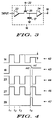
- FIG. 3 schematically illustrates an embodiment of a sample and hold circuit that is suitable for use as circuit 16 shown in FIG. 1. Elements of FIG. 3 that have the same reference numbers as FIG. 1 are the same as the corresponding FIG. 1 elements.
- FIG. 3 illustrates an example of one embodiment that can be used for circuit 16 even though many other implementations are possible.
- Circuit 16 includes an input buffer 33 that isolates circuit 16 from input 14.
- a switch 35 is used to couple the output of buffer 33 to a storage element 17 when the reset signal is applied to circuit 16.
- An output buffer 34 isolates storage element 17 from circuitry connected to output 18.
- storage element 17 is a capacitor as illustrated in FIG. 2.
- FIG. 4 is a timing diagram illustrating timing for the reset function of circuit 10. Elements of FIG. 4 that have the same reference numbers as FIG. 1, refer to the corresponding FIG. 1 elements.
- the input signal on input 14 of circuit 10 is illustrated by a waveform 42.
- a waveform 43 represents the maximum stored input value on output 18, a waveform 44 illustrates the below guardband signal on output 23, a waveform 46 illustrates the output signal on output 27, and a waveform 47 illustrates the recapture signal on output 29.
- the input signal becomes a positive voltage and a first maximum stored value m1 is applied to output 18. Because the input signal (waveform 42) is greater than the guardband signal the below guardband signal (waveform 44) becomes negative.
- the output signal (waveform 46) of circuit 10 goes high. Since the below guardband signal (waveform 44) is low, the recapture signal (waveform 47) from AND circuit 28 is at a low voltage.
- the input signal (waveform 42) goes low. Because this value of the input signal is less than the guardband signal, the below guardband signal (waveform 44) goes high. Because the input signal is below the threshold signal, the output signal (waveform 46) goes low and presents a low voltage to AND circuit 28, thus, the recapture signal (waveform 47) remains a low voltage.
- waveforms 44 and 46 once again present a low voltage to circuit 28 so that the recapture signal (waveform 47) remains low. This is similar to the sequence at time t 1 .
- the input signal (waveform 42) once again goes high but the maximum value of the input signal is now less than the maximum value during time t 1 and time t 3 . Because the value of the input signal at time t 4 is less than the guardband signal, the below guardband signal (waveform 44) remains high after time t 4 . Because the input signal is above the threshold signal the output signal on output 27 (waveform 46) goes high as indicated. Consequently, there is an overlap between the output signal and the below guardband signal at time t 4 so that both inputs 23 and 27 of circuit 28 (waveforms 44 and 46, respectively) are high. This causes the recapture signal on output 29 (waveform 47) to go high at time t 4 .
- sample and hold circuit 16 changes the maximum stored value on the storage element to a second maximum value m2 (waveform 43) which is the new value of the input signal. Because the maximum stored value has changed to the new lower maximum value of the input signal, the input signal is now greater than the guardband signal and the below guardband signal goes low (waveform 44) causing the recapture signal (waveform 47) to go low and end the reset process. Therefore, a new maximum stored value has been acquired which changes the threshold signal applied to comparator 26 thereby ensuring that the threshold voltage applied to comparator 26 is the proper percentage of the maximum value of the input signal so that the output signal on output 27 substantially reproduces the input signal without pulse width distortion. It should be noted however that a small amount of pulse width distortion will exist in the first pulse out of circuit 10 after time t4. This is due to the rising edge of the input signal being compared to an improper threshold prior to the time circuit 16 is reset to change the maximum stored value.
- Comparing the input signal to a guardbanded value of the maximum input signal facilitates determining when the maximum value of the input signal has changed and a new threshold voltage should be utilized in order to reconstruct the input signal.
- Changing the maximum stored value of the input signal while the input signal is high facilitates storing the new maximum value of the input signal and also facilitates establishing a new threshold voltage substantially without introducing pulse width distortion. Because feedback circuits are not utilized for setting amplifier gains, the circuit does not oscillate.
Landscapes
- Engineering & Computer Science (AREA)
- Computer Networks & Wireless Communication (AREA)
- Signal Processing (AREA)
- Physics & Mathematics (AREA)
- Electromagnetism (AREA)
- Power Engineering (AREA)
- Dc Digital Transmission (AREA)
- Tone Control, Compression And Expansion, Limiting Amplitude (AREA)
- Manipulation Of Pulses (AREA)
- Noise Elimination (AREA)
Applications Claiming Priority (2)
| Application Number | Priority Date | Filing Date | Title |
|---|---|---|---|
| US578726 | 1995-12-26 | ||
| US08/578,726 US5703506A (en) | 1995-12-26 | 1995-12-26 | Signal processing method |
Publications (3)
| Publication Number | Publication Date |
|---|---|
| EP0782278A2 true EP0782278A2 (fr) | 1997-07-02 |
| EP0782278A3 EP0782278A3 (fr) | 1998-12-16 |
| EP0782278B1 EP0782278B1 (fr) | 2002-10-09 |
Family
ID=24314047
Family Applications (1)
| Application Number | Title | Priority Date | Filing Date |
|---|---|---|---|
| EP96119957A Expired - Lifetime EP0782278B1 (fr) | 1995-12-26 | 1996-12-12 | Procédé pour le traitement d'un signal |
Country Status (5)
| Country | Link |
|---|---|
| US (1) | US5703506A (fr) |
| EP (1) | EP0782278B1 (fr) |
| KR (1) | KR100436096B1 (fr) |
| DE (1) | DE69624211T2 (fr) |
| TW (1) | TW353248B (fr) |
Cited By (1)
| Publication number | Priority date | Publication date | Assignee | Title |
|---|---|---|---|---|
| EP1257103A1 (fr) * | 2001-05-11 | 2002-11-13 | Alcatel | Circuit pour déterminer les niveaux des flux de données |
Families Citing this family (22)
| Publication number | Priority date | Publication date | Assignee | Title |
|---|---|---|---|---|
| US6222762B1 (en) | 1992-01-14 | 2001-04-24 | Sandisk Corporation | Multi-state memory |
| US5657332A (en) | 1992-05-20 | 1997-08-12 | Sandisk Corporation | Soft errors handling in EEPROM devices |
| US5835413A (en) * | 1996-12-20 | 1998-11-10 | Intel Corporation | Method for improved data retention in a nonvolatile writeable memory by sensing and reprogramming cell voltage levels |
| US5909449A (en) * | 1997-09-08 | 1999-06-01 | Invox Technology | Multibit-per-cell non-volatile memory with error detection and correction |
| US7173852B2 (en) | 2003-10-03 | 2007-02-06 | Sandisk Corporation | Corrected data storage and handling methods |
| US7012835B2 (en) | 2003-10-03 | 2006-03-14 | Sandisk Corporation | Flash memory data correction and scrub techniques |
| US7395404B2 (en) * | 2004-12-16 | 2008-07-01 | Sandisk Corporation | Cluster auto-alignment for storing addressable data packets in a non-volatile memory array |
| US7315916B2 (en) | 2004-12-16 | 2008-01-01 | Sandisk Corporation | Scratch pad block |
| US7423458B2 (en) * | 2006-03-08 | 2008-09-09 | Analog Devices, Inc. | Multiple sampling sample and hold architectures |
| US7716538B2 (en) | 2006-09-27 | 2010-05-11 | Sandisk Corporation | Memory with cell population distribution assisted read margining |
| US7886204B2 (en) | 2006-09-27 | 2011-02-08 | Sandisk Corporation | Methods of cell population distribution assisted read margining |
| US7477547B2 (en) * | 2007-03-28 | 2009-01-13 | Sandisk Corporation | Flash memory refresh techniques triggered by controlled scrub data reads |
| US7573773B2 (en) | 2007-03-28 | 2009-08-11 | Sandisk Corporation | Flash memory with data refresh triggered by controlled scrub data reads |
| US8687421B2 (en) | 2011-11-21 | 2014-04-01 | Sandisk Technologies Inc. | Scrub techniques for use with dynamic read |
| US9230689B2 (en) | 2014-03-17 | 2016-01-05 | Sandisk Technologies Inc. | Finding read disturbs on non-volatile memories |
| US9552171B2 (en) | 2014-10-29 | 2017-01-24 | Sandisk Technologies Llc | Read scrub with adaptive counter management |
| US9978456B2 (en) | 2014-11-17 | 2018-05-22 | Sandisk Technologies Llc | Techniques for reducing read disturb in partially written blocks of non-volatile memory |
| US9349479B1 (en) | 2014-11-18 | 2016-05-24 | Sandisk Technologies Inc. | Boundary word line operation in nonvolatile memory |
| US9449700B2 (en) | 2015-02-13 | 2016-09-20 | Sandisk Technologies Llc | Boundary word line search and open block read methods with reduced read disturb |
| US9653154B2 (en) | 2015-09-21 | 2017-05-16 | Sandisk Technologies Llc | Write abort detection for multi-state memories |
| US9997254B2 (en) | 2016-07-13 | 2018-06-12 | Nxp Usa, Inc. | Sample-and-hold circuit |
| US9984763B1 (en) * | 2016-11-30 | 2018-05-29 | Nxp Usa, Inc. | Sample and hold circuit |
Family Cites Families (8)
| Publication number | Priority date | Publication date | Assignee | Title |
|---|---|---|---|---|
| US3599105A (en) * | 1969-07-24 | 1971-08-10 | Hughes Aircraft Co | Amplitude discriminator with an adaptive threshold |
| GB1343694A (en) * | 1971-05-13 | 1974-01-16 | Nat Res Dev | Stress wave emission defect location system |
| US4241455A (en) * | 1977-12-29 | 1980-12-23 | Sperry Corporation | Data receiving and processing circuit |
| US4276539A (en) * | 1978-06-22 | 1981-06-30 | U.S. Philips Corporation | Vehicle detection systems |
| JPS60205865A (ja) * | 1984-03-30 | 1985-10-17 | Pioneer Electronic Corp | 波形整形回路 |
| JPH0375976A (ja) * | 1989-08-18 | 1991-03-29 | Fujitsu Ltd | 半導体集積回路装置 |
| US5434564A (en) * | 1991-09-30 | 1995-07-18 | Koga Electronics Co., Ltd. | Method and apparatus for producing pulses corresponding in number to the amount of changes in a physicial quantity |
| KR100339347B1 (ko) * | 1995-02-13 | 2002-11-30 | 엘지전자주식회사 | 디브이씨알(dvcr)의데이타복원장치 |
-
1995
- 1995-12-26 US US08/578,726 patent/US5703506A/en not_active Expired - Fee Related
-
1996
- 1996-08-29 TW TW085110530A patent/TW353248B/zh active
- 1996-12-12 DE DE69624211T patent/DE69624211T2/de not_active Expired - Fee Related
- 1996-12-12 EP EP96119957A patent/EP0782278B1/fr not_active Expired - Lifetime
- 1996-12-23 KR KR1019960070035A patent/KR100436096B1/ko not_active Expired - Fee Related
Non-Patent Citations (1)
| Title |
|---|
| None |
Cited By (1)
| Publication number | Priority date | Publication date | Assignee | Title |
|---|---|---|---|---|
| EP1257103A1 (fr) * | 2001-05-11 | 2002-11-13 | Alcatel | Circuit pour déterminer les niveaux des flux de données |
Also Published As
| Publication number | Publication date |
|---|---|
| KR100436096B1 (ko) | 2004-08-18 |
| DE69624211T2 (de) | 2003-02-13 |
| US5703506A (en) | 1997-12-30 |
| DE69624211D1 (de) | 2002-11-14 |
| EP0782278A3 (fr) | 1998-12-16 |
| KR970056064A (ko) | 1997-07-31 |
| EP0782278B1 (fr) | 2002-10-09 |
| TW353248B (en) | 1999-02-21 |
Similar Documents
| Publication | Publication Date | Title |
|---|---|---|
| US5703506A (en) | Signal processing method | |
| EP0611059B1 (fr) | Système pour récupérer une composante de courant continu pour les signaux binaires transférés en série | |
| US4385328A (en) | Data extracting circuit | |
| US4375037A (en) | Receiving circuit | |
| JPH10163828A (ja) | レベル識別回路 | |
| US4063183A (en) | Adaptive equalizer with improved distortion analysis | |
| US4994692A (en) | Quantizer system | |
| US4423518A (en) | Timing recovery circuit | |
| JP2962218B2 (ja) | ディジタル光受信回路 | |
| US5969547A (en) | Analog signal processing circuit with noise immunity and reduced delay | |
| JP2000156630A (ja) | 自動識別レベル制御回路 | |
| US6215334B1 (en) | Analog signal processing circuit with noise immunity and reduced delay | |
| JPH11168335A (ja) | 利得制御機能付受信装置 | |
| JP3064703B2 (ja) | サンプルホールド回路 | |
| JPH01286655A (ja) | 光受信回路 | |
| JPH04223789A (ja) | 信号スロープ急峻化回路配置 | |
| EP0782263A1 (fr) | Détecteur de flancs avec hystéresis | |
| EP1322082A1 (fr) | Circuit de la tension de polarisation continue pour un récepteur optique | |
| EP0782264A2 (fr) | Récepteur numérique à seuils adaptifs | |
| US5703504A (en) | Feedforward adaptive threshold processing method | |
| JP2000022765A (ja) | Atc機能付受信装置 | |
| JPH0413280A (ja) | 記録情報再生用フェーズドロックループ回路 | |
| JP2834461B2 (ja) | 波形整形回路 | |
| JPS6369336A (ja) | 光受信回路 | |
| JPS63248256A (ja) | バ−ストデ−タ用光受信回路 |
Legal Events
| Date | Code | Title | Description |
|---|---|---|---|
| PUAI | Public reference made under article 153(3) epc to a published international application that has entered the european phase |
Free format text: ORIGINAL CODE: 0009012 |
|
| AK | Designated contracting states |
Kind code of ref document: A2 Designated state(s): DE FR GB |
|
| PUAL | Search report despatched |
Free format text: ORIGINAL CODE: 0009013 |
|
| RHK1 | Main classification (correction) |
Ipc: H03K 5/08 |
|
| AK | Designated contracting states |
Kind code of ref document: A3 Designated state(s): DE FR GB |
|
| 17P | Request for examination filed |
Effective date: 19990616 |
|
| 17Q | First examination report despatched |
Effective date: 20010206 |
|
| GRAG | Despatch of communication of intention to grant |
Free format text: ORIGINAL CODE: EPIDOS AGRA |
|
| GRAG | Despatch of communication of intention to grant |
Free format text: ORIGINAL CODE: EPIDOS AGRA |
|
| GRAH | Despatch of communication of intention to grant a patent |
Free format text: ORIGINAL CODE: EPIDOS IGRA |
|
| GRAH | Despatch of communication of intention to grant a patent |
Free format text: ORIGINAL CODE: EPIDOS IGRA |
|
| GRAA | (expected) grant |
Free format text: ORIGINAL CODE: 0009210 |
|
| AK | Designated contracting states |
Kind code of ref document: B1 Designated state(s): DE FR GB |
|
| REG | Reference to a national code |
Ref country code: GB Ref legal event code: FG4D |
|
| REF | Corresponds to: |
Ref document number: 69624211 Country of ref document: DE Date of ref document: 20021114 |
|
| PG25 | Lapsed in a contracting state [announced via postgrant information from national office to epo] |
Ref country code: GB Free format text: LAPSE BECAUSE OF NON-PAYMENT OF DUE FEES Effective date: 20030109 |
|
| ET | Fr: translation filed | ||
| PLBE | No opposition filed within time limit |
Free format text: ORIGINAL CODE: 0009261 |
|
| GBPC | Gb: european patent ceased through non-payment of renewal fee |
Effective date: 20030109 |
|
| 26N | No opposition filed |
Effective date: 20030710 |
|
| PGFP | Annual fee paid to national office [announced via postgrant information from national office to epo] |
Ref country code: FR Payment date: 20041201 Year of fee payment: 9 |
|
| PGFP | Annual fee paid to national office [announced via postgrant information from national office to epo] |
Ref country code: DE Payment date: 20041230 Year of fee payment: 9 |
|
| PG25 | Lapsed in a contracting state [announced via postgrant information from national office to epo] |
Ref country code: DE Free format text: LAPSE BECAUSE OF NON-PAYMENT OF DUE FEES Effective date: 20060701 |
|
| PG25 | Lapsed in a contracting state [announced via postgrant information from national office to epo] |
Ref country code: FR Free format text: LAPSE BECAUSE OF NON-PAYMENT OF DUE FEES Effective date: 20060831 |
|
| REG | Reference to a national code |
Ref country code: FR Ref legal event code: ST Effective date: 20060831 |