EP0786809A1 - Packung für elektronische Schaltung - Google Patents
Packung für elektronische Schaltung Download PDFInfo
- Publication number
- EP0786809A1 EP0786809A1 EP97100415A EP97100415A EP0786809A1 EP 0786809 A1 EP0786809 A1 EP 0786809A1 EP 97100415 A EP97100415 A EP 97100415A EP 97100415 A EP97100415 A EP 97100415A EP 0786809 A1 EP0786809 A1 EP 0786809A1
- Authority
- EP
- European Patent Office
- Prior art keywords
- wiring substrate
- data bus
- bus line
- chips
- electronic circuit
- Prior art date
- Legal status (The legal status is an assumption and is not a legal conclusion. Google has not performed a legal analysis and makes no representation as to the accuracy of the status listed.)
- Granted
Links
Images



Classifications
-
- G—PHYSICS
- G11—INFORMATION STORAGE
- G11C—STATIC STORES
- G11C5/00—Details of stores covered by group G11C11/00
- G11C5/02—Disposition of storage elements, e.g. in the form of a matrix array
- G11C5/04—Supports for storage elements, e.g. memory modules; Mounting or fixing of storage elements on such supports
-
- G—PHYSICS
- G11—INFORMATION STORAGE
- G11C—STATIC STORES
- G11C5/00—Details of stores covered by group G11C11/00
- G11C5/06—Arrangements for interconnecting storage elements electrically, e.g. by wiring
-
- H—ELECTRICITY
- H10—SEMICONDUCTOR DEVICES; ELECTRIC SOLID-STATE DEVICES NOT OTHERWISE PROVIDED FOR
- H10W—GENERIC PACKAGES, INTERCONNECTIONS, CONNECTORS OR OTHER CONSTRUCTIONAL DETAILS OF DEVICES COVERED BY CLASS H10
- H10W70/00—Package substrates; Interposers; Redistribution layers [RDL]
- H10W70/60—Insulating or insulated package substrates; Interposers; Redistribution layers
-
- H—ELECTRICITY
- H10—SEMICONDUCTOR DEVICES; ELECTRIC SOLID-STATE DEVICES NOT OTHERWISE PROVIDED FOR
- H10W—GENERIC PACKAGES, INTERCONNECTIONS, CONNECTORS OR OTHER CONSTRUCTIONAL DETAILS OF DEVICES COVERED BY CLASS H10
- H10W70/00—Package substrates; Interposers; Redistribution layers [RDL]
- H10W70/60—Insulating or insulated package substrates; Interposers; Redistribution layers
- H10W70/611—Insulating or insulated package substrates; Interposers; Redistribution layers for connecting multiple chips together
-
- H—ELECTRICITY
- H10—SEMICONDUCTOR DEVICES; ELECTRIC SOLID-STATE DEVICES NOT OTHERWISE PROVIDED FOR
- H10W—GENERIC PACKAGES, INTERCONNECTIONS, CONNECTORS OR OTHER CONSTRUCTIONAL DETAILS OF DEVICES COVERED BY CLASS H10
- H10W70/00—Package substrates; Interposers; Redistribution layers [RDL]
- H10W70/60—Insulating or insulated package substrates; Interposers; Redistribution layers
- H10W70/62—Insulating or insulated package substrates; Interposers; Redistribution layers characterised by their interconnections
- H10W70/65—Shapes or dispositions of interconnections
-
- H—ELECTRICITY
- H10—SEMICONDUCTOR DEVICES; ELECTRIC SOLID-STATE DEVICES NOT OTHERWISE PROVIDED FOR
- H10W—GENERIC PACKAGES, INTERCONNECTIONS, CONNECTORS OR OTHER CONSTRUCTIONAL DETAILS OF DEVICES COVERED BY CLASS H10
- H10W72/00—Interconnections or connectors in packages
-
- H—ELECTRICITY
- H10—SEMICONDUCTOR DEVICES; ELECTRIC SOLID-STATE DEVICES NOT OTHERWISE PROVIDED FOR
- H10W—GENERIC PACKAGES, INTERCONNECTIONS, CONNECTORS OR OTHER CONSTRUCTIONAL DETAILS OF DEVICES COVERED BY CLASS H10
- H10W90/00—Package configurations
-
- H—ELECTRICITY
- H10—SEMICONDUCTOR DEVICES; ELECTRIC SOLID-STATE DEVICES NOT OTHERWISE PROVIDED FOR
- H10W—GENERIC PACKAGES, INTERCONNECTIONS, CONNECTORS OR OTHER CONSTRUCTIONAL DETAILS OF DEVICES COVERED BY CLASS H10
- H10W70/00—Package substrates; Interposers; Redistribution layers [RDL]
- H10W70/60—Insulating or insulated package substrates; Interposers; Redistribution layers
- H10W70/62—Insulating or insulated package substrates; Interposers; Redistribution layers characterised by their interconnections
- H10W70/65—Shapes or dispositions of interconnections
- H10W70/654—Top-view layouts
- H10W70/656—Fan-in layouts
-
- H—ELECTRICITY
- H10—SEMICONDUCTOR DEVICES; ELECTRIC SOLID-STATE DEVICES NOT OTHERWISE PROVIDED FOR
- H10W—GENERIC PACKAGES, INTERCONNECTIONS, CONNECTORS OR OTHER CONSTRUCTIONAL DETAILS OF DEVICES COVERED BY CLASS H10
- H10W72/00—Interconnections or connectors in packages
- H10W72/071—Connecting or disconnecting
- H10W72/075—Connecting or disconnecting of bond wires
- H10W72/07551—Connecting or disconnecting of bond wires characterised by changes in properties of the bond wires during the connecting
- H10W72/07554—Connecting or disconnecting of bond wires characterised by changes in properties of the bond wires during the connecting changes in dispositions
-
- H—ELECTRICITY
- H10—SEMICONDUCTOR DEVICES; ELECTRIC SOLID-STATE DEVICES NOT OTHERWISE PROVIDED FOR
- H10W—GENERIC PACKAGES, INTERCONNECTIONS, CONNECTORS OR OTHER CONSTRUCTIONAL DETAILS OF DEVICES COVERED BY CLASS H10
- H10W72/00—Interconnections or connectors in packages
- H10W72/50—Bond wires
- H10W72/541—Dispositions of bond wires
- H10W72/547—Dispositions of multiple bond wires
-
- H—ELECTRICITY
- H10—SEMICONDUCTOR DEVICES; ELECTRIC SOLID-STATE DEVICES NOT OTHERWISE PROVIDED FOR
- H10W—GENERIC PACKAGES, INTERCONNECTIONS, CONNECTORS OR OTHER CONSTRUCTIONAL DETAILS OF DEVICES COVERED BY CLASS H10
- H10W72/00—Interconnections or connectors in packages
- H10W72/851—Dispositions of multiple connectors or interconnections
- H10W72/874—On different surfaces
- H10W72/884—Die-attach connectors and bond wires
-
- H—ELECTRICITY
- H10—SEMICONDUCTOR DEVICES; ELECTRIC SOLID-STATE DEVICES NOT OTHERWISE PROVIDED FOR
- H10W—GENERIC PACKAGES, INTERCONNECTIONS, CONNECTORS OR OTHER CONSTRUCTIONAL DETAILS OF DEVICES COVERED BY CLASS H10
- H10W90/00—Package configurations
- H10W90/701—Package configurations characterised by the relative positions of pads or connectors relative to package parts
- H10W90/751—Package configurations characterised by the relative positions of pads or connectors relative to package parts of bond wires
- H10W90/754—Package configurations characterised by the relative positions of pads or connectors relative to package parts of bond wires between a chip and a stacked insulating package substrate, interposer or RDL
Definitions
- the present invention relates to an electronic circuit package according to independent claims 1, 2, 11 and 13.
- a number of computers are being employed for various uses and a demand for smaller and lighter computers is also increased.
- Computers for use in space are required to be particularly smaller and lighter in order to decrease launching cost while increasing the payload.
- a checking unit for detecting errors and faults and a unit under check are accommodated in one and the same chip to reduce the size as described in "Trial Manufacture and Evaluation of Fault Tolerant Quartz Oscillation IC", by Tsuchimura et al, Research Material, 24th FTC Study Meeting.
- ASICs Application Specified ICs
- the object of the present invention is to provide a small and light electronic apparatus, in particular an electronic circuit package, with high reliability and in which the concentration of the wiring density is eased to prevent the increase of the package size.
- all semiconductor chips to be substantially connected by means of a bus line are bare chip packaged on a wiring substrate, and the semiconductor chips and the wiring substrate are connected by wiring bonding between wire bonding pads formed on the semiconductor chips and the wiring substrate.
- the wiring substrate may be a multilayer.
- an insulating layer partially formed on the surface of the multilayer wiring substrate and a die bonding ground formed on the surface of the insulating layer, in order to use a portion of the multilayer wiring substrate under the die bonding ground as a wiring or a via hole region, and at least one of the semiconductor chips is formed on the die bonding ground.
- the bus line includes two data bus lines.
- the semiconductor chips connected with one data bus line are formed on one side of the wiring substrate and the semiconductor chips connected with the other data bus line are formed on the other side of the wiring substrate.
- the semiconductor chips include a checking unit and a unit under check.
- Electronic apparatus as represented by computers are such that a plurality of semiconductor chips are normally connected to a bus having a number of signal lines.
- a bus having a number of signal lines.
- an enormous number of pins are required as the signal lines connected to the bus are used to couple the internal and external devices of a package.
- the present invention as all the semiconductor chips connected to the bus are formed into a single package, the number of signal lines connecting the inside and outside of the package is drastically reducible. In other words, the number of pins connecting between the signal lines inside and outside the wiring substrate decreases. As a result, electric apparatus become small and light.
- lead-out lines can be formed from wiring bonding pads and via holes even under the die bonding ground, according to the present invention, the wiring density in the neighborhood of the wire bonding pads is prevented from centering therearound. Therefore, the wiring density in each wiring layer is uniformized to the extent that they are effectively utilizable. As a result, the package becomes small.
- the data line connected to MIP Mocroprocessing Unit
- MIP Microprocessing Unit
- ROM Read Only Memory
- RAM Random Access Memory
- the data lines are grouped according to the width to be connected to the storage element and the storage element to be connected to the data line belonging to the same group is packaged on the same surface of the wiring substrate.
- the semiconductor element often causes transistor (gate)-based trouble in many cases, the trouble may involve the whole element (chip).
- the electronic apparatus comprising the checking unit and the unit under check is unable to detect the trouble, thus making the addition of the checking unit meaningless.
- the checking unit and the unit under check are separately provided in respective chips on the same wiring substrate on a bare chip basis.
- the wiring substrate and the bare chips are connected by wire bonding into a single package. The omission of a fault involving over the whole chip is thus prevented and furthermore, a small, light-weight electronic apparatus can be made available.
- Fig. 1 illustrates the inner construction of an electronic apparatus embodying the present invention by way of example.
- MPU 101, RAM 102, ROM 103, FPU (Floating-point Processing Unit) 104, DMAC (Direct Memory Access Controller) 105, and an interface circuit 106 are connected via a bus 100 in a wiring substrate 10.
- the bus 100 is not led out of the wiring substrate 10, but only an interface line 107 with external devices is led out of the wiring substrate 10.
- All semiconductor chips to be connected to the bus 100 are totally packaged on the wiring substrate 10 according to this embodiment.
- the bus 100 is not led out of the wiring substrate 10, the number of signal lines connecting between internal and external devices is reducible by a large margin. Accordingly, the number of pins connecting between the signal lines inside and outside the wiring substrate 10 decreases and this tides over an obstacle to rendering the wiring substrate smaller and lighter.
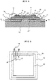
- Fig. 2 is a sectional view of a die bonding portion of the wiring substrate according to the present invention.
- Wire bonding pads 11 are formed on the wiring substrate 10 and an insulating layer 16 is formed on a wiring conductor 14 for use in leading out the wire bonding pad.
- a die bonding ground 15 is formed on the insulating layer 16 and a semiconductor chip 20 is bonded thereto by die bonding.
- a bonding wire 30 is then used for connecting between a wire bonding pad 21 on the semiconductor chip 20 and the wire bonding pad 11 on the wiring substrate 10.
- via holes 13, 13' may be formed in the periphery and inside of the die bonding ground 15, respectively.
- Said via hole 13 formed in the periphery of said die bonding ground 15 and said wire hole 13' formed inside of said die bonding ground 15 are preferably arranged alternately.
- a portion beneath the die bonding ground 15 as the outermost layer that has heretofore been unutilized may be put to practical use as a wiring and a via hole region.
- An area to be occupied by wiring and via hole regions can thus be made drastically smaller than what is occupied by the semiconductor chip of the wiring substrate.
- Fig. 4 refers to an embodiment wherein signal lines of the data bus 100 connected to MPU 101 are divided into two groups 100-1 and 100-2.
- RAMs 102-1 - 102-k and ROMs 103-1 - 103-k connected to the data bus 100-1 are packaged on one side (B side) of the substrate, whereas RAMS 102-(k+1) - 102-N, ROMs 103-(k+1) - 103-N connected to the data bus 100-2 are packaged on the other side (A side) of the substrate, wherein k and N is an integer.
- k and N is an integer.
- Fig. 5 refers to an embodiment, in case where the data bus 100 connected to the MPU 101 is 32 bits wide and the data bus connected to ROM and RAM is 8 bits wide.
- D0 - D31 constituting the data bus 100 D0 - D15 are formed into a group of data bus 100-1, and D16 - D31 into a group of data bus 100-2.
- D0 - D7 in the group of data bus 100-1 are connected to RAM 102-1 and ROM 103-1, and D8 - D15 to RAM 102-2 and ROM 103-2.
- D15 - D23 in the group of data bus 100-2 are connected to RAM 102-3 and ROM 103-3, and D24 - D31 to RAM 102-4 and ROM 103-4.
- the electronic apparatus can be made smaller and lighter as in the case of the embodiment shown in Fig. 4.
- Fig. 6 refers to an embodiment wherein MPU 101, a checking circuit 111 of the MPU 101, and RAM 102, an error correction code encoding/decoding circuit 112 are packaged in the form of bare chips on the wiring substrate 10. In this case, a bonding wire has been omitted for simplification.
- the MPU 101 and the checking circuit 111 are different bare chips and connected by wire bonding on the wiring substrate 10.
- various systems have been proposed as the checking circuit 111. There are the following, for instance:
- MPU 101 with the checking circuit 111 capable of detecting a fault involving the whole chip is provided without causing the number of packages and that of wires to increase. Therefore, a small lightweight, reliable electronic apparatus can be provided.
- RAM 102 and the error correction code encoding/decoding circuit 112 are different bare chips and connected by wire bonding on the wiring substrate 10.
- the error correction code adds an error detection/correction redundant bit to the data stored in the memory, thus causing an error to be detected and corrected by making a code-to-code Hamming distance 4 or greater.
- code-to-code Hamming distance When the code-to-code Hamming distance is set to 4, 1-bit error correction is possible, but a 2-bit error remains only detectable. Consequently, it is called SECDED (Single-Error-Correction, Double-Error Detection). For instance, a 6-bit detection/correction redundant bit needs adding when SECDED is meant to be realized concerning 16-bit data.
- SECDED Single-Error-Correction, Double-Error Detection
- RAM 102 with error correction code encoding/decoding circuit 112 capable of detecting a fault involving the whole chip is provided without causing the number of packages and that of wires to increase. Therefore, a small lightweight, reliable electronic apparatus can be provided.
- the storage element (ROM) storing the program involved is packaged on the same wiring substrate in the form of a bare chip and if it is incorporated into the same package, the electronic apparatus may be made drastically smaller and lighter. If ROM is incorporated into the package, it will require to devise programming and its erasing methods. Use of EEPROM (Electrically Erasable Programmable ROM) will make programming readily possible and make the program erasable. Even when UVEPROM (Ultra-Violet Erasable Progammable ROM) is used, the program may be executed or erased by providing the apparatus with a window which allows erasing ultra-violet rays which pass therethrough.
- EEPROM Electrical Erasable Programmable ROM
- EPROM When EPROM is used as a space electronic apparatus to be exposed to cosmic rays, the data written by means of the cosmic ray may be erased. Moreover, EPROM is not fit for use as an electronic apparatus to be used over several hundred thousand years as the electronic thermal movement. Therefore, mask- or fuse-ROMs will have to be used for the purpose described above.
- the electronic apparatus leads the line connected to ROM out of the package and makes it possible to operate ROM outside the package. Consequently, no wire bonding is provided for ROM in the developing package.
- any program may be developed by means of a wiring substrate having the same pattern as that proposed in the present invention.
- Fig. 7 refers to an embodiment wherein either ROM inside the wiring substrate 10 or an external ROM may be used to operate MPU.
- RAM 102 and ROM 103 are connected to MPU 101 via the bus 100 in the wiring substrate 10.
- RAM 102 and ROM 103 selection signals CS# are formed by an address decoder 107. Although a signal name with a line thereon is provided for each active low signal in Fig. 7, the signal name followed by a '#' mark is employed in this specification for convenience of description.
- the address decoder 107 decodes higher significant bits in an address signal supplied to the bus 100 and when the address signal indicates the address of RAM 102 or ROM 103, applies the corresponding selection signal CS# to RAM 102 or ROM 103. While the selection signal CS# is active, RAM 102 or ROM 103 reads or writes desired address data in accordance with lower significant bits.
- a ROM 103 selection signal CS# 108 is also sent out of the wiring substrate 10. Consequently, ROM 103' outside the wiring substrate 10 in place of ROM 103 inside the wiring substrate 10 may be used for operation. Moreover, as part of the lower significant bits in the address bus signal is enough for an address line to be connected to ROM 103', the number of leader lines from the wiring substrate 10 is also prevented from increasing. In order to develop a program, it is only necessary to write the program to ROM 103' outside the wiring substrate 10 without packaging ROM 103 inside the wiring substrate 10. Hence, efficient program development can be made as a program is readily written to and erased from ROM. If a mask- and a fuse-ROM are used as ROM 103 inside the wiring substrate 10 for an actual apparatus after program development, fear of risking erasure of data in ROM 103 is eliminated and an electronic apparatus stands to remain in good condition after long use.
- Fig. 8 is a circuit diagram embodying the present invention.
- MPU 101, RAM 102, ROM 103, FPU 104, DMAC 105, and a gate array 110 in the form of bare chips are mounted on the wiring substrate 10.
- RAM 102 and ROM 103 consist of a plurality of chips, depending on the memory capacity and bit width, each of them is indicated as one in Fig. 8 for simplification.
- the gate array 110 are the checking circuit 111 formed with watch dog timer and the like for detecting the operation of MPU on impulse, the error correction code encoding/decoding circuit 112 for correcting the inversion of data in RAM 102, the address decoder 107, the interface circuit 106 with external devices and the like as built-in elements. (These circuits in the gate array are not shown in Fig. 8.) The number of chips can thus be reduced significantly as the peripheral circuits of MPU 101 are made into such a gate array form.
- checking circuit 111 and the error correction code encoding/decoding circuit 112 are accommodated on the chips different from those for MPU 101, RAM 102 with respect to gate array 110, the omission of detection of a fault involving the whole chip is prevented.
- FIG. 8 Although use can be made of various kinds of respective MPU 101, FPU 104, DMAC 105, an illustration of Fig. 8 is based on the assumption that a GMICRO/200 (H32/200) series is employed. Consequently, names of various control signal lines are indicated in accordance with the specification of the GMICRO/200 (H32/200) series. Since the present invention is not implemented only by a particular product series, the description of signal names irrelevant to the present invention particularly will be omitted; the detailed description of them has been given in a document ('H32/200 Hardware Manual', Hitachi Ltd.). Incidentally, the bit positions of address and data lines are provided in the form of a bigendian display and lower significant bits are therefore expressed by small numbers. For instance, A0 of the address line represents the highest significant bit, whereas A29 represents the lowest significant bit.
- the bus signal lines led out of the wire substrate 10 are only as follows: address lines A13 - A29, data lines D0 - D31, address strobes AS1#, AS2#, byte control signals BC0# - BC2#, a read/write switching signal R/W# and a data transfer termination signal DC#.
- address lines A13 - A29 data lines D0 - D31
- address strobes AS1#, AS2# address strobes AS1#, AS2#
- byte control signals BC0# - BC2# address strobes AS1#, AS2#, byte control signals BC0# - BC2#, a read/write switching signal R/W# and a data transfer termination signal DC#.
- the number of pins affixed to the outside of the package is reducible, whereby the package size can be made smaller. If it is arranged not to use ROMs outside the wiring substrate 10, all of these bus signal lines will not necessarily be led out. Thus, the number of pins becomes
- the address decoder 107 (not shown) in the gate array generates the ROM selection signal ROCS#108, a RAM selection signal RACE0# - RACE3#, an external element selection signal XCS# by means of the address lines A0 - A12.
- the ROM selection signal ROCS#108 on one of these signal lines is connected to ROM 103 in the wiring substrate 10 and simultaneously led out of the wiring substrate 10.
- ROM 103' (not shown) in place of ROM 103 inside the wiring substrate 10 may be connected to the outside of the wiring substrate 10 and used for operation.
- the number of leader lines from the wiring substrate 10 is also prevented from increasing. In order to develop a program, it is only needed to write the program to ROM 103' outside the wiring substrate 10 without packaging ROM 103 inside the wiring substrate 10.
- RACE0# - RACE1# out of the RAM selection signals RACE0# - RACE3# are connected to RAM 102 inside the wiring substrate 10, whereas RACE2# - RACE3# are led out of the wiring substrate 10. If RACE2# - RACE3# led out of the wiring substrate 10, the byte control signal BC0# - BC2#, the read/write switching signal R/W#, the address lines A13 - A29 and the data lines D0 - D31 are connected to RAM 102' (not shown) outside the wiring substrate 10, an increase in storage capacity may be attained with the combination of RAM 102 and RAM 102'.
- the external element selection signal XCS# is led out of the wiring substrate 10 and if the external element selection signal XCS#, the byte control signal BC0# - BC2#, the read/write switching signal R/W#, address strobes AS1#, AS2#, the data transfer termination signal DC#, the address lines A13 - A29 and the data lines D0 - D31 are connected to an external element (not shown), system expendability will be improved as the external element becomes usable.
- the number of pins may drastically be reduced when the external element is not connected as the RAM selection signals RACE2# - RACE3#, the selection signal XCS#, the byte control signal BC0# - BC2#, the read/write switching signal R/W#, the address strobes AS1#, AS2#, the data transfer termination signal DC#, the address lines A13 - A29 and the data lines D0 - D31 are unnecessary to lead out of the wiring substrate 10 to RAM 102' outside the wiring substrate 10.
- a signal line MIL - 1553B is employed for use in the so-called MIL - 1553B communication standard.
- a communication line CELLCOMCNTR is a communication line for coupling a plurality of computer units, each having the wiring substrate 10. If the number of wiring substrates 10 required is prepared for the communication lines CELLCOMCNTR to be connected together, it will facilitate the construction of a multiprocessor system or a multiplex computer system for fault tolerance.
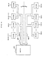
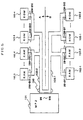
- Figs. 9 and 10 illustrate methods of packaging the wiring substrate 10 embodying the present invention as shown in Fig. 8.
- MPU 101, FPU 104, ROMs 103-1, 103-2 and RAM 102-1, 102-2 are mounted on the surface (B side) shown in Fig. 9.
- the storage element, ROMs 103-1, 103-2 and RAMs 102-1, 102-2 connected to the data lines which belong to the bus 100-1 are mounted on this surface as shown in Fig. 5.
- DMAC 105 the gate array 110, ROMs 103-3, 103-4 and RAMs 102-3, 102-4 are mounted on the surface (A side) shown in Fig. 10.
- the wiring substrate 10 can be made smaller. Moreover, the concentration of heat and wiring to one side is made avoidable by splitting LSI, MPU 101, FPU 104, DMAC 105 and the gate array 110 into two groups, each having a large chip size and many input-output signal lines, and allotting them to the respective sides. In view of thermal resistance, chemical stability and the like, a ceramic substrate is fit for use as the wiring substrate 10 when it is employed in space where reliability is required.
- Fig. 11 illustrates a package embodying the present invention.
- Ceramic caps 50 are attached to the respective sides of the ceramic wiring substrate 10 to hermetically seal bare chips such as MPU 101 mounted thereon.
- the inside thus hermetically sealed by the caps 50 is kept under vacuum or filled with an inactive gas of nitrogen, helium or the like. If helium is filled up, it will conveniently be used for leakage checking when the airtightness of the seal is checked.
- the package tends to become large and the volume of the air inside the caps 50 also tends to increase.
- the molten solder may be drawn into or jutted out of the caps 50 due to the difference in pressure between the inside and the outside as the solder cools.
- One of the measures to be taken to prevent the molten solder from being drawn into or jutted out of the caps 50 even though a package is large is to bore ventilating holes 51 into them and to cover the holes 51 with lids 52 or the like after the contents are hermetically sealed with the inactive gas encapsulated.
- a plurality of semiconductor elements can be accommodated in a single package and the number of signal lines to be led out of the package is reducible, so that the package size is decreased. Therefore, a small lightweight electronic apparatus is made available.
- the invention is related to an electronic circuit which comprises at least two semiconductor chips which are all connected to a bus line and which are connected to one wiring substrate.
- the bus line includes two data bus lines.
- the semiconductor chips connected with one data bus line are formed on one side of the wiring substrate and semiconductor chips connected with the other data bus line are formed on the other side of the wiring substrate.
- the semiconductor chips connected with said data bus lines are random access memories and read only memories.
- the wiring substrate is a multilayer wiring substrate.
- the electronic circuit package further comprises an insulating layer partially formed on the surface of the multilayer wiring substrate and a die bonding ground formed on the surface of the insulating layer, in order to use a portion of the multilayer wiring substrate under the die bonding ground as a wiring or a via hole region, wherein at least one of the semiconductor chips is formed on the die bonding ground.
- the invention involves an electronic circuit package which comprises a multilayer wiring substrate on which at least one semiconductor chip is provided, an insulating layer partially formed on the surface of the multilayer wiring substrate, and a die bonding ground formed on the surface of the insulating layer in order to use a portion of the multilayer wiring substrate under the die bonding ground as a wiring or a via hole region, wherein at least one of the semiconductor chips is formed on the die bonding ground.
- the electronic circuit package further comprises wiring conductors from a wiring pad and via holes formed in the periphery and inside of the die bonding ground, wherein the wiring conductors are connected to a wiring conductor of a different wiring layer in the multilayer wiring substrate through the via holes.
- the via hole formed in the periphery of the die bonding ground and the via hole formed inside of the die bonding ground are arranged alternately.
- the semiconductor chips include a microprocessing unit and a checking unit for detecting errors and faults of the microprocessing unit.
- the semiconductor chips include a random access memory and an error correction code unit for detecting errors of said random access memory and for correcting said errors.
- the checking unit or the error correction code unit is included in a gate array.
- the semiconductor chips include a gate array.
- the bus line includes means for connecting to a memory outside of the wiring substrate, wherein the memory stores programs for processing of said electronic apparatus.
- the present invention relates also to an electronic system comprising an electronic circuit package as defined above.
Landscapes
- Semiconductor Integrated Circuits (AREA)
- Techniques For Improving Reliability Of Storages (AREA)
- Test And Diagnosis Of Digital Computers (AREA)
- Microcomputers (AREA)
- Detection And Correction Of Errors (AREA)
- Semiconductor Memories (AREA)
- Structures For Mounting Electric Components On Printed Circuit Boards (AREA)
- Structure Of Printed Boards (AREA)
- Design And Manufacture Of Integrated Circuits (AREA)
Priority Applications (1)
| Application Number | Priority Date | Filing Date | Title |
|---|---|---|---|
| EP03025414A EP1394557A3 (de) | 1991-02-28 | 1992-02-27 | Elektronischer Apparat |
Applications Claiming Priority (4)
| Application Number | Priority Date | Filing Date | Title |
|---|---|---|---|
| JP34038/91 | 1991-02-28 | ||
| JP3403891 | 1991-02-28 | ||
| JP3034038A JP2960560B2 (ja) | 1991-02-28 | 1991-02-28 | 超小型電子機器 |
| EP92103361A EP0501474B1 (de) | 1991-02-28 | 1992-02-27 | Packung für elektronische Schaltung |
Related Parent Applications (2)
| Application Number | Title | Priority Date | Filing Date |
|---|---|---|---|
| EP92103361.9 Division | 1992-02-27 | ||
| EP92103361A Division EP0501474B1 (de) | 1991-02-28 | 1992-02-27 | Packung für elektronische Schaltung |
Related Child Applications (1)
| Application Number | Title | Priority Date | Filing Date |
|---|---|---|---|
| EP03025414A Division EP1394557A3 (de) | 1991-02-28 | 1992-02-27 | Elektronischer Apparat |
Publications (2)
| Publication Number | Publication Date |
|---|---|
| EP0786809A1 true EP0786809A1 (de) | 1997-07-30 |
| EP0786809B1 EP0786809B1 (de) | 2004-01-28 |
Family
ID=12403153
Family Applications (3)
| Application Number | Title | Priority Date | Filing Date |
|---|---|---|---|
| EP97100415A Expired - Lifetime EP0786809B1 (de) | 1991-02-28 | 1992-02-27 | Packung für elektronische Schaltung |
| EP92103361A Expired - Lifetime EP0501474B1 (de) | 1991-02-28 | 1992-02-27 | Packung für elektronische Schaltung |
| EP03025414A Withdrawn EP1394557A3 (de) | 1991-02-28 | 1992-02-27 | Elektronischer Apparat |
Family Applications After (2)
| Application Number | Title | Priority Date | Filing Date |
|---|---|---|---|
| EP92103361A Expired - Lifetime EP0501474B1 (de) | 1991-02-28 | 1992-02-27 | Packung für elektronische Schaltung |
| EP03025414A Withdrawn EP1394557A3 (de) | 1991-02-28 | 1992-02-27 | Elektronischer Apparat |
Country Status (5)
| Country | Link |
|---|---|
| US (11) | US5468992A (de) |
| EP (3) | EP0786809B1 (de) |
| JP (1) | JP2960560B2 (de) |
| CA (1) | CA2061949C (de) |
| DE (2) | DE69233063T2 (de) |
Families Citing this family (42)
| Publication number | Priority date | Publication date | Assignee | Title |
|---|---|---|---|---|
| JP2960560B2 (ja) * | 1991-02-28 | 1999-10-06 | 株式会社日立製作所 | 超小型電子機器 |
| US5721452A (en) * | 1995-08-16 | 1998-02-24 | Micron Technology, Inc. | Angularly offset stacked die multichip device and method of manufacture |
| US5982185A (en) * | 1996-07-01 | 1999-11-09 | Micron Technology, Inc. | Direct connect carrier for testing semiconductor dice and method of fabrication |
| US6639416B1 (en) | 1996-07-02 | 2003-10-28 | Micron Technology, Inc. | Method and apparatus for testing semiconductor dice |
| US5929647A (en) * | 1996-07-02 | 1999-07-27 | Micron Technology, Inc. | Method and apparatus for testing semiconductor dice |
| US6255833B1 (en) | 1997-03-04 | 2001-07-03 | Micron Technology, Inc. | Method for testing semiconductor dice and chip scale packages |
| SE509570C2 (sv) * | 1996-10-21 | 1999-02-08 | Ericsson Telefon Ab L M | Temperaturkompenserande organ och förfarande vid montering av elektronik på ett mönsterkort |
| JP3942198B2 (ja) * | 1996-12-04 | 2007-07-11 | 株式会社ルネサステクノロジ | 半導体集積回路装置 |
| DE19724053A1 (de) * | 1997-06-07 | 1998-12-10 | Biotronik Mess & Therapieg | Elektronische Speichervorrichtung, insbesondere zur Anwendung bei implantierbaren medizinischen Geräten |
| JP3896250B2 (ja) * | 1997-11-06 | 2007-03-22 | 株式会社ルネサステクノロジ | 情報処理装置 |
| US5933327A (en) * | 1998-04-03 | 1999-08-03 | Ericsson, Inc. | Wire bond attachment of a integrated circuit package to a heat sink |
| JP2000077609A (ja) * | 1998-08-28 | 2000-03-14 | Hitachi Ltd | 半導体集積回路装置 |
| US6281042B1 (en) | 1998-08-31 | 2001-08-28 | Micron Technology, Inc. | Structure and method for a high performance electronic packaging assembly |
| US6586835B1 (en) * | 1998-08-31 | 2003-07-01 | Micron Technology, Inc. | Compact system module with built-in thermoelectric cooling |
| US6392296B1 (en) | 1998-08-31 | 2002-05-21 | Micron Technology, Inc. | Silicon interposer with optical connections |
| US6154364A (en) * | 1998-11-19 | 2000-11-28 | Delco Electronics Corp. | Circuit board assembly with IC device mounted thereto |
| US6255852B1 (en) | 1999-02-09 | 2001-07-03 | Micron Technology, Inc. | Current mode signal interconnects and CMOS amplifier |
| US7554829B2 (en) * | 1999-07-30 | 2009-06-30 | Micron Technology, Inc. | Transmission lines for CMOS integrated circuits |
| US6406940B1 (en) | 2000-08-14 | 2002-06-18 | Intermedics Inc. | Method and apparatus for stacking IC devices |
| US6349050B1 (en) * | 2000-10-10 | 2002-02-19 | Rambus, Inc. | Methods and systems for reducing heat flux in memory systems |
| US7101770B2 (en) | 2002-01-30 | 2006-09-05 | Micron Technology, Inc. | Capacitive techniques to reduce noise in high speed interconnections |
| US7235457B2 (en) | 2002-03-13 | 2007-06-26 | Micron Technology, Inc. | High permeability layered films to reduce noise in high speed interconnects |
| US7606293B2 (en) * | 2002-10-25 | 2009-10-20 | Gct Semiconductor, Inc. | Bidirectional turbo ISI canceller-based DSSS receiver for high-speed wireless LAN |
| US7230146B2 (en) | 2003-10-27 | 2007-06-12 | Honeywell International Inc. | Process for producing fluoropropenes |
| US7444546B2 (en) * | 2003-04-17 | 2008-10-28 | Arm Limited | On-board diagnostic circuit for an integrated circuit |
| US7302025B2 (en) * | 2003-09-25 | 2007-11-27 | Analog Devices, Inc. | Efficient joint equalization/decoding method and apparatus for Complementary-Code-Keying based systems |
| US8324725B2 (en) * | 2004-09-27 | 2012-12-04 | Formfactor, Inc. | Stacked die module |
| US7015823B1 (en) | 2004-10-15 | 2006-03-21 | Systran Federal Corporation | Tamper resistant circuit boards |
| US7281667B2 (en) * | 2005-04-14 | 2007-10-16 | International Business Machines Corporation | Method and structure for implementing secure multichip modules for encryption applications |
| US7582951B2 (en) * | 2005-10-20 | 2009-09-01 | Broadcom Corporation | Methods and apparatus for improved thermal performance and electromagnetic interference (EMI) shielding in leadframe integrated circuit (IC) packages |
| US7808087B2 (en) * | 2006-06-01 | 2010-10-05 | Broadcom Corporation | Leadframe IC packages having top and bottom integrated heat spreaders |
| JP4863953B2 (ja) * | 2007-08-30 | 2012-01-25 | 日立オートモティブシステムズ株式会社 | 物理量変換センサ及びそれを用いたモータ制御システム |
| US8443175B2 (en) * | 2009-07-10 | 2013-05-14 | Via Technologies, Inc. | Microprocessor with first processor for debugging second processor |
| US8495344B2 (en) * | 2010-01-22 | 2013-07-23 | Via Technologies, Inc. | Simultaneous execution resumption of multiple processor cores after core state information dump to facilitate debugging via multi-core processor simulator using the state information |
| US8762779B2 (en) * | 2010-01-22 | 2014-06-24 | Via Technologies, Inc. | Multi-core processor with external instruction execution rate heartbeat |
| US8639919B2 (en) | 2011-01-18 | 2014-01-28 | Via Technologies, Inc. | Tracer configuration and enablement by reset microcode |
| US9153508B2 (en) | 2011-08-17 | 2015-10-06 | Rambus Inc. | Multi-chip package and interposer with signal line compression |
| US8634221B2 (en) | 2011-11-01 | 2014-01-21 | Avago Technologies General Ip (Singapore) Pte. Ltd. | Memory system that utilizes a wide input/output (I/O) interface to interface memory storage with an interposer and that utilizes a SerDes interface to interface a memory controller with an integrated circuit, and a method |
| KR102104578B1 (ko) * | 2013-08-30 | 2020-04-27 | 에스케이하이닉스 주식회사 | 데이터 비트 인버전 기능을 갖는 반도체 장치 |
| EP3478936B1 (de) | 2016-09-27 | 2022-11-09 | Halliburton Energy Services, Inc. | Formationstester mit reaktivem filtermaterial |
| CN112927747B (zh) * | 2021-04-22 | 2021-09-21 | 中科一芯科技(深圳)有限公司 | 一种嵌入式存储芯片打线导致芯片失效的解决方法 |
| CN114679424B (zh) * | 2022-03-31 | 2023-07-07 | 中科芯集成电路有限公司 | 一种多裸芯集成微系统dma实现方法 |
Citations (5)
| Publication number | Priority date | Publication date | Assignee | Title |
|---|---|---|---|---|
| US4763188A (en) * | 1986-08-08 | 1988-08-09 | Thomas Johnson | Packaging system for multiple semiconductor devices |
| EP0294015A1 (de) * | 1987-03-13 | 1988-12-07 | Citizen Watch Co. Ltd. | Anordnung mit Platte zur Bestückung mehrerer Halbleiterchips |
| EP0339154A2 (de) * | 1988-04-26 | 1989-11-02 | Citizen Watch Co. Ltd. | Speicherkarte |
| EP0346629A2 (de) * | 1988-06-15 | 1989-12-20 | International Business Machines Corporation | Architektur und Schnittstelle für Speicherkarten |
| EP0454447A2 (de) * | 1990-04-26 | 1991-10-30 | Hitachi, Ltd. | Zusammenbau von Halbleiteranordnungen |
Family Cites Families (93)
| Publication number | Priority date | Publication date | Assignee | Title |
|---|---|---|---|---|
| US33013A (en) * | 1861-08-06 | Improvement in seed-sowing machines | ||
| US24389A (en) * | 1859-06-14 | Improvement in horse-rakes | ||
| US56911A (en) * | 1866-08-07 | Improved washing-machine | ||
| US22739A (en) * | 1859-01-25 | Antonio metjcci | ||
| US40261A (en) * | 1863-10-13 | Improvement in granaries | ||
| US131228A (en) * | 1872-09-10 | Improvement in stump-extractors | ||
| US3851221A (en) * | 1972-11-30 | 1974-11-26 | P Beaulieu | Integrated circuit package |
| US4172282A (en) * | 1976-10-29 | 1979-10-23 | International Business Machines Corporation | Processor controlled memory refresh |
| US4144561A (en) * | 1977-07-08 | 1979-03-13 | Xerox Corporation | Chip topography for MOS integrated circuitry microprocessor chip |
| JPS5537641A (en) | 1978-09-08 | 1980-03-15 | Fujitsu Ltd | Synchronization system for doubled processor |
| US4245273A (en) | 1979-06-29 | 1981-01-13 | International Business Machines Corporation | Package for mounting and interconnecting a plurality of large scale integrated semiconductor devices |
| IT1128896B (it) * | 1980-07-03 | 1986-06-04 | Olivetti & Co Spa | Apparecchiatura di elaborazione dati con memoria permanente programmabile |
| US4443278A (en) * | 1981-05-26 | 1984-04-17 | International Business Machines Corporation | Inspection of multilayer ceramic circuit modules by electrical inspection of green specimens |
| US4504784A (en) * | 1981-07-02 | 1985-03-12 | International Business Machines Corporation | Method of electrically testing a packaging structure having N interconnected integrated circuit chips |
| US4441075A (en) * | 1981-07-02 | 1984-04-03 | International Business Machines Corporation | Circuit arrangement which permits the testing of each individual chip and interchip connection in a high density packaging structure having a plurality of interconnected chips, without any physical disconnection |
| US4602271A (en) * | 1981-07-22 | 1986-07-22 | International Business Machines Corporation | Personalizable masterslice substrate for semiconductor chips |
| US4432055A (en) * | 1981-09-29 | 1984-02-14 | Honeywell Information Systems Inc. | Sequential word aligned addressing apparatus |
| JPS5961152A (ja) * | 1982-09-30 | 1984-04-07 | Fujitsu Ltd | 半導体装置 |
| US5149940A (en) * | 1983-02-24 | 1992-09-22 | Beckworth Davis International Inc. | Method for controlling and synchronizing a welding power supply |
| JPS6050940A (ja) * | 1983-08-31 | 1985-03-22 | Toshiba Corp | 半導体集積回路 |
| US4649474A (en) * | 1983-09-23 | 1987-03-10 | Western Digital Corporation | Chip topography for a MOS disk memory controller circuit |
| US4618953A (en) * | 1984-05-01 | 1986-10-21 | Pitney Bowes Inc. | Watchdog circuit |
| US4577293A (en) * | 1984-06-01 | 1986-03-18 | International Business Machines Corporation | Distributed, on-chip cache |
| JPS617656A (ja) * | 1984-06-22 | 1986-01-14 | Toshiba Corp | マルチチップパッケ−ジ |
| JPS61112345A (ja) * | 1984-11-07 | 1986-05-30 | Toshiba Corp | 半導体装置の製造方法 |
| US4803682A (en) * | 1985-03-04 | 1989-02-07 | Sanyo Electric Co., Ltd. | Resetting system |
| US4692839A (en) * | 1985-06-24 | 1987-09-08 | Digital Equipment Corporation | Multiple chip interconnection system and package |
| GB2182176B (en) * | 1985-09-25 | 1989-09-20 | Ncr Co | Data security device for protecting stored data |
| JPS6281745A (ja) * | 1985-10-05 | 1987-04-15 | Fujitsu Ltd | ウエハ−規模のlsi半導体装置とその製造方法 |
| US4922363A (en) * | 1985-10-17 | 1990-05-01 | General Electric Company | Contactor control system |
| US4746966A (en) * | 1985-10-21 | 1988-05-24 | International Business Machines Corporation | Logic-circuit layout for large-scale integrated circuits |
| JPS62162749A (ja) | 1986-01-13 | 1987-07-18 | Komatsu Ltd | 内燃機関発電機 |
| US4752927A (en) * | 1986-04-09 | 1988-06-21 | Tektronix, Inc. | Synchronous changeover |
| GB2195478B (en) * | 1986-09-24 | 1990-06-13 | Ncr Co | Security device for sensitive data |
| US4918811A (en) * | 1986-09-26 | 1990-04-24 | General Electric Company | Multichip integrated circuit packaging method |
| US4783695A (en) * | 1986-09-26 | 1988-11-08 | General Electric Company | Multichip integrated circuit packaging configuration and method |
| US4773044A (en) * | 1986-11-21 | 1988-09-20 | Advanced Micro Devices, Inc | Array-word-organized display memory and address generator with time-multiplexed address bus |
| JPS63245952A (ja) * | 1987-04-01 | 1988-10-13 | Hitachi Ltd | マルチチップモジュ−ル構造体 |
| US4993148A (en) * | 1987-05-19 | 1991-02-19 | Mitsubishi Denki Kabushiki Kaisha | Method of manufacturing a circuit board |
| US5243208A (en) * | 1987-05-27 | 1993-09-07 | Hitachi, Ltd. | Semiconductor integrated circuit device having a gate array with a ram and by-pass signal lines which interconnect a logic section and I/O unit circuit of the gate array |
| US5138438A (en) * | 1987-06-24 | 1992-08-11 | Akita Electronics Co. Ltd. | Lead connections means for stacked tab packaged IC chips |
| US4947183A (en) * | 1987-11-14 | 1990-08-07 | Ricoh Company, Ltd. | Edge type thermal printhead |
| US5028986A (en) * | 1987-12-28 | 1991-07-02 | Hitachi, Ltd. | Semiconductor device and semiconductor module with a plurality of stacked semiconductor devices |
| JPH07107956B2 (ja) | 1988-02-29 | 1995-11-15 | 沖電気工業株式会社 | プロセッサ塔載回路 |
| JP2645068B2 (ja) | 1988-04-08 | 1997-08-25 | 株式会社東芝 | メモリモジュール |
| US5072283A (en) * | 1988-04-12 | 1991-12-10 | Bolger Justin C | Pre-formed chip carrier cavity package |
| US5185717A (en) * | 1988-08-05 | 1993-02-09 | Ryoichi Mori | Tamper resistant module having logical elements arranged in multiple layers on the outer surface of a substrate to protect stored information |
| JP2592308B2 (ja) * | 1988-09-30 | 1997-03-19 | 株式会社日立製作所 | 半導体パッケージ及びそれを用いたコンピュータ |
| CA2002213C (en) * | 1988-11-10 | 1999-03-30 | Iwona Turlik | High performance integrated circuit chip package and method of making same |
| US4933898A (en) * | 1989-01-12 | 1990-06-12 | General Instrument Corporation | Secure integrated circuit chip with conductive shield |
| US4979289A (en) * | 1989-02-10 | 1990-12-25 | Honeywell Inc. | Method of die bonding semiconductor chip by using removable non-wettable by solder frame |
| JPH02219254A (ja) * | 1989-02-20 | 1990-08-31 | Hitachi Ltd | 半導体集積回路装置 |
| US4993143A (en) * | 1989-03-06 | 1991-02-19 | Delco Electronics Corporation | Method of making a semiconductive structure useful as a pressure sensor |
| JPH02289014A (ja) | 1989-03-17 | 1990-11-29 | Nec Corp | Dram制御装置 |
| US5285107A (en) * | 1989-04-20 | 1994-02-08 | Sanyo Electric Co., Ltd. | Hybrid integrated circuit device |
| DE68916784T2 (de) * | 1989-04-20 | 1995-01-05 | Ibm | Integrierte Schaltungspackung. |
| US5068850A (en) * | 1989-06-12 | 1991-11-26 | Moore Industries-International, Inc. | Parameter value communication system |
| US4922379A (en) * | 1989-07-18 | 1990-05-01 | Hughes Aircraft Company | Power semiconductor package |
| GB8918482D0 (en) * | 1989-08-14 | 1989-09-20 | Inmos Ltd | Packaging semiconductor chips |
| US5182632A (en) * | 1989-11-22 | 1993-01-26 | Tactical Fabs, Inc. | High density multichip package with interconnect structure and heatsink |
| US5019943A (en) * | 1990-02-14 | 1991-05-28 | Unisys Corporation | High density chip stack having a zigzag-shaped face which accommodates connections between chips |
| US5128737A (en) * | 1990-03-02 | 1992-07-07 | Silicon Dynamics, Inc. | Semiconductor integrated circuit fabrication yield improvements |
| US5200810A (en) * | 1990-04-05 | 1993-04-06 | General Electric Company | High density interconnect structure with top mounted components |
| US5081563A (en) * | 1990-04-27 | 1992-01-14 | International Business Machines Corporation | Multi-layer package incorporating a recessed cavity for a semiconductor chip |
| US5050039A (en) * | 1990-06-26 | 1991-09-17 | Digital Equipment Corporation | Multiple circuit chip mounting and cooling arrangement |
| US5241456A (en) * | 1990-07-02 | 1993-08-31 | General Electric Company | Compact high density interconnect structure |
| US5768613A (en) * | 1990-07-06 | 1998-06-16 | Advanced Micro Devices, Inc. | Computing apparatus configured for partitioned processing |
| DE69133311T2 (de) * | 1990-10-15 | 2004-06-24 | Aptix Corp., San Jose | Verbindungssubstrat mit integrierter Schaltung zur programmierbaren Verbindung und Probenuntersuchung |
| JP2960560B2 (ja) * | 1991-02-28 | 1999-10-06 | 株式会社日立製作所 | 超小型電子機器 |
| JPH0833978B2 (ja) * | 1991-04-26 | 1996-03-29 | インターナショナル・ビジネス・マシーンズ・コーポレイション | 磁気ヘッド及びその製造方法 |
| US5237203A (en) * | 1991-05-03 | 1993-08-17 | Trw Inc. | Multilayer overlay interconnect for high-density packaging of circuit elements |
| US5121293A (en) * | 1991-08-08 | 1992-06-09 | Sun Microsystems, Inc. | Method and apparatus for interconnecting devices using tab in board technology |
| JP2634516B2 (ja) * | 1991-10-15 | 1997-07-30 | 三菱電機株式会社 | 反転型icの製造方法、反転型ic、icモジュール |
| US5576554A (en) * | 1991-11-05 | 1996-11-19 | Monolithic System Technology, Inc. | Wafer-scale integrated circuit interconnect structure architecture |
| US5801432A (en) * | 1992-06-04 | 1998-09-01 | Lsi Logic Corporation | Electronic system using multi-layer tab tape semiconductor device having distinct signal, power and ground planes |
| JP3210466B2 (ja) * | 1993-02-25 | 2001-09-17 | 株式会社リコー | Cpuコア、該cpuコアを有するasic、及び該asicを備えたエミュレーションシステム |
| US5391917A (en) * | 1993-05-10 | 1995-02-21 | International Business Machines Corporation | Multiprocessor module packaging |
| KR0147259B1 (ko) * | 1994-10-27 | 1998-08-01 | 김광호 | 적층형 패키지 및 그 제조방법 |
| JPH08147197A (ja) * | 1994-11-25 | 1996-06-07 | Sanyo Electric Co Ltd | 障害情報を記憶する情報処理装置 |
| JP2677216B2 (ja) | 1994-12-16 | 1997-11-17 | 株式会社押野電気製作所 | パネル・プリント基板用小形ランプソケット装置 |
| US5552633A (en) * | 1995-06-06 | 1996-09-03 | Martin Marietta Corporation | Three-dimensional multimodule HDI arrays with heat spreading |
| JPH11120075A (ja) * | 1997-10-20 | 1999-04-30 | Toshiba Corp | 半導体記憶装置及び半導体記憶システム |
| US6198118B1 (en) * | 1998-03-09 | 2001-03-06 | Integration Associates, Inc. | Distributed photodiode structure |
| US6268660B1 (en) * | 1999-03-05 | 2001-07-31 | International Business Machines Corporation | Silicon packaging with through wafer interconnects |
| JP2000315776A (ja) * | 1999-05-06 | 2000-11-14 | Hitachi Ltd | 半導体装置 |
| JP2001024150A (ja) * | 1999-07-06 | 2001-01-26 | Sony Corp | 半導体装置 |
| US6612605B2 (en) * | 1999-09-29 | 2003-09-02 | K-2 Corporation | Integrated modular glide board |
| JP4569912B2 (ja) * | 2000-03-10 | 2010-10-27 | エルピーダメモリ株式会社 | メモリシステム |
| JP4569913B2 (ja) * | 2000-03-10 | 2010-10-27 | エルピーダメモリ株式会社 | メモリモジュール |
| KR100336281B1 (ko) * | 2000-04-20 | 2002-05-13 | 윤종용 | 수리할 수 있는 멀티 칩 패키지 |
| JP2002108835A (ja) * | 2000-09-29 | 2002-04-12 | Mitsubishi Electric Corp | 車載電子制御装置 |
| PL209035B1 (pl) * | 2001-11-16 | 2011-07-29 | Ami Agrolinz Melamine Int Gmbh | Sposób wytwarzania melaminy pozbawionej melemu oraz bezprzeponowa chłodnica do stosowania tego sposobu |
| US7246245B2 (en) * | 2002-01-10 | 2007-07-17 | Broadcom Corporation | System on a chip for network storage devices |
-
1991
- 1991-02-28 JP JP3034038A patent/JP2960560B2/ja not_active Expired - Lifetime
-
1992
- 1992-02-27 EP EP97100415A patent/EP0786809B1/de not_active Expired - Lifetime
- 1992-02-27 DE DE69233063T patent/DE69233063T2/de not_active Expired - Lifetime
- 1992-02-27 EP EP92103361A patent/EP0501474B1/de not_active Expired - Lifetime
- 1992-02-27 DE DE1992633297 patent/DE69233297T2/de not_active Expired - Lifetime
- 1992-02-27 EP EP03025414A patent/EP1394557A3/de not_active Withdrawn
- 1992-02-27 CA CA002061949A patent/CA2061949C/en not_active Expired - Lifetime
- 1992-02-28 US US07/843,234 patent/US5468992A/en not_active Expired - Lifetime
-
1995
- 1995-09-05 US US08/523,346 patent/US5614761A/en not_active Expired - Lifetime
-
1996
- 1996-11-18 US US08/746,942 patent/US5789805A/en not_active Expired - Lifetime
-
1998
- 1998-06-10 US US09/095,049 patent/US6195742B1/en not_active Expired - Fee Related
-
1999
- 1999-03-18 US US09/271,448 patent/US6223273B1/en not_active Expired - Fee Related
-
2001
- 2001-02-28 US US09/793,968 patent/US6584004B2/en not_active Expired - Fee Related
-
2003
- 2003-02-24 US US10/370,518 patent/US6728904B2/en not_active Expired - Fee Related
-
2004
- 2004-02-26 US US10/786,008 patent/US7120069B2/en not_active Expired - Fee Related
-
2005
- 2005-07-14 US US11/180,733 patent/US7233534B2/en not_active Expired - Fee Related
-
2007
- 2007-03-07 US US11/714,747 patent/US7425763B2/en not_active Expired - Fee Related
-
2008
- 2008-08-07 US US12/222,329 patent/US7701743B2/en not_active Expired - Fee Related
Patent Citations (5)
| Publication number | Priority date | Publication date | Assignee | Title |
|---|---|---|---|---|
| US4763188A (en) * | 1986-08-08 | 1988-08-09 | Thomas Johnson | Packaging system for multiple semiconductor devices |
| EP0294015A1 (de) * | 1987-03-13 | 1988-12-07 | Citizen Watch Co. Ltd. | Anordnung mit Platte zur Bestückung mehrerer Halbleiterchips |
| EP0339154A2 (de) * | 1988-04-26 | 1989-11-02 | Citizen Watch Co. Ltd. | Speicherkarte |
| EP0346629A2 (de) * | 1988-06-15 | 1989-12-20 | International Business Machines Corporation | Architektur und Schnittstelle für Speicherkarten |
| EP0454447A2 (de) * | 1990-04-26 | 1991-10-30 | Hitachi, Ltd. | Zusammenbau von Halbleiteranordnungen |
Non-Patent Citations (6)
| Title |
|---|
| "Collection of Papers at 32nd Space Science and Technology Federation Lecture Meeting.", article GOKE ET AL.: "Development of LSI for Radiatio Resistant 16-Bit Microprocessor.", pages: 10 - 411 |
| "DOUBLE-DENSITY MEMORY CARRIER", IBM TECHNICAL DISCLOSURE BULLETIN, vol. 32, no. 5B, October 1989 (1989-10-01), pages 77, XP000049167 * |
| "High Density Multilayer Ceramic Module", IBM TECHNICAL DISCLOSURE BULLETIN, vol. 20, no. 11b, April 1978 (1978-04-01), NEW YORK US, pages 4771 - 4773, XP002030096 * |
| "Microsystem Package for Chips", IBM TECHNICAL DISCLOSURE BULLETIN, vol. 24, no. 3, August 1981 (1981-08-01), NEW YORK US, pages 1657 - 1658, XP002030097 * |
| "Nikkei Micro Device.", 1989, pages: 32 - 40 |
| "Research Material, 24th FTC Study Meeting.", article TSUCHIMURA ET AL.: "Trial Manufacture and Evaluation of Fault Tolerant Quartz Oscillation IC." |
Also Published As
| Publication number | Publication date |
|---|---|
| US7120069B2 (en) | 2006-10-10 |
| DE69233063D1 (de) | 2003-06-26 |
| JP2960560B2 (ja) | 1999-10-06 |
| EP0501474A2 (de) | 1992-09-02 |
| EP0501474A3 (en) | 1993-01-13 |
| US6195742B1 (en) | 2001-02-27 |
| US5614761A (en) | 1997-03-25 |
| CA2061949C (en) | 1998-01-27 |
| DE69233297T2 (de) | 2004-11-18 |
| JPH04273470A (ja) | 1992-09-29 |
| EP1394557A3 (de) | 2004-10-20 |
| US6223273B1 (en) | 2001-04-24 |
| US20050248017A1 (en) | 2005-11-10 |
| US20070158814A1 (en) | 2007-07-12 |
| CA2061949A1 (en) | 1992-08-29 |
| US6728904B2 (en) | 2004-04-27 |
| US7425763B2 (en) | 2008-09-16 |
| EP1394557A2 (de) | 2004-03-03 |
| US20010010064A1 (en) | 2001-07-26 |
| US5789805A (en) | 1998-08-04 |
| DE69233063T2 (de) | 2004-09-16 |
| US20030156441A1 (en) | 2003-08-21 |
| US20080303175A1 (en) | 2008-12-11 |
| EP0501474B1 (de) | 2003-05-21 |
| US20040164324A1 (en) | 2004-08-26 |
| US7233534B2 (en) | 2007-06-19 |
| US5468992A (en) | 1995-11-21 |
| US6584004B2 (en) | 2003-06-24 |
| EP0786809B1 (de) | 2004-01-28 |
| US7701743B2 (en) | 2010-04-20 |
| DE69233297D1 (de) | 2004-03-04 |
Similar Documents
| Publication | Publication Date | Title |
|---|---|---|
| US5468992A (en) | Electronic circuit package including plural bare chips mounted on a single wiring substrate | |
| US6555399B1 (en) | Double-packaged multichip semiconductor module | |
| US6774475B2 (en) | Vertically stacked memory chips in FBGA packages | |
| US6720652B2 (en) | Apparatus providing redundancy for fabricating highly reliable memory modules | |
| EP0713609B1 (de) | Ic-stapel als ersatz für einzelnen ic | |
| US20020027813A1 (en) | Redundancy mapping in a multichip semiconductor package | |
| US6121681A (en) | Semiconductor device | |
| US7057964B2 (en) | Semiconductor memory device with efficient multiplexing of I/O pad in multi-chip package | |
| CN108701686A (zh) | 具有复制裸片接合垫的半导体装置及相关联装置封装及其制造方法 | |
| JP2943781B2 (ja) | 半導体メモリ | |
| CA2205528C (en) | Data processing apparatus and method of data transmission of data processing apparatus | |
| US6222211B1 (en) | Memory package method and apparatus | |
| JP3345381B2 (ja) | 情報処理装置 | |
| JP3283815B2 (ja) | 半導体集積回路モジュール | |
| JPS60200537A (ja) | テスト専用端子付半導体装置 | |
| JPH11242898A (ja) | メモリモジュールと電子装置 | |
| WO1998038680A1 (en) | Memory module |
Legal Events
| Date | Code | Title | Description |
|---|---|---|---|
| PUAI | Public reference made under article 153(3) epc to a published international application that has entered the european phase |
Free format text: ORIGINAL CODE: 0009012 |
|
| 17P | Request for examination filed |
Effective date: 19970113 |
|
| AC | Divisional application: reference to earlier application |
Ref document number: 501474 Country of ref document: EP |
|
| AK | Designated contracting states |
Kind code of ref document: A1 Designated state(s): DE FR GB IT NL |
|
| 17Q | First examination report despatched |
Effective date: 19980909 |
|
| GRAP | Despatch of communication of intention to grant a patent |
Free format text: ORIGINAL CODE: EPIDOSNIGR1 |
|
| GRAS | Grant fee paid |
Free format text: ORIGINAL CODE: EPIDOSNIGR3 |
|
| GRAA | (expected) grant |
Free format text: ORIGINAL CODE: 0009210 |
|
| AC | Divisional application: reference to earlier application |
Ref document number: 0501474 Country of ref document: EP Kind code of ref document: P |
|
| AK | Designated contracting states |
Kind code of ref document: B1 Designated state(s): DE FR GB IT NL |
|
| REG | Reference to a national code |
Ref country code: GB Ref legal event code: FG4D |
|
| REF | Corresponds to: |
Ref document number: 69233297 Country of ref document: DE Date of ref document: 20040304 Kind code of ref document: P |
|
| ET | Fr: translation filed | ||
| PLBE | No opposition filed within time limit |
Free format text: ORIGINAL CODE: 0009261 |
|
| STAA | Information on the status of an ep patent application or granted ep patent |
Free format text: STATUS: NO OPPOSITION FILED WITHIN TIME LIMIT |
|
| 26N | No opposition filed |
Effective date: 20041029 |
|
| REG | Reference to a national code |
Ref country code: GB Ref legal event code: 732E Free format text: REGISTERED BETWEEN 20100204 AND 20100211 |
|
| REG | Reference to a national code |
Ref country code: FR Ref legal event code: TP |
|
| NLS | Nl: assignments of ep-patents |
Owner name: RISING SILICON, INCORPORATED Effective date: 20100122 |
|
| PGFP | Annual fee paid to national office [announced via postgrant information from national office to epo] |
Ref country code: FR Payment date: 20110218 Year of fee payment: 20 Ref country code: NL Payment date: 20110216 Year of fee payment: 20 Ref country code: IT Payment date: 20110219 Year of fee payment: 20 Ref country code: DE Payment date: 20110223 Year of fee payment: 20 |
|
| PGFP | Annual fee paid to national office [announced via postgrant information from national office to epo] |
Ref country code: GB Payment date: 20110223 Year of fee payment: 20 |
|
| REG | Reference to a national code |
Ref country code: DE Ref legal event code: R071 Ref document number: 69233297 Country of ref document: DE |
|
| REG | Reference to a national code |
Ref country code: DE Ref legal event code: R071 Ref document number: 69233297 Country of ref document: DE |
|
| REG | Reference to a national code |
Ref country code: NL Ref legal event code: V4 Effective date: 20120227 |
|
| REG | Reference to a national code |
Ref country code: GB Ref legal event code: PE20 Expiry date: 20120226 |
|
| PG25 | Lapsed in a contracting state [announced via postgrant information from national office to epo] |
Ref country code: DE Free format text: LAPSE BECAUSE OF EXPIRATION OF PROTECTION Effective date: 20120228 |
|
| PG25 | Lapsed in a contracting state [announced via postgrant information from national office to epo] |
Ref country code: GB Free format text: LAPSE BECAUSE OF EXPIRATION OF PROTECTION Effective date: 20120226 |