EP0788657B1 - Zellendesign für hochauflösendes aktiv-matrix-lcd - Google Patents
Zellendesign für hochauflösendes aktiv-matrix-lcd Download PDFInfo
- Publication number
- EP0788657B1 EP0788657B1 EP95940542A EP95940542A EP0788657B1 EP 0788657 B1 EP0788657 B1 EP 0788657B1 EP 95940542 A EP95940542 A EP 95940542A EP 95940542 A EP95940542 A EP 95940542A EP 0788657 B1 EP0788657 B1 EP 0788657B1
- Authority
- EP
- European Patent Office
- Prior art keywords
- pixel
- transistor
- reference voltage
- amlcd
- source
- Prior art date
- Legal status (The legal status is an assumption and is not a legal conclusion. Google has not performed a legal analysis and makes no representation as to the accuracy of the status listed.)
- Expired - Lifetime
Links
- 239000011159 matrix material Substances 0.000 title claims description 12
- 229910052751 metal Inorganic materials 0.000 claims description 22
- 239000002184 metal Substances 0.000 claims description 22
- 238000004519 manufacturing process Methods 0.000 claims description 18
- XUIMIQQOPSSXEZ-UHFFFAOYSA-N Silicon Chemical compound [Si] XUIMIQQOPSSXEZ-UHFFFAOYSA-N 0.000 claims description 15
- 229910052710 silicon Inorganic materials 0.000 claims description 14
- 239000010703 silicon Substances 0.000 claims description 14
- 239000000758 substrate Substances 0.000 claims description 14
- 239000003990 capacitor Substances 0.000 claims description 11
- VYPSYNLAJGMNEJ-UHFFFAOYSA-N silicon dioxide Inorganic materials O=[Si]=O VYPSYNLAJGMNEJ-UHFFFAOYSA-N 0.000 claims description 10
- 238000003860 storage Methods 0.000 claims description 10
- 238000000151 deposition Methods 0.000 claims description 8
- 239000004973 liquid crystal related substance Substances 0.000 claims description 7
- 239000010453 quartz Substances 0.000 claims description 6
- 239000010409 thin film Substances 0.000 claims description 6
- 238000005530 etching Methods 0.000 claims description 5
- 238000001465 metallisation Methods 0.000 claims 3
- 229910021421 monocrystalline silicon Inorganic materials 0.000 claims 3
- 239000000284 extract Substances 0.000 claims 1
- 239000007788 liquid Substances 0.000 claims 1
- 238000000034 method Methods 0.000 description 18
- 229910021420 polycrystalline silicon Inorganic materials 0.000 description 10
- 229920005591 polysilicon Polymers 0.000 description 8
- 239000004020 conductor Substances 0.000 description 6
- 235000012239 silicon dioxide Nutrition 0.000 description 6
- ZOXJGFHDIHLPTG-UHFFFAOYSA-N Boron Chemical compound [B] ZOXJGFHDIHLPTG-UHFFFAOYSA-N 0.000 description 5
- 229910052796 boron Inorganic materials 0.000 description 5
- WFKWXMTUELFFGS-UHFFFAOYSA-N tungsten Chemical compound [W] WFKWXMTUELFFGS-UHFFFAOYSA-N 0.000 description 5
- 229910052721 tungsten Inorganic materials 0.000 description 5
- 239000010937 tungsten Substances 0.000 description 5
- 235000012431 wafers Nutrition 0.000 description 5
- 230000015556 catabolic process Effects 0.000 description 4
- 239000007943 implant Substances 0.000 description 4
- 238000002955 isolation Methods 0.000 description 4
- 229910021417 amorphous silicon Inorganic materials 0.000 description 3
- 230000008021 deposition Effects 0.000 description 3
- 239000011521 glass Substances 0.000 description 3
- BHEPBYXIRTUNPN-UHFFFAOYSA-N hydridophosphorus(.) (triplet) Chemical compound [PH] BHEPBYXIRTUNPN-UHFFFAOYSA-N 0.000 description 3
- 150000004767 nitrides Chemical class 0.000 description 3
- 210000000746 body region Anatomy 0.000 description 2
- 230000000694 effects Effects 0.000 description 2
- 229920002120 photoresistant polymer Polymers 0.000 description 2
- 239000004065 semiconductor Substances 0.000 description 2
- 239000000377 silicon dioxide Substances 0.000 description 2
- QVGXLLKOCUKJST-UHFFFAOYSA-N atomic oxygen Chemical compound [O] QVGXLLKOCUKJST-UHFFFAOYSA-N 0.000 description 1
- 239000000969 carrier Substances 0.000 description 1
- 229910021419 crystalline silicon Inorganic materials 0.000 description 1
- 230000007547 defect Effects 0.000 description 1
- 238000006731 degradation reaction Methods 0.000 description 1
- 230000001419 dependent effect Effects 0.000 description 1
- 238000010586 diagram Methods 0.000 description 1
- 238000005516 engineering process Methods 0.000 description 1
- 239000010408 film Substances 0.000 description 1
- AMGQUBHHOARCQH-UHFFFAOYSA-N indium;oxotin Chemical compound [In].[Sn]=O AMGQUBHHOARCQH-UHFFFAOYSA-N 0.000 description 1
- 239000012212 insulator Substances 0.000 description 1
- 229910044991 metal oxide Inorganic materials 0.000 description 1
- 150000004706 metal oxides Chemical class 0.000 description 1
- 230000003647 oxidation Effects 0.000 description 1
- 238000007254 oxidation reaction Methods 0.000 description 1
- 229910052760 oxygen Inorganic materials 0.000 description 1
- 239000001301 oxygen Substances 0.000 description 1
- 230000003071 parasitic effect Effects 0.000 description 1
- 239000000049 pigment Substances 0.000 description 1
- 230000002028 premature Effects 0.000 description 1
- 238000002360 preparation method Methods 0.000 description 1
- 229910021332 silicide Inorganic materials 0.000 description 1
- FVBUAEGBCNSCDD-UHFFFAOYSA-N silicide(4-) Chemical compound [Si-4] FVBUAEGBCNSCDD-UHFFFAOYSA-N 0.000 description 1
- 125000006850 spacer group Chemical group 0.000 description 1
- 230000008646 thermal stress Effects 0.000 description 1
- 229910021341 titanium silicide Inorganic materials 0.000 description 1
Images


Classifications
-
- H—ELECTRICITY
- H10—SEMICONDUCTOR DEVICES; ELECTRIC SOLID-STATE DEVICES NOT OTHERWISE PROVIDED FOR
- H10D—INORGANIC ELECTRIC SEMICONDUCTOR DEVICES
- H10D30/00—Field-effect transistors [FET]
- H10D30/60—Insulated-gate field-effect transistors [IGFET]
- H10D30/67—Thin-film transistors [TFT]
- H10D30/6704—Thin-film transistors [TFT] having supplementary regions or layers in the thin films or in the insulated bulk substrates for controlling properties of the device
- H10D30/6708—Thin-film transistors [TFT] having supplementary regions or layers in the thin films or in the insulated bulk substrates for controlling properties of the device for preventing the kink effect or the snapback effect, e.g. discharging the minority carriers of the channel region for preventing bipolar effect
- H10D30/6711—Thin-film transistors [TFT] having supplementary regions or layers in the thin films or in the insulated bulk substrates for controlling properties of the device for preventing the kink effect or the snapback effect, e.g. discharging the minority carriers of the channel region for preventing bipolar effect by using electrodes contacting the supplementary regions or layers
-
- H—ELECTRICITY
- H10—SEMICONDUCTOR DEVICES; ELECTRIC SOLID-STATE DEVICES NOT OTHERWISE PROVIDED FOR
- H10D—INORGANIC ELECTRIC SEMICONDUCTOR DEVICES
- H10D86/00—Integrated devices formed in or on insulating or conducting substrates, e.g. formed in silicon-on-insulator [SOI] substrates or on stainless steel or glass substrates
- H10D86/40—Integrated devices formed in or on insulating or conducting substrates, e.g. formed in silicon-on-insulator [SOI] substrates or on stainless steel or glass substrates characterised by multiple TFTs
-
- H—ELECTRICITY
- H10—SEMICONDUCTOR DEVICES; ELECTRIC SOLID-STATE DEVICES NOT OTHERWISE PROVIDED FOR
- H10D—INORGANIC ELECTRIC SEMICONDUCTOR DEVICES
- H10D86/00—Integrated devices formed in or on insulating or conducting substrates, e.g. formed in silicon-on-insulator [SOI] substrates or on stainless steel or glass substrates
- H10D86/40—Integrated devices formed in or on insulating or conducting substrates, e.g. formed in silicon-on-insulator [SOI] substrates or on stainless steel or glass substrates characterised by multiple TFTs
- H10D86/441—Interconnections, e.g. scanning lines
-
- H—ELECTRICITY
- H10—SEMICONDUCTOR DEVICES; ELECTRIC SOLID-STATE DEVICES NOT OTHERWISE PROVIDED FOR
- H10D—INORGANIC ELECTRIC SEMICONDUCTOR DEVICES
- H10D86/00—Integrated devices formed in or on insulating or conducting substrates, e.g. formed in silicon-on-insulator [SOI] substrates or on stainless steel or glass substrates
- H10D86/40—Integrated devices formed in or on insulating or conducting substrates, e.g. formed in silicon-on-insulator [SOI] substrates or on stainless steel or glass substrates characterised by multiple TFTs
- H10D86/481—Integrated devices formed in or on insulating or conducting substrates, e.g. formed in silicon-on-insulator [SOI] substrates or on stainless steel or glass substrates characterised by multiple TFTs integrated with passive devices, e.g. auxiliary capacitors
-
- H—ELECTRICITY
- H10—SEMICONDUCTOR DEVICES; ELECTRIC SOLID-STATE DEVICES NOT OTHERWISE PROVIDED FOR
- H10D—INORGANIC ELECTRIC SEMICONDUCTOR DEVICES
- H10D86/00—Integrated devices formed in or on insulating or conducting substrates, e.g. formed in silicon-on-insulator [SOI] substrates or on stainless steel or glass substrates
- H10D86/40—Integrated devices formed in or on insulating or conducting substrates, e.g. formed in silicon-on-insulator [SOI] substrates or on stainless steel or glass substrates characterised by multiple TFTs
- H10D86/60—Integrated devices formed in or on insulating or conducting substrates, e.g. formed in silicon-on-insulator [SOI] substrates or on stainless steel or glass substrates characterised by multiple TFTs wherein the TFTs are in active matrices
Definitions
- the present invention relates generally to liquid crystal displays (LCDs) and specifically to active matrix liquid crystal displays (AMLCDs), and to AMLCD's having integrated row and column drivers.
- LCDs liquid crystal displays
- AMLCDs active matrix liquid crystal displays
- AMLCDs are being developed and used for a wide variety of flat panel display and projection light valve display applications.
- Flat panel AMLCDs are of interest for a number of commercial, industrial, military and space applications because of their potential for reduced weight, volume and power consumption, and enhanced resolution and reliability compared to the conventional CRT displays.
- light valve AMLCDs are of interest for a variety of helmet and head mounted displays and large area projection displays because of their potential for compactness, high resolution, high brightness and low power.
- amorphous silicon (a-Si) or polysilicon (poly-Si) thin film transistor (TFT) technologies are used in the fabrication of the prior art AMLCDs.
- An a-Si TFT has a low mobility (approximately 1 Cm 2 /V. Sec.) and hence does not allow fabrication of integrated row and column drivers for the AMLCDs.
- Poly-Si TFTs result in a lower pixel aperture ratio, and display performance degradation due to higher threshold voltage, higher leakage currents and high defect densities.
- One of the important factors influencing the power requirement of the AMLCDs is the pixel aperture ratio. When the pixel aperture ratio is small. it requires the use of a brighter backlight which consumes more power for achieving a display with a given brightness. For many applications. particularly portable devices such as displays for notebook computers. minimizing the power consumption is very important. Unfortunately, the present high resolution AMLCD pixel designs result in a very low aperture ratio, in the typical range of 30-35%.
- SC-Si Single silicon
- CMOS integrated drivers due to their high mobility (electron mobility approximately 600 Cm 2 /V. Sec.)
- low threshold voltage and low leakage currents offer several advantages for the AMLCDs.
- SC-Si allows fabrication of CMOS integrated drivers required for high resolution displays using a simple architecture, resulting in much fewer external interconnects between the integrated drivers and the display controller, thus achieving a compact and high reliability display.
- MOS metal-oxide semiconductor
- SOI silicon on insulator
- SOI MOSFETs with a floating body exhibit a kink, or increase in drain current, in the saturation region of the ID vs. VDS characteristic due to a reduction of the MOSFET threshold voltage which occurs when the majority carriers, generated at the drain by impact ionization, forward bias the body to source junction.
- a sufficiently high body to source forward bias can cause a rapid increase in drain current and result in premature drain to source breakdown, causing the transistor to latch up.
- P-channel SOI devices are generally free of kink effect, and the breakdown voltage problems because the coefficient of electron-hole pair generation by the energetic holes is much lower and the minority carrier (hole) lifetime is much shorter compared to the NMOS devices. As a result, body tie is not generally important for PMOS devices.
- This aperture ratio is influenced by the TFT and the body tie design.
- Another problem with the conventional pixel TFT design is the method used to suppress the problems due to the semiconductor (SC-Si) photoconductivity.
- Incident light creates electron-hole pairs in the channel region of the transistor. If the body of the transistor is left floating, the electron-hole pairs diffuse to the source and drain regions, and manifest as photocurrents.
- an opaque light shield typically a metal or black pigment layer, is fabricated on top of the TFT. This makes the process more complex and increases cost.
- EP-A-0 474 474 discloses a TFT panel suitable for active matrix display devices corresponding to the preamble of claim 1.
- the present invention provides a thin-film transistor panel as defined in Claim 1 hereinafter.
- the present invention may include any one or more of the features of dependent Claims 2 to 6 hereinafter.
- the present invention also provides a method as defined in Claim 7 hereinafter.
- the present invention may provide any one or more of the following advantages:-
- FIG. 1 shows schematically and in simplified block diagram form a liquid crystal matrix display device in accordance with the present invention.
- FIG. 1a is an enlarged view of a portion of FIG. 1.
- FIG. 2 is an electrical schematic of an AMLCD pixel according to the present invention.
- FIG. 3 shows a sectional view of an assembled display in the region of a pixel with an NMOS transistor in accordance with the present invention.
- FIGS. 4a-4g show sectional views of the CMOS fabrication process according to the method of the present invention.
- FIGS. 5a-5e show plan views of certain process steps in the fabrication of a pixel with an NMOS transistor of FIG. 3
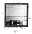
- FIG. 6 shows an enlarged plan view of a pixel according to the present invention.
- FIG. 1 shows a TFT panel 10 used for active matrix display devices, including a matrix of individual AMLCD pixels 20 with their individual NMOS transistors 22 and their individual associated pixel electrodes 24 as used in an AMLCD.
- AMLCD would typically be driven a line at a time.
- Row driver 26 connects through a row conductor 21 the gates 28 of all transistors 22 within a row simultaneously. When gates 28 within a row are turned on, then column driver 30 provides data simultaneously to all the transistors within a row through column conductor 23. Row driver 26 then connects the gates of the next row and the process is repeated, typically at a repetition rate of 60 Hz.
- a body tie buss 25 is represented by the broken line of Fig. 1.
- Body tie buss 25 is electrically connected by 32 to the body of the NMOS transistor at each AMLCD pixel 20 as shown in the enlarged view of a single pixel in Fig. la.
- the body of the NMOS transistors in the row and column drivers are connected to a separate body tie buss (not shown) to which a separate reference voltage or negative power supply will be connected.
- FIG. 2 illustrates the electrical schematic of the AMLCD pixel 22 according to the present invention.
- the liquid crystal pixel is represented by the capacitor 14 (C 1c ).
- the storage capacitor is represented by 16(C s ).
- C s is parallel to C 1c and is defined by the overlap of the body tie buss 25 (TM1) and the pixel electrode 24 (TM2), and the dielectric in between them.
- the body tie buss 25 forms the common electrode of all the pixel storage capacitors.
- the liquid crystal capacitance is defined by the overlap of the pixel electrode (TM2) and the common electrode TM3 on the opposing glass substrate of the LCD structure as shown in Fig. 3.
- FIG. 3 shows a sectional view of one pixel of thin film transistor panel 10 with an NMOS transistor formed on transparent quartz substrate 17 and including source 56, drain 58 and channel 62 regions.
- Row conductor 21 would be connected to gate 28 and column conductor 23 would be connected to source connector contact 27.
- Drain region 58 is connected through contact 59 and tungsten plug 82 to pixel electrode 24 (TM2).
- First transparent metal TM1 is connected to pixel reference voltage region 52 which, through isolation region 60 forms a body tie to channel region 62.
- the present invention preferably utilizes silicon on quartz (SOQ) wafers.
- SOQ silicon on quartz
- AMLCD of the present invention is described as follows. To begin, SOQ wafers with a typical silicon thickness of 3000 angstroms are prepared according to the method of U.S. Patent No. 5,258,323. As shown in Fig. 4a, silicon islands 34 are defined by an island cut mask (Mask #1) and etched. The size of the silicon islands may be anywhere from a centimeter on the side to the size of a single transistor depending upon whether it is in the pixel array region or the row and column driver region. The largest island size to be used is determined by the thermal stress considerations (see U.S. Patent No. 5,258,323). The spacing between the islands is again determined based upon whether it is in the driver area or pixel area.
- Mosk #1 island cut mask
- the spacing between the islands is again determined based upon whether it is in the driver area or pixel area.
- CMOS fabrication After silicon islands 34 and isolation structures 36 have been prepared, one proceeds with the sequence of CMOS fabrication. In the following, the preferred method of fabrication will be described. However, many of the individual steps in the fabrication sequence are conventional.
- the next step is to use the conventional LOCOS (local oxidation process) technique to define device isolation 36 after an oxide growth, a buffered polysilicon layer and a CVD nitride deposition.
- the active MOS region 38 is defined by the field cut (Mask #3). After etching nitride in the field region, field oxide is grown. Then, after stripping the nitride, the polysilicon, and the oxide from the active area. a thin 200 angstrom pad oxide is grown.
- LDD low donor doping
- the p+ regions 48, 50 and 52 are cut (Mask #8), and it is followed by heavy boron implant at the dose level of 2E15 cm -2 at 15 KeV.
- the n+ regions 54, 56 and 58 are cut (Mask #9) and implanted with a heavy phosphorous implant with the dose of 1E15 cm -2 at 30 KeV.
- About 2300 angstroms of oxide layer is CVD deposited and etched to provide spacers 64 ( Figure 4d) to facilitate the silicidation of sources/drains and gate polysilicon with titanium silicide 66 to reduce the resistances.
- TM1 is connected to pixel reference voltage (Vss) at 52.
- Vss pixel reference voltage
- P+ region 52 is connected to channel region 62 by body tie 60 of P- conductivity.
- First transparent metal 72 (TM1) for all pixels 20 are connected together through body tie buss 25 ( Figure 4e). This body tie buss also serves as a pixel storage capacitor buss.
- the transparent metal is deposited and cut (Mask #11)
- another doped oxide layer 74 of 3000 angstrom is then deposited and cut (Mask #12) for making contacts to sources/drains and gates.
- the regular first metal 76 (Metal 1) layer is deposited and defined (Mask #13).
- another doped oxide layer 78 of 5000 angstrom is deposited ( Figure 4f).
- Vias 80 are opened by VIA cut (Mask #14) to provide for the tungsten plug 82 for connecting the first metal 76 to the second transparent metal TM2.
- the tungsten plug 82 is prepared by CVD tungsten deposition followed by planarization.
- second transparent metal TM2 is deposited, patterned and etched (Mask #15). After etching, second transparent metal TM2 defines the pixel electrode 24 of Figure la. Indium Tin Oxide (ITO) is used as a transparent metal.
- ITO Indium Tin Oxide
- FIG.4g shows a schematic cross-section through an assembled display in the region of a pixel.
- the quartz substrate with the active matrix pixel array and the integrated drivers, and the glass substrate with a common electrode 86 (TM3) sandwich a liquid crystal layer that has a typical thickness in the range of 5 microns.
- TM3 common electrode 86
- FIG. 5a shows an silicon island in which N+ source 56 and N+ drain 58 will be formed. Also shown is P+ pixel reference voltage region 52 and P- body tie silicon portion 60 which are interconnected at 61.
- FIG. 5b shows the addition of row conductor 21 which is connected to gate 28.
- FIG. 5c shows connections to source 56 and drain 58. Also shown is first transparent metal 72 (TM1) and its connection to pixel reference voltage or P+ region 52.
- TM1 first transparent metal 72
- FIG. 5d shows column conductor 23 connected to source 56. Also shown is first transparent metal 72 (TM1) which is connected to pixel reference voltage region 52.
- TM1 first transparent metal 72
- FIG. 5e shows regular first metal 76 and tungsten plug 82 connecting first metal 76 to second transparent metal TM2.
- the unique body tie design of the NMOS transistor and the body tie buss will allow a display operating voltage of at least 15 volts for a 2 micron gate length design.
- AMLCD transistor panels have required a light shield to reduce the photoelectric current due to incident light on the transistors which generated electron-hole pairs in the channel region.
- the present invention provides a body tie from the channel region of the NMOS transistor to the pixel reference voltage which allows photocurrents to be extracted from the channel region through the body tie.
- AMLCD's require a pixel storage capacitor.
- a body tie buss 25 which overlaps pixel electrode 24 and is separated from electrode 24 by oxide layers 74 and 78 is shown. The size of body tie buss 25 is selected to provide a desired storage capacitor value.
- AMLCDs of the past have typically had aperture ratios of less than 30%. This is partly due to the light shield requirement.
- the present invention will achieve an aperture ratio of approximately 60% for 2 micron design rules and an aperture ratio greater than 70% for I micron design rules for a display with 25 micron pixel size.
- the high aperture ratio allows use of a lower power backlight and improves the display brightness and efficiency.
- the AMLCDs of the past were often built at low temperatures due to the low temperature process requirements of the conventional transparent substrate.
- the single crystalline silicon film on the high temperature transparent quartz substrate eliminates these limitations and allows normal high temperature silicon processing.
Landscapes
- Liquid Crystal (AREA)
- Thin Film Transistor (AREA)
Claims (7)
- Dünnfilm-Transistorfeld für Aktivmatrix-Flüssigkristall-Anzeigeeinrichtungen AMLCD, aufweisend:wobei das Feld gekennzeichnet ist durch:Ein transparentes isolierendes Substrat (17);mehrere Inseln aus Einkristall-Silicium, die auf dem isolierenden Substrat gebildet und in Reihen und Spalten angeordnet sind;einen NMOS-Transistor, der in jeder Insel gebildet ist und Source-(56), Drain-(58) und Kanalbereiche (62) besitzt, wobei die Source- und Drainbereiche von einem ersten Leitfähigkeitstyp sind, der Transistor eine Gateelektrode (28) an dem Kanalbereich und Source- und Drainelektroden (27,59) besitzt, der Transistor ferner einen Pixel-Referenzpegelbereich (52) eines zweiten Leitfähigkeitstyps besitzt und der zweite Leitfähigkeitstyp entgegengesetzt zu dem ersten Leitfähigkeitstyp ist;mehrere Pixelelektroden (24) im Abstand von den mehreren Transistoren, wobei jede Pixelelektrode an die Drainelektrode eines entsprechenden Transistors angeschlossen ist;mehrere Steuersignalleitungen (23), die gebildet sind, um sich in einer Richtung der Reihen zu erstrecken und die die Gateelektroden der Transistoren in den Reihen verbinden;mehrere Datensignalleitungen (23), die gebildet sind, um sich in einer Richtung der Spalten zu erstrecken und die die Sourceelektroden der Transistoren in den Spalten verbinden:Eine Siliciumkörper-Halteverbindung (60) eines zweiten Leitfähigkeitstyps, die sich von dem Pixel-Referenzspannungsbereich (25,72) zu dem Kanalbereich erstreckt; undeine erste transparente Metallisierung, die sich zu jedem entsprechenden Transistor erstreckt und sich in Kontakt mit jedem Pixel-Referenzspannungsbereich befindet, wobei die erste Metallisierung eine Körper-Halteschiene (25) bildet.
- Feld nach Anspruch 1, dadurch gekennzeichnet,daß die erste transparente Metallisierung (25,72) mehrere erste Bereiche besitzt, jeder erste Bereich durch ein Dielektrikum (74,78) die entsprechende Pixelelektrode (24) überlappt und von dieser beabstandet ist, der erste Bereich eine erste Größe besitzt und die erste Größe ausgewählt ist, um einen ersten Speicherkondensatorwert (16) zu erzielen.
- Feld nach Anspruch 1 oder 2, dadurch gekennzeichnet, daß ein auftreffendes Licht auf den Transistor zu der Erzeugung von Elektronenlochpaaren in dem Kanalbereich führt und die Siliciumverbindung (60) die Elektronenlochpaare herauszieht, wodurch das Erfordernis für eine getrennte Lichtabschirmung der Transistoren vermieden wird.
- Feld nach irgendeinem vorhergehenden Anspruch, dadurch gekennzeichnet, daß der NMOS- Transistor eine Rückschnappspannung von wenigstens 10 V besitzt.
- Feld nach irgendeinem vorhergehenden Anspruch, dadurch gekennzeichnet, daß das AMLCD ein Aperturverhältnis von wenigstens 60 Prozent besitzt.
- Feld nach irgendeinem vorhergehenden Anspruch, g e k e n n z e i c h n e t d u r c h integrierte Einkristall-Siliciumtransistoren hoher Mobilität zur Verwendung als Zeilen- und Spaltentreiber (26,30).
- Verfahren zur Herstellung eines Dünnfilm-Transistorfeldes für eine Aktivmatrix-Flüssigkristall-Anzeigeeinrichtung AMLCD, gekennzeichnet, durch:Vorgabe eines Quarzsubstrates (17);Bildung von Einkristall-Siliciuminseln, die mit den Quarzsubstrat verbunden sind;Isolierung der Siliciuminseln;Bildung eines isolierten Pixel-Referenzspannungsbereiches (52);Siliciumverbindung von Gate, Source- und Drainbereichen;Ablagerung einer ersten Oxydschicht (70);Ätzen der ersten Oxydschicht, um einen Kontakteinschnitt zu dem Referenzspannungsbereich vorzugeben;Ablagerung eines ersten transparenten Metalles (72) für die Verbindung mit dem Referenzspannungsbereich;Ablagerung einer zweiten Oxydschicht (74);Ätzen der zweiten Oxydschicht, um Kontakte zu dem Gate, Source und Drain herzustellen;Ablagerung einer dritten Oxydschicht (78) und Vorsehen von Durchführungen und Verbindungseinrichtungen für die Verbindung mit dem ersten Metall;Ablagerung einer zweiten transparenten Metallschicht; undAusführung von nachfolgenden AMLCD-Montageschritten.
Applications Claiming Priority (3)
| Application Number | Priority Date | Filing Date | Title |
|---|---|---|---|
| US331315 | 1994-10-28 | ||
| US08/331,315 US5536950A (en) | 1994-10-28 | 1994-10-28 | High resolution active matrix LCD cell design |
| PCT/US1995/013688 WO1996013861A1 (en) | 1994-10-28 | 1995-10-16 | High resolution active matrix lcd cell design |
Publications (2)
| Publication Number | Publication Date |
|---|---|
| EP0788657A1 EP0788657A1 (de) | 1997-08-13 |
| EP0788657B1 true EP0788657B1 (de) | 1999-06-02 |
Family
ID=23293446
Family Applications (1)
| Application Number | Title | Priority Date | Filing Date |
|---|---|---|---|
| EP95940542A Expired - Lifetime EP0788657B1 (de) | 1994-10-28 | 1995-10-16 | Zellendesign für hochauflösendes aktiv-matrix-lcd |
Country Status (5)
| Country | Link |
|---|---|
| US (1) | US5536950A (de) |
| EP (1) | EP0788657B1 (de) |
| JP (1) | JPH10508156A (de) |
| DE (1) | DE69510080T2 (de) |
| WO (1) | WO1996013861A1 (de) |
Families Citing this family (39)
| Publication number | Priority date | Publication date | Assignee | Title |
|---|---|---|---|---|
| JPH0943628A (ja) * | 1995-08-01 | 1997-02-14 | Toshiba Corp | 液晶表示装置 |
| US5917563A (en) * | 1995-10-16 | 1999-06-29 | Sharp Kabushiki Kaisha | Liquid crystal display device having an insulation film made of organic material between an additional capacity and a bus line |
| KR0176202B1 (ko) * | 1996-04-09 | 1999-04-15 | 김광호 | 에스.오.아이형 트랜지스터 및 그 제조방법 |
| US6927826B2 (en) * | 1997-03-26 | 2005-08-09 | Semiconductor Energy Labaratory Co., Ltd. | Display device |
| US6197624B1 (en) * | 1997-08-29 | 2001-03-06 | Semiconductor Energy Laboratory Co., Ltd. | Method of adjusting the threshold voltage in an SOI CMOS |
| US7202497B2 (en) * | 1997-11-27 | 2007-04-10 | Semiconductor Energy Laboratory Co., Ltd. | Semiconductor device |
| JP4014710B2 (ja) | 1997-11-28 | 2007-11-28 | 株式会社半導体エネルギー研究所 | 液晶表示装置 |
| US5811855A (en) * | 1997-12-29 | 1998-09-22 | United Technologies Corporation | SOI combination body tie |
| TW486581B (en) * | 1998-01-06 | 2002-05-11 | Seiko Epson Corp | Semiconductor device, substrate for electro-optical device, electro-optical device, electronic equipment, and projection display apparatus |
| JPH11307782A (ja) * | 1998-04-24 | 1999-11-05 | Semiconductor Energy Lab Co Ltd | 半導体装置およびその作製方法 |
| US6278169B1 (en) * | 1998-05-07 | 2001-08-21 | Analog Devices, Inc. | Image sensor shielding |
| US6278502B1 (en) | 1998-09-28 | 2001-08-21 | International Business Machines Corporation | Pixel capacitor formed from multiple layers |
| US6677613B1 (en) * | 1999-03-03 | 2004-01-13 | Semiconductor Energy Laboratory Co., Ltd. | Semiconductor device and method of fabricating the same |
| TW498553B (en) * | 1999-03-11 | 2002-08-11 | Seiko Epson Corp | Active matrix substrate, electro-optical apparatus and method for producing active matrix substrate |
| US6475836B1 (en) | 1999-03-29 | 2002-11-05 | Semiconductor Energy Laboratory Co., Ltd. | Semiconductor device and manufacturing method thereof |
| US7245018B1 (en) * | 1999-06-22 | 2007-07-17 | Semiconductor Energy Laboratory Co., Ltd. | Wiring material, semiconductor device provided with a wiring using the wiring material and method of manufacturing thereof |
| US6133076A (en) * | 1999-08-24 | 2000-10-17 | Semiconductor Energy Laboratory Co., Ltd. | Manufacturing method of semiconductor |
| US6876145B1 (en) * | 1999-09-30 | 2005-04-05 | Semiconductor Energy Laboratory Co., Ltd. | Organic electroluminescent display device |
| TW525216B (en) * | 2000-12-11 | 2003-03-21 | Semiconductor Energy Lab | Semiconductor device, and manufacturing method thereof |
| SG111923A1 (en) | 2000-12-21 | 2005-06-29 | Semiconductor Energy Lab | Light emitting device and method of manufacturing the same |
| JP2002366051A (ja) * | 2001-06-08 | 2002-12-20 | Sanyo Electric Co Ltd | 集積回路チップ及びこれを用いた表示装置 |
| KR100635042B1 (ko) * | 2001-12-14 | 2006-10-17 | 삼성에스디아이 주식회사 | 전면전극을 구비한 평판표시장치 및 그의 제조방법 |
| US7184009B2 (en) * | 2002-06-21 | 2007-02-27 | Nokia Corporation | Display circuit with optical sensor |
| JP4202091B2 (ja) * | 2002-11-05 | 2008-12-24 | 株式会社半導体エネルギー研究所 | アクティブマトリクス型液晶表示装置の作製方法 |
| KR100542986B1 (ko) * | 2003-04-29 | 2006-01-20 | 삼성에스디아이 주식회사 | 박막 트랜지스터, 상기 박막 트랜지스터 제조 방법 및 이를 이용한 표시장치 |
| US7384862B2 (en) | 2003-06-30 | 2008-06-10 | Semiconductor Energy Laboratory Co., Ltd. | Method for fabricating semiconductor device and display device |
| KR100543004B1 (ko) * | 2003-09-18 | 2006-01-20 | 삼성에스디아이 주식회사 | 평판표시장치 |
| KR100541708B1 (ko) * | 2004-02-05 | 2006-01-10 | 매그나칩 반도체 유한회사 | 이미지 센서 및 이의 제조 방법 |
| US7935958B2 (en) * | 2004-10-22 | 2011-05-03 | Semiconductor Energy Laboratory Co., Ltd. | Semiconductor device |
| KR100741976B1 (ko) * | 2005-08-25 | 2007-07-23 | 삼성에스디아이 주식회사 | 박막트랜지스터 및 그 제조 방법 |
| US7514714B2 (en) * | 2006-02-16 | 2009-04-07 | Stmicroelectronics, Inc. | Thin film power MOS transistor, apparatus, and method |
| US7445522B2 (en) * | 2006-12-05 | 2008-11-04 | Tyco Healthcare Group Lp | Electrode connector |
| KR100878284B1 (ko) * | 2007-03-09 | 2009-01-12 | 삼성모바일디스플레이주식회사 | 박막트랜지스터와 그 제조 방법 및 이를 구비한유기전계발광표시장치 |
| US8410554B2 (en) | 2008-03-26 | 2013-04-02 | International Business Machines Corporation | Method, structure and design structure for customizing history effects of SOI circuits |
| US7964467B2 (en) * | 2008-03-26 | 2011-06-21 | International Business Machines Corporation | Method, structure and design structure for customizing history effects of soi circuits |
| US8420460B2 (en) | 2008-03-26 | 2013-04-16 | International Business Machines Corporation | Method, structure and design structure for customizing history effects of SOI circuits |
| GB0811811D0 (en) * | 2008-06-27 | 2008-07-30 | Liquavista Bv | Electrowetting display device |
| US8217456B1 (en) | 2011-03-11 | 2012-07-10 | International Business Machines Corporation | Low capacitance hi-K dual work function metal gate body-contacted field effect transistor |
| KR102446823B1 (ko) * | 2017-06-16 | 2022-09-26 | 삼성디스플레이 주식회사 | 표시 장치 및 그 제조 방법 |
Family Cites Families (18)
| Publication number | Priority date | Publication date | Assignee | Title |
|---|---|---|---|---|
| JPS52124769A (en) * | 1976-04-13 | 1977-10-20 | Matsushita Electric Ind Co Ltd | Suctin tool for electric cleaner |
| GB2223618A (en) * | 1988-10-07 | 1990-04-11 | Philips Electronic Associated | Display devices |
| US5041823A (en) * | 1988-12-29 | 1991-08-20 | Honeywell Inc. | Flicker-free liquid crystal display driver system |
| US5019002A (en) * | 1989-07-12 | 1991-05-28 | Honeywell, Inc. | Method of manufacturing flat panel backplanes including electrostatic discharge prevention and displays made thereby |
| US5191452A (en) * | 1989-09-20 | 1993-03-02 | Honeywell Inc. | Active matrix liquid crystal display fabrication for grayscale |
| US6067062A (en) * | 1990-09-05 | 2000-05-23 | Seiko Instruments Inc. | Light valve device |
| US5162931A (en) * | 1990-11-06 | 1992-11-10 | Honeywell, Inc. | Method of manufacturing flat panel backplanes including redundant gate lines and displays made thereby |
| JP3041947B2 (ja) * | 1990-11-20 | 2000-05-15 | セイコーエプソン株式会社 | 液晶表示装置 |
| US5126865A (en) * | 1990-12-31 | 1992-06-30 | Honeywell Inc. | Liquid crystal display with sub-pixels |
| US5256562A (en) * | 1990-12-31 | 1993-10-26 | Kopin Corporation | Method for manufacturing a semiconductor device using a circuit transfer film |
| CA2061796C (en) * | 1991-03-28 | 2002-12-24 | Kalluri R. Sarma | High mobility integrated drivers for active matrix displays |
| US5110748A (en) * | 1991-03-28 | 1992-05-05 | Honeywell Inc. | Method for fabricating high mobility thin film transistors as integrated drivers for active matrix display |
| JP2900662B2 (ja) * | 1991-10-18 | 1999-06-02 | 三菱電機株式会社 | 薄膜トランジスタアレイ |
| JP2650543B2 (ja) * | 1991-11-25 | 1997-09-03 | カシオ計算機株式会社 | マトリクス回路駆動装置 |
| US5207749A (en) * | 1992-02-13 | 1993-05-04 | Kabushikikaisha Otec | Inner surface shaper |
| TW214603B (en) * | 1992-05-13 | 1993-10-11 | Seiko Electron Co Ltd | Semiconductor device |
| JP3526058B2 (ja) * | 1992-08-19 | 2004-05-10 | セイコーインスツルメンツ株式会社 | 光弁用半導体装置 |
| US5258323A (en) * | 1992-12-29 | 1993-11-02 | Honeywell Inc. | Single crystal silicon on quartz |
-
1994
- 1994-10-28 US US08/331,315 patent/US5536950A/en not_active Expired - Lifetime
-
1995
- 1995-10-16 EP EP95940542A patent/EP0788657B1/de not_active Expired - Lifetime
- 1995-10-16 DE DE69510080T patent/DE69510080T2/de not_active Expired - Lifetime
- 1995-10-16 JP JP8514683A patent/JPH10508156A/ja active Pending
- 1995-10-16 WO PCT/US1995/013688 patent/WO1996013861A1/en not_active Ceased
Also Published As
| Publication number | Publication date |
|---|---|
| DE69510080T2 (de) | 1999-12-16 |
| WO1996013861A1 (en) | 1996-05-09 |
| EP0788657A1 (de) | 1997-08-13 |
| JPH10508156A (ja) | 1998-08-04 |
| DE69510080D1 (de) | 1999-07-08 |
| US5536950A (en) | 1996-07-16 |
Similar Documents
| Publication | Publication Date | Title |
|---|---|---|
| EP0788657B1 (de) | Zellendesign für hochauflösendes aktiv-matrix-lcd | |
| JP3314345B2 (ja) | 高移動度薄膜トランジスタを製造する方法および複数の高移動度薄膜トランジスタ | |
| KR100567145B1 (ko) | 반도체장치및그제조방법 | |
| US7479657B2 (en) | Semiconductor device including active matrix circuit | |
| US6259117B1 (en) | Active matrix display having storage capacitor associated with each pixel transistor | |
| US5110748A (en) | Method for fabricating high mobility thin film transistors as integrated drivers for active matrix display | |
| US6828585B2 (en) | Thin-film transistor, method for fabricating the same, and liquid crystal display device | |
| US7528406B2 (en) | Semiconductor integrated circuit and method of fabricating same | |
| US7109554B2 (en) | Thin film semiconductor device and method for manufacturing same | |
| US5840602A (en) | Methods of forming nonmonocrystalline silicon-on-insulator thin-film transistors | |
| US6028333A (en) | Electric device, matrix device, electro-optical display device, and semiconductor memory having thin-film transistors | |
| US5308779A (en) | Method of making high mobility integrated drivers for active matrix displays | |
| US6847414B2 (en) | Manufacturing method for liquid crystal display | |
| JP2898509B2 (ja) | アクティブマトリックス基板及びその製造方法 | |
| JPH0864830A (ja) | アクティブマトリクス基板およびその製造方法 | |
| US20050218407A1 (en) | Array substrate, liquid crystal display device and method of manufacturing array substrate | |
| JPH09146119A (ja) | 液晶表示装置 | |
| US7115431B2 (en) | Method of fabricating reflective liquid crystal display integrated with driving circuit | |
| US7750349B2 (en) | Switching element substrate, for a liquid crystal display device, including an insulating substrate | |
| JPH08220505A (ja) | 液晶表示装置 | |
| JPH11274512A (ja) | 薄膜トランジスタ装置 | |
| JPH10133226A (ja) | 液晶駆動装置およびその製造方法 |
Legal Events
| Date | Code | Title | Description |
|---|---|---|---|
| PUAI | Public reference made under article 153(3) epc to a published international application that has entered the european phase |
Free format text: ORIGINAL CODE: 0009012 |
|
| 17P | Request for examination filed |
Effective date: 19970424 |
|
| AK | Designated contracting states |
Kind code of ref document: A1 Designated state(s): DE FR GB |
|
| 17Q | First examination report despatched |
Effective date: 19970826 |
|
| GRAG | Despatch of communication of intention to grant |
Free format text: ORIGINAL CODE: EPIDOS AGRA |
|
| GRAG | Despatch of communication of intention to grant |
Free format text: ORIGINAL CODE: EPIDOS AGRA |
|
| GRAH | Despatch of communication of intention to grant a patent |
Free format text: ORIGINAL CODE: EPIDOS IGRA |
|
| GRAH | Despatch of communication of intention to grant a patent |
Free format text: ORIGINAL CODE: EPIDOS IGRA |
|
| GRAA | (expected) grant |
Free format text: ORIGINAL CODE: 0009210 |
|
| AK | Designated contracting states |
Kind code of ref document: B1 Designated state(s): DE FR GB |
|
| REF | Corresponds to: |
Ref document number: 69510080 Country of ref document: DE Date of ref document: 19990708 |
|
| ET | Fr: translation filed | ||
| PLBE | No opposition filed within time limit |
Free format text: ORIGINAL CODE: 0009261 |
|
| STAA | Information on the status of an ep patent application or granted ep patent |
Free format text: STATUS: NO OPPOSITION FILED WITHIN TIME LIMIT |
|
| 26N | No opposition filed | ||
| REG | Reference to a national code |
Ref country code: GB Ref legal event code: IF02 |
|
| PGFP | Annual fee paid to national office [announced via postgrant information from national office to epo] |
Ref country code: GB Payment date: 20090914 Year of fee payment: 15 |
|
| PGFP | Annual fee paid to national office [announced via postgrant information from national office to epo] |
Ref country code: DE Payment date: 20091030 Year of fee payment: 15 |
|
| PGFP | Annual fee paid to national office [announced via postgrant information from national office to epo] |
Ref country code: FR Payment date: 20091020 Year of fee payment: 15 |
|
| GBPC | Gb: european patent ceased through non-payment of renewal fee |
Effective date: 20101016 |
|
| PG25 | Lapsed in a contracting state [announced via postgrant information from national office to epo] |
Ref country code: FR Free format text: LAPSE BECAUSE OF NON-PAYMENT OF DUE FEES Effective date: 20101102 |
|
| REG | Reference to a national code |
Ref country code: FR Ref legal event code: ST Effective date: 20110630 |
|
| REG | Reference to a national code |
Ref country code: DE Ref legal event code: R119 Ref document number: 69510080 Country of ref document: DE Effective date: 20110502 |
|
| PG25 | Lapsed in a contracting state [announced via postgrant information from national office to epo] |
Ref country code: GB Free format text: LAPSE BECAUSE OF NON-PAYMENT OF DUE FEES Effective date: 20101016 |
|
| PG25 | Lapsed in a contracting state [announced via postgrant information from national office to epo] |
Ref country code: DE Free format text: LAPSE BECAUSE OF NON-PAYMENT OF DUE FEES Effective date: 20110502 |
|
| P01 | Opt-out of the competence of the unified patent court (upc) registered |
Effective date: 20230525 |