EP0792092A2 - Procédé de fabrication d'un agencement composite - Google Patents
Procédé de fabrication d'un agencement composite Download PDFInfo
- Publication number
- EP0792092A2 EP0792092A2 EP96117583A EP96117583A EP0792092A2 EP 0792092 A2 EP0792092 A2 EP 0792092A2 EP 96117583 A EP96117583 A EP 96117583A EP 96117583 A EP96117583 A EP 96117583A EP 0792092 A2 EP0792092 A2 EP 0792092A2
- Authority
- EP
- European Patent Office
- Prior art keywords
- recess
- opening
- circuit board
- board substrate
- carrier
- Prior art date
- Legal status (The legal status is an assumption and is not a legal conclusion. Google has not performed a legal analysis and makes no representation as to the accuracy of the status listed.)
- Granted
Links
Images

Classifications
-
- H—ELECTRICITY
- H05—ELECTRIC TECHNIQUES NOT OTHERWISE PROVIDED FOR
- H05K—PRINTED CIRCUITS; CASINGS OR CONSTRUCTIONAL DETAILS OF ELECTRIC APPARATUS; MANUFACTURE OF ASSEMBLAGES OF ELECTRICAL COMPONENTS
- H05K3/00—Apparatus or processes for manufacturing printed circuits
- H05K3/0058—Laminating printed circuit boards onto other substrates, e.g. metallic substrates
- H05K3/0061—Laminating printed circuit boards onto other substrates, e.g. metallic substrates onto a metallic substrate, e.g. a heat sink
-
- H—ELECTRICITY
- H05—ELECTRIC TECHNIQUES NOT OTHERWISE PROVIDED FOR
- H05K—PRINTED CIRCUITS; CASINGS OR CONSTRUCTIONAL DETAILS OF ELECTRIC APPARATUS; MANUFACTURE OF ASSEMBLAGES OF ELECTRICAL COMPONENTS
- H05K3/00—Apparatus or processes for manufacturing printed circuits
- H05K3/30—Assembling printed circuits with electric components, e.g. with resistors
- H05K3/32—Assembling printed circuits with electric components, e.g. with resistors electrically connecting electric components or wires to printed circuits
- H05K3/34—Assembling printed circuits with electric components, e.g. with resistors electrically connecting electric components or wires to printed circuits by soldering
- H05K3/3447—Lead-in-hole components
-
- H—ELECTRICITY
- H05—ELECTRIC TECHNIQUES NOT OTHERWISE PROVIDED FOR
- H05K—PRINTED CIRCUITS; CASINGS OR CONSTRUCTIONAL DETAILS OF ELECTRIC APPARATUS; MANUFACTURE OF ASSEMBLAGES OF ELECTRICAL COMPONENTS
- H05K2201/00—Indexing scheme relating to printed circuits covered by H05K1/00
- H05K2201/03—Conductive materials
- H05K2201/0332—Structure of the conductor
- H05K2201/0364—Conductor shape
- H05K2201/0367—Metallic bump or raised conductor not used as solder bump
-
- H—ELECTRICITY
- H05—ELECTRIC TECHNIQUES NOT OTHERWISE PROVIDED FOR
- H05K—PRINTED CIRCUITS; CASINGS OR CONSTRUCTIONAL DETAILS OF ELECTRIC APPARATUS; MANUFACTURE OF ASSEMBLAGES OF ELECTRICAL COMPONENTS
- H05K2201/00—Indexing scheme relating to printed circuits covered by H05K1/00
- H05K2201/09—Shape and layout
- H05K2201/09009—Substrate related
- H05K2201/09036—Recesses or grooves in insulating substrate
-
- H—ELECTRICITY
- H05—ELECTRIC TECHNIQUES NOT OTHERWISE PROVIDED FOR
- H05K—PRINTED CIRCUITS; CASINGS OR CONSTRUCTIONAL DETAILS OF ELECTRIC APPARATUS; MANUFACTURE OF ASSEMBLAGES OF ELECTRICAL COMPONENTS
- H05K2201/00—Indexing scheme relating to printed circuits covered by H05K1/00
- H05K2201/09—Shape and layout
- H05K2201/09009—Substrate related
- H05K2201/09063—Holes or slots in insulating substrate not used for electrical connections
-
- H—ELECTRICITY
- H05—ELECTRIC TECHNIQUES NOT OTHERWISE PROVIDED FOR
- H05K—PRINTED CIRCUITS; CASINGS OR CONSTRUCTIONAL DETAILS OF ELECTRIC APPARATUS; MANUFACTURE OF ASSEMBLAGES OF ELECTRICAL COMPONENTS
- H05K2201/00—Indexing scheme relating to printed circuits covered by H05K1/00
- H05K2201/10—Details of components or other objects attached to or integrated in a printed circuit board
- H05K2201/10613—Details of electrical connections of non-printed components, e.g. special leads
- H05K2201/10742—Details of leads
- H05K2201/10886—Other details
- H05K2201/10901—Lead partly inserted in hole or via
-
- H—ELECTRICITY
- H05—ELECTRIC TECHNIQUES NOT OTHERWISE PROVIDED FOR
- H05K—PRINTED CIRCUITS; CASINGS OR CONSTRUCTIONAL DETAILS OF ELECTRIC APPARATUS; MANUFACTURE OF ASSEMBLAGES OF ELECTRICAL COMPONENTS
- H05K2203/00—Indexing scheme relating to apparatus or processes for manufacturing printed circuits covered by H05K3/00
- H05K2203/11—Treatments characterised by their effect, e.g. heating, cooling, roughening
- H05K2203/1178—Means for venting or for letting gases escape
-
- H—ELECTRICITY
- H05—ELECTRIC TECHNIQUES NOT OTHERWISE PROVIDED FOR
- H05K—PRINTED CIRCUITS; CASINGS OR CONSTRUCTIONAL DETAILS OF ELECTRIC APPARATUS; MANUFACTURE OF ASSEMBLAGES OF ELECTRICAL COMPONENTS
- H05K2203/00—Indexing scheme relating to apparatus or processes for manufacturing printed circuits covered by H05K3/00
- H05K2203/13—Moulding and encapsulation; Deposition techniques; Protective layers
- H05K2203/1377—Protective layers
- H05K2203/1394—Covering open PTHs, e.g. by dry film resist or by metal disc
-
- H—ELECTRICITY
- H05—ELECTRIC TECHNIQUES NOT OTHERWISE PROVIDED FOR
- H05K—PRINTED CIRCUITS; CASINGS OR CONSTRUCTIONAL DETAILS OF ELECTRIC APPARATUS; MANUFACTURE OF ASSEMBLAGES OF ELECTRICAL COMPONENTS
- H05K3/00—Apparatus or processes for manufacturing printed circuits
- H05K3/0094—Filling or covering plated through-holes or blind plated vias, e.g. for masking or for mechanical reinforcement
-
- Y—GENERAL TAGGING OF NEW TECHNOLOGICAL DEVELOPMENTS; GENERAL TAGGING OF CROSS-SECTIONAL TECHNOLOGIES SPANNING OVER SEVERAL SECTIONS OF THE IPC; TECHNICAL SUBJECTS COVERED BY FORMER USPC CROSS-REFERENCE ART COLLECTIONS [XRACs] AND DIGESTS
- Y10—TECHNICAL SUBJECTS COVERED BY FORMER USPC
- Y10T—TECHNICAL SUBJECTS COVERED BY FORMER US CLASSIFICATION
- Y10T156/00—Adhesive bonding and miscellaneous chemical manufacture
- Y10T156/16—Surface bonding means and/or assembly means with bond interfering means [slip sheet, etc. ]
Definitions
- the invention relates to a method for producing a composite arrangement, wherein at least one printed circuit board substrate is connected to a carrier under the action of a pressure exerted by a press ram via a resin layer impregnated with fabric (prepreg).
- a method for connecting circuit arrangements equipped with electronic components, for example printed circuit boards or hybrid elements, to a carrier is described, for example, in DE 42 40 996 C1.
- the circuit arrangements are glued flat on the carrier by means of an adhesive.
- the disadvantage of this method is that the resin liquefying during the pressing process is undefined in bores, vias and the like. Like.
- the circuit board substrate flows and thereby the holes, vias and the like. for later processing of the circuit board, e.g. for soldering connection legs of components on the circuit board, partially or completely closed. In extreme cases, this means that the circuit board cannot be processed further.
- the invention is therefore based on the object to improve a method for producing a composite arrangement of the generic type in such a way that when connecting the circuit board substrate to the carrier no resin undefined in bores, vias and the like. can flow.
- This object is achieved according to the invention in a method for producing a composite arrangement of the type described in the introduction in that the pressing pressure is at least partially reduced in the region of an opening in the circuit board substrate.
- the partial or complete reduction i.e. Removal of the pressing pressure in the area of an opening of the circuit board substrate, for example in the area of a hole or a via, has the great advantage that the resin in this area flows less strongly or not at all because of the reduced or completely removed pressing pressure, so that there is also no undefined flow in the openings in this area, ie Holes or vias.
- An advantageous embodiment consists in providing a recess in the carrier in the region of the opening and a connection of the recess with the surroundings.
- the printed circuit board substrate is applied to the printed circuit board with a lower pressing pressure during the production of the composite arrangement, ie the printed circuit board assembly.
- This easily prevents the circuit board substrate from sticking to the carrier in the region of the opening. In this way, no resin can flow in the area of the opening and flow into the opening.
- the connection with the environment is particularly important with regard to a later soldering process (reflow soldering) at a high temperature necessary.
- the air enclosed in the recess between the circuit board substrate and the carrier expands. This heated air can advantageously escape into the atmosphere through the connection.
- connection itself can be established in a wide variety of ways.
- a hole in the carrier would be conceivable as a connection.
- a ventilation hole arranged in the circuit board substrate and in the prepreg is particularly advantageous.
- Another, particularly advantageous implementation of the method provides that the press ram has a recess in the area of the opening.
- a press insert is placed between the press ram and the circuit board substrate and has a recess in the area of the opening. This recess in the press insert also substantially or completely reduces the pressure exerted on the substrate and thus on the prepreg and the carrier.
- the recess arranged in the base plate is advantageously on the tolerances of the circuit board substrate and to the connector pins, connecting wires and the like to be arranged in the opening. customized.
- Another particularly advantageous embodiment of the method uses a press die which has a recess in the area of the opening and additionally a recess in the base plate in the area of the opening, adapted to the recess in the press die and a connection of the recess to the surroundings. This arrangement completely suppresses the exertion of a pressing pressure in the region of the opening.
- a further, particularly advantageous embodiment of the method provides that a press insert is placed between the press ram and the circuit board substrate and that in addition in the base plate in the region of the opening there is a recess adapted to the recess in the press insert and a connection of the recess with the Environment is provided. Also through this Arrangement, the pressure in the area of the opening is suppressed particularly effectively.
- a recess is also provided in the prepreg in the area of the opening. This practically completely suppresses the pressure in the area of the opening.
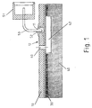
- a composite arrangement is produced in that a circuit board substrate 10 under the influence of a pressure p exerted by a press ram 20 via a resin-impregnated one Fabric layer, a so-called prepreg 30, is connected to a carrier 40. At the same time as the pressing pressure p is exerted, heat can be supplied via the press ram 20.
- the resin flows in the prepreg 30 and thereby creates an adhesive connection between the circuit board substrate 10 and the carrier 40, which usually consists of a metal, for example aluminum.
- the method is not limited to the application of a printed circuit board substrate 10 to a carrier 40, but rather that in this way a plurality of printed circuit board substrates 10 can also be fastened one above the other on a carrier 40 via a prepreg 30.
- the pressing pressure p is reduced or completely removed in the region 12 of the opening 11. This is done, for example, in that a recess 42 is provided in the carrier 40, so that a lower pressing pressure p is exerted in this area via the press die 20, since the press die 20 in this area in addition to the circuit board substrate 10 and the prepreg 30 does not Facing printing area (see. In particular Fig. 1).
- a contact element for example a connecting wire 50 of a plug 51, is connected to the printed circuit board substrate 10 by means of reflow soldering by means of a solder connection 52 in a later method step.
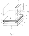
- the pressure p on the printed circuit board substrate 10 in the area 12 of the opening 11 can also be reduced in that the ram 70 has a recess 71 in the area 12 of the opening 11, as is shown schematically in FIG. 2. This also avoids that a pressure p is exerted on the circuit board substrate 10 and via this on the prepreg 30 and as a result the resin flows into the opening 11, clogs it and makes it inaccessible for later processing.
- a press insert 80 can be placed between the press die 70 and the printed circuit board substrate 10 and has a recess 81 in the area 12 of the opening 11. This recess 81 arranged in the press insert 80 also prevents a pressure p being exerted on the printed circuit board substrate 10 in the region 12 of the opening 11, which leads to an undesirable flow of the resin.
- a recess (not shown) can be provided in the prepreg 30 in the region 12 of the opening 11.
- the recess 42 arranged in the carrier 40 is based on the tolerances of the circuit board substrate 10 and the tolerances of the plug pins, connecting wires 50 and the like to be arranged in the opening 11. customized.
- a particularly effective embodiment of the method is that the ram 70 has a recess 71 in the area of the opening and that in the carrier 40 in the area 12 of the opening 11 there is a recess 43 in the carrier 40 that is adapted to the recess 71 in the ram 70 and a connection of this recess 43 to the surroundings in the form of a vent hole 60 is provided (see FIG. 2).
- the press insert 80 which has the recess 81 in the area of the opening 11, is placed between the press die 70 and the circuit board substrate 10, and that in addition to this, in the base plate in the area 12 the opening 11 has a recess 44 which is adapted to the recess 81 in the press insert 80, and a connection of the recess 44 to the surroundings in the form of the vent hole 60 is provided.
- a recess (not shown) can also be provided in the prepreg 30, which is adapted to the corresponding recesses 43, 44 in the carrier 40 and to the recess 71 in the press ram 70 or to the recess 81 in the press insert 80.
Landscapes
- Engineering & Computer Science (AREA)
- Manufacturing & Machinery (AREA)
- Microelectronics & Electronic Packaging (AREA)
- Production Of Multi-Layered Print Wiring Board (AREA)
- Casting Or Compression Moulding Of Plastics Or The Like (AREA)
Applications Claiming Priority (2)
| Application Number | Priority Date | Filing Date | Title |
|---|---|---|---|
| DE19607014A DE19607014A1 (de) | 1996-02-24 | 1996-02-24 | Verfahren zur Herstellung einer Verbundanordnung |
| DE19607014 | 1996-02-24 |
Publications (3)
| Publication Number | Publication Date |
|---|---|
| EP0792092A2 true EP0792092A2 (fr) | 1997-08-27 |
| EP0792092A3 EP0792092A3 (fr) | 1998-07-29 |
| EP0792092B1 EP0792092B1 (fr) | 2007-12-12 |
Family
ID=7786360
Family Applications (1)
| Application Number | Title | Priority Date | Filing Date |
|---|---|---|---|
| EP96117583A Expired - Lifetime EP0792092B1 (fr) | 1996-02-24 | 1996-11-02 | Procédé de fabrication d'un agencement composite |
Country Status (4)
| Country | Link |
|---|---|
| US (1) | US5925210A (fr) |
| EP (1) | EP0792092B1 (fr) |
| JP (1) | JP3943181B2 (fr) |
| DE (2) | DE19607014A1 (fr) |
Cited By (1)
| Publication number | Priority date | Publication date | Assignee | Title |
|---|---|---|---|---|
| FR2779900A1 (fr) * | 1998-06-10 | 1999-12-17 | Siemens Ag | Agencement de circuit electrique multicouche |
Families Citing this family (7)
| Publication number | Priority date | Publication date | Assignee | Title |
|---|---|---|---|---|
| KR100254323B1 (ko) * | 1997-08-01 | 2000-05-01 | 윤종용 | 집적회로 납땜 장치 및 방법 |
| US6663442B1 (en) | 2000-01-27 | 2003-12-16 | Tyco Electronics Corporation | High speed interconnect using printed circuit board with plated bores |
| DE10026270C1 (de) * | 2000-05-26 | 2001-12-20 | Siemens Ag | Verfahren zum Laminieren einer Leiterplatte auf eine Grundplatte und Laminiervorrichtung |
| ITMO20030200A1 (it) * | 2003-07-10 | 2005-01-11 | Nuova Laelvi S R L | Procedimento di assemblaggio di un circuito stampato |
| US20140093643A1 (en) * | 2012-09-28 | 2014-04-03 | Tyco Electronics Services Gmbh | Method and system of depositing a viscous material into a surface cavity |
| TWI546000B (zh) | 2012-10-02 | 2016-08-11 | 健鼎科技股份有限公司 | 電路板封裝結構及其製造方法 |
| CN105263261B (zh) * | 2015-09-30 | 2018-12-25 | 景旺电子科技(龙川)有限公司 | 一种封闭式金属基绝缘槽的制作方法 |
Citations (1)
| Publication number | Priority date | Publication date | Assignee | Title |
|---|---|---|---|---|
| DE4240996C1 (de) | 1992-12-05 | 1994-06-16 | Bosch Gmbh Robert | Verfahren zur Herstellung einer Verbundanordnung |
Family Cites Families (7)
| Publication number | Priority date | Publication date | Assignee | Title |
|---|---|---|---|---|
| US2495761A (en) * | 1944-10-19 | 1950-01-31 | Chicopee Mfg Corp Of Georgia | Method of splicing sheet material |
| US3158927A (en) * | 1961-06-05 | 1964-12-01 | Burroughs Corp | Method of fabricating sub-miniature semiconductor matrix apparatus |
| JPS60149196A (ja) * | 1984-01-17 | 1985-08-06 | ソニー株式会社 | プリント基板およびその製造方法 |
| JPH0456187A (ja) * | 1990-06-21 | 1992-02-24 | Mitsubishi Electric Corp | プリント配線板の製造方法 |
| JPH04206675A (ja) * | 1990-11-30 | 1992-07-28 | Nippon Avionics Co Ltd | ヒートシンク付きプリント配線板 |
| JPH04296084A (ja) * | 1991-03-25 | 1992-10-20 | Yamashita Saakitetsuku Kk | 放熱板裏張り型プリント配線板 |
| DE4307134C2 (de) * | 1993-03-06 | 2002-04-04 | Bosch Gmbh Robert | Steckerleiste für elektronische Steuergeräte in Kraftfahrzeugen |
-
1996
- 1996-02-24 DE DE19607014A patent/DE19607014A1/de not_active Ceased
- 1996-11-02 DE DE59611454T patent/DE59611454D1/de not_active Expired - Lifetime
- 1996-11-02 EP EP96117583A patent/EP0792092B1/fr not_active Expired - Lifetime
-
1997
- 1997-02-20 JP JP03540097A patent/JP3943181B2/ja not_active Expired - Fee Related
- 1997-02-21 US US08/803,654 patent/US5925210A/en not_active Expired - Lifetime
Patent Citations (1)
| Publication number | Priority date | Publication date | Assignee | Title |
|---|---|---|---|---|
| DE4240996C1 (de) | 1992-12-05 | 1994-06-16 | Bosch Gmbh Robert | Verfahren zur Herstellung einer Verbundanordnung |
Cited By (1)
| Publication number | Priority date | Publication date | Assignee | Title |
|---|---|---|---|---|
| FR2779900A1 (fr) * | 1998-06-10 | 1999-12-17 | Siemens Ag | Agencement de circuit electrique multicouche |
Also Published As
| Publication number | Publication date |
|---|---|
| DE59611454D1 (de) | 2008-01-24 |
| US5925210A (en) | 1999-07-20 |
| EP0792092B1 (fr) | 2007-12-12 |
| EP0792092A3 (fr) | 1998-07-29 |
| JPH09237954A (ja) | 1997-09-09 |
| JP3943181B2 (ja) | 2007-07-11 |
| DE19607014A1 (de) | 1997-08-28 |
Similar Documents
| Publication | Publication Date | Title |
|---|---|---|
| DE102004019567B3 (de) | Verfahren zur Befestigung von elektronischen Bauelementen auf einem Substrat | |
| EP2566308B1 (fr) | Procédé d'équipement d'une plaquette | |
| DE19600928A1 (de) | Vorrichtung zur Handhabung von Leiterplatten und deren Herstellung | |
| EP0792092A2 (fr) | Procédé de fabrication d'un agencement composite | |
| EP1665914A1 (fr) | Carte de circuits imprimes comprenant un dispositif de maintien concu pour maintenir des composants electroniques cables, procede pour produire une telle carte de circuits imprimes et son utilisation dans un four a braser | |
| EP1420997A1 (fr) | Ensemble de vehicule automobile | |
| EP1352551B1 (fr) | Procede et dispositif pour placer des fils conducteurs sur ou dans une couche de support | |
| DE3318717C1 (de) | Verfahren zum Herstellen von Leiterplatten mit starren und flexiblen Bereichen | |
| EP0613331A1 (fr) | Méthode d'attachement d'un circuit hybride sur un circuit imprimé | |
| DE102016220678A1 (de) | Druckvorrichtung und Druckverfahren zum Auftragen eines viskosen oder pastösen Materials | |
| DE102006056793B4 (de) | Elektronikvorrichtung und Verfahren zum Herstellen derselben | |
| DE19852832A1 (de) | Verfahren zur Herstellung eines Metall-Kunststoff-Laminats | |
| DE69803664T2 (de) | Verfahren zur herstellung von gedruckten leiterplatten und so hergestellte gedruckte leiterplatten | |
| EP3645189B1 (fr) | Procédé de fabrication d'une pièce composite en acier ainsi que pièce composite en acier | |
| EP0751562B1 (fr) | Fixation thermiquement conductive d'un dispositif électronique de puissance sur une plaquette de circuit avec dissipateur de chaleur | |
| DE60130108T2 (de) | Verfahren zur herstellung elektrischer verbindungselemente und verbindungselement | |
| DE102018203718A1 (de) | Spannmittel, Spanneinrichtung mit Spannmitteln sowie Spannvorrichtung | |
| DE102009039377B4 (de) | Leiterplattenmodul und zugehöriges Herstellungsverfahren | |
| DE4208594A1 (de) | Verfahren zur herstellung einer elektrischen, vorgefertigten baueinheit und deren befestigung auf einer leiterplatte | |
| EP3476574B1 (fr) | Procédé d'alignement et de collage de deux composants au moyen d'un adhésif à deux composants et dispositif | |
| DE102005017002A1 (de) | Verfahren zur Herstellung einer räumlichen, wenigstens in einem Teilbereich gekrümmten Leiterplatte sowie nach diesem Verfahren hergestellte Leiterplatte | |
| DE19533251A1 (de) | Verfahren zur wärmeleitenden Befestigung eines elektronischen Leistungsbauelementes auf einer Leiterplatte mit einem Kühlblech oder Kühlkörper | |
| DE102023204543A1 (de) | Bauteilanordnung sowie Werkzeug und Verfahren zur Herstellung einer solchen Bauteilanordnung | |
| DE102022131477A1 (de) | Verfahren zur Applikation eines pastösen Materials sowie Fahrzeug | |
| EP1113712B1 (fr) | Procédé de fabrication de lignes conductrices |
Legal Events
| Date | Code | Title | Description |
|---|---|---|---|
| PUAI | Public reference made under article 153(3) epc to a published international application that has entered the european phase |
Free format text: ORIGINAL CODE: 0009012 |
|
| AK | Designated contracting states |
Kind code of ref document: A2 Designated state(s): DE FR GB IT |
|
| PUAL | Search report despatched |
Free format text: ORIGINAL CODE: 0009013 |
|
| AK | Designated contracting states |
Kind code of ref document: A3 Designated state(s): DE FR GB IT |
|
| 17P | Request for examination filed |
Effective date: 19990129 |
|
| 17Q | First examination report despatched |
Effective date: 20060117 |
|
| GRAP | Despatch of communication of intention to grant a patent |
Free format text: ORIGINAL CODE: EPIDOSNIGR1 |
|
| GRAS | Grant fee paid |
Free format text: ORIGINAL CODE: EPIDOSNIGR3 |
|
| GRAA | (expected) grant |
Free format text: ORIGINAL CODE: 0009210 |
|
| AK | Designated contracting states |
Kind code of ref document: B1 Designated state(s): DE FR GB IT |
|
| REG | Reference to a national code |
Ref country code: GB Ref legal event code: FG4D Free format text: NOT ENGLISH |
|
| REF | Corresponds to: |
Ref document number: 59611454 Country of ref document: DE Date of ref document: 20080124 Kind code of ref document: P |
|
| GBT | Gb: translation of ep patent filed (gb section 77(6)(a)/1977) |
Effective date: 20080319 |
|
| ET | Fr: translation filed | ||
| PLBE | No opposition filed within time limit |
Free format text: ORIGINAL CODE: 0009261 |
|
| STAA | Information on the status of an ep patent application or granted ep patent |
Free format text: STATUS: NO OPPOSITION FILED WITHIN TIME LIMIT |
|
| 26N | No opposition filed |
Effective date: 20080915 |
|
| PGFP | Annual fee paid to national office [announced via postgrant information from national office to epo] |
Ref country code: FR Payment date: 20101130 Year of fee payment: 15 |
|
| PGFP | Annual fee paid to national office [announced via postgrant information from national office to epo] |
Ref country code: IT Payment date: 20101124 Year of fee payment: 15 Ref country code: GB Payment date: 20101123 Year of fee payment: 15 |
|
| PGFP | Annual fee paid to national office [announced via postgrant information from national office to epo] |
Ref country code: DE Payment date: 20110125 Year of fee payment: 15 |
|
| GBPC | Gb: european patent ceased through non-payment of renewal fee |
Effective date: 20111102 |
|
| REG | Reference to a national code |
Ref country code: FR Ref legal event code: ST Effective date: 20120731 |
|
| PG25 | Lapsed in a contracting state [announced via postgrant information from national office to epo] |
Ref country code: IT Free format text: LAPSE BECAUSE OF NON-PAYMENT OF DUE FEES Effective date: 20111102 |
|
| REG | Reference to a national code |
Ref country code: DE Ref legal event code: R119 Ref document number: 59611454 Country of ref document: DE Effective date: 20120601 |
|
| PG25 | Lapsed in a contracting state [announced via postgrant information from national office to epo] |
Ref country code: GB Free format text: LAPSE BECAUSE OF NON-PAYMENT OF DUE FEES Effective date: 20111102 |
|
| PG25 | Lapsed in a contracting state [announced via postgrant information from national office to epo] |
Ref country code: FR Free format text: LAPSE BECAUSE OF NON-PAYMENT OF DUE FEES Effective date: 20111130 |
|
| PG25 | Lapsed in a contracting state [announced via postgrant information from national office to epo] |
Ref country code: DE Free format text: LAPSE BECAUSE OF NON-PAYMENT OF DUE FEES Effective date: 20120601 |