EP0793247B1 - Geräuscharme Dispersionselektrolumineszenzvorrichtung, und Schalter der diese verwendet - Google Patents
Geräuscharme Dispersionselektrolumineszenzvorrichtung, und Schalter der diese verwendet Download PDFInfo
- Publication number
- EP0793247B1 EP0793247B1 EP97103288A EP97103288A EP0793247B1 EP 0793247 B1 EP0793247 B1 EP 0793247B1 EP 97103288 A EP97103288 A EP 97103288A EP 97103288 A EP97103288 A EP 97103288A EP 0793247 B1 EP0793247 B1 EP 0793247B1
- Authority
- EP
- European Patent Office
- Prior art keywords
- layer
- electrode layer
- electroluminescent device
- insulating
- insulating substrate
- Prior art date
- Legal status (The legal status is an assumption and is not a legal conclusion. Google has not performed a legal analysis and makes no representation as to the accuracy of the status listed.)
- Expired - Lifetime
Links
Images






Classifications
-
- H—ELECTRICITY
- H01—ELECTRIC ELEMENTS
- H01H—ELECTRIC SWITCHES; RELAYS; SELECTORS; EMERGENCY PROTECTIVE DEVICES
- H01H13/00—Switches having rectilinearly-movable operating part or parts adapted for pushing or pulling in one direction only, e.g. push-button switch
- H01H13/70—Switches having rectilinearly-movable operating part or parts adapted for pushing or pulling in one direction only, e.g. push-button switch having a plurality of operating members associated with different sets of contacts, e.g. keyboard
- H01H13/702—Switches having rectilinearly-movable operating part or parts adapted for pushing or pulling in one direction only, e.g. push-button switch having a plurality of operating members associated with different sets of contacts, e.g. keyboard with contacts carried by or formed from layers in a multilayer structure, e.g. membrane switches
-
- H—ELECTRICITY
- H05—ELECTRIC TECHNIQUES NOT OTHERWISE PROVIDED FOR
- H05B—ELECTRIC HEATING; ELECTRIC LIGHT SOURCES NOT OTHERWISE PROVIDED FOR; CIRCUIT ARRANGEMENTS FOR ELECTRIC LIGHT SOURCES, IN GENERAL
- H05B33/00—Electroluminescent light sources
- H05B33/12—Light sources with substantially two-dimensional [2D] radiating surfaces
-
- H—ELECTRICITY
- H01—ELECTRIC ELEMENTS
- H01H—ELECTRIC SWITCHES; RELAYS; SELECTORS; EMERGENCY PROTECTIVE DEVICES
- H01H2219/00—Legends
- H01H2219/002—Legends replaceable; adaptable
- H01H2219/018—Electroluminescent panel
-
- H—ELECTRICITY
- H01—ELECTRIC ELEMENTS
- H01H—ELECTRIC SWITCHES; RELAYS; SELECTORS; EMERGENCY PROTECTIVE DEVICES
- H01H2239/00—Miscellaneous
- H01H2239/004—High frequency adaptation or shielding
Definitions
- the present invention relates generally to a noiseless dispersion electroluminescent device which may be employed in illumination of an input unit of a variety of electronic equipment and a switch unit using the same.
- Fig. 10 shows a conventional dispersion electroluminescent (EL) device.
- Fig. 11 shows a conventional illuminated switch unit using the EL device.
- the EL device 1 in Fig. 10 includes a laminated multi-layer having a thickness of approximately 0.3mm consisting of an insulating substrate 2 made of a transparent resin film of approximately 100 ⁇ m thick, a transparent electrode layer 3, a luminescent layer 4, a dielectric layer 5, a back electrode layer 6, and an insulating layer 7.
- the switch unit 8 as shown in Fig. 11, includes a membrane switch 14, the EL device 1, a spacer 18, and a front sheet 17.
- the membrane switch 14 includes an upper insulating plate 9, a spacer 13, and a lower insulating plate 11.
- the upper insulating plate 13 is made of a resin film having a thickness of approximately 100 ⁇ m and has printed on its back surface moving contacts 10.
- the lower insulating plate 11 is made of a resin film and has printed on its front surface stationary contacts 12. The moving contacts 10 and the stationary contacts 12 are separated at a given gap through the spacer 13 secured between the upper and lower insulating plates 9 and 11 with adhesive.
- the EL device 1 is disposed on the membrane switch 14.
- the front sheet 17 made of a transparent resin film is disposed on the EL device 1 through the spacer 13 whose both surfaces are applied with adhesive.
- Push buttons 15 made with a transparent or semitransparent resin casting are attached to the back surface of the front sheet 17 through an adhesive member 16.
- the switch unit 18 is turned on by depressing the push button 15 through the front sheet 17 to press a portion of the EL device 1 so that the moving contacts 10 attached to the upper insulating plate 9 are brought into contact with the stationary contacts 12 attached to the lower insulating plate 11.
- the above EL device 1 and the switching unit 8 however have the following drawback.
- the ac voltage or dc pulse voltage is applied across the transparent electrode layer 3 and the back electrode layer 6 to activate the EL device 1, it will cause the EL device 1 to produce mechanical vibrations due to the piezoelectric effect of barium titanate (BaTiO 3 ) contained in the luminescent layer 4 and the dielectric layer 5. which are in turn, transmitted as noise through a structure in contact with the EL device 1 to an operator and which may interfere with radio communication, for example, in a portable telephone or a cordless telephone, leading to difficulty in hearing voice from a calling party.
- barium titanate BaTiO 3
- the switching unit 8 also has the disadvantage that nonuniform light may emerge from the front sheet 17 of the EL device 1 due to partial deformation of the push button 15 and the spacer 18 when depressed to turn on the switching unit 8.
- a total thickness of the EL device 1 and the upper insulating plate 9 of the membrane switch 14 is as much as approximately 0.4mm, therefore, much depression force is required to flex the EL device 1 and the upper insulating plate 9 to make contact between the moving contacts 10 and the stationary contacts 12.
- increasing a flexible area results in an increased overall size of the switch unit 8. Further, it is difficult to thin the switching unit 8 because of complexity of the structure.
- a noiseless and compact electroluminescent device designed to provide uniform illumination and a switching unit using the same are provided.
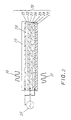
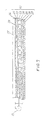
- a dispersion electroluminescent (EL) device 28 according to the first embodiment of the invention.
- the EL device 28 has a total thickness of approximately 0.3mm and includes an upper insulating substrate 19, a transparent electrode layer 20, an electroluminescent layer 21, a first dielectric layer 22, a first back electrode layer 23, a first insulating layer 24, a second dielectric layer 25, a second back electrode layer 26, and a second insulating layer 27.
- the upper insulating substrate 19 is made of an elastic transparent resin film having a thickness of approximately 80 ⁇ m.
- the transparent electrode layer 20 is printed on a lower surface of the upper insulating substrate 19 using a dispersion transparent paste made of a transparent insulating resin over which an indium oxide powder is distributed finely.
- the electroluminescent layer 21 is printed or formed on a lower surface of the transparent electrode layer 20 using a binder resin paste over which a zinc sulfide fluorescent powder is stirred and distributed.
- the first dielectric layer 22 is printed on the lower surface of the electroluminescent layer 21 using a binder resin paste over which a barium titanate powder is stirred and distributed.
- the first back electrode layer 23 is printed on a lower surface of the first dielectric layer 22 using a carbon resin paste.
- the first insulating layer 24 is printed on a lower surface of the first back electrode layer 23 using vinyl acetate-vinyl chloride copolymer insulating resist (hereinafter, referred to as an insulating resist).
- the second dielectric layer 25 is printed on a lower surface of the first insulating layer 24 using a binder resin paste over which a barium titanate powder is stirred and distributed.
- the second back electrode layer 26 is printed on a lower surface of the second dielectric layer 25 using a carbon resin paste.
- the second insulating layer 27 is printed on a lower surface of the second back electrode layer 26 using the insulating resist.
- the first back electrode layer 23 serves as a common electrode.
- the application of ac voltages, which are 180° out of phase with each other, across the first back electrode layer 23 and the transparent electrode layer 20 and across the first back electrode layer 23 and the second back electrode layer 26 through a driver circuit 29 causes the EL device 28 to emit light through the upper insulating substrate 19.
- the application of the ac voltages to the transparent electrode layer 20 and the second back electrode layer 26 will induce, as discussed in the introductory part of this application, the piezoelectric effect of barium titanate contained in the luminescent layer 21, the first dielectric layer 22, and the second dielectric layer 25.
- the piezoelectric effect in the luminescent layer 21 and the first dielectric layer 22 causes a mechanical vibration 30 to be produced.
- the piezoelectric effect in the second dielectric layer 25 causes a mechanical vibration 31 to be produced.
- the mechanical vibration 30 is, as clearly shown in the drawing, 180° out of phase with the mechanical vibration 31, so that they are canceled by one another to reduce the level of sound pressure generated from the EL device 28. This realizes a noiseless EL device.
- the EL device 28 is, as described above, 0.3mm in thickness and provides good flexibility when used with a switch unit.
- the above described vibration reduction effect of the EL device 28 may also be achieved by using dc pulse voltages instead of the ac voltages provided by the drive circuit 29.
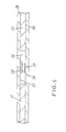
- Fig. 3 shows an illuminated switch unit 32 according to the second embodiment which uses the EL device 28 as shown in Figs. 1 and 2.
- the switch unit 32 also includes a spacer 37, a moving contact 33, a stationary contact 35, and a lower insulating substrate 34.
- the moving contact 33 is printed on a lower surface of the second insulating layer 27 of the EL device 28 using a conductive paste such as a silver or carbon resin paste.
- the stationary contact 35 is printed on an upper surface of the lower insulating substrate 34.
- the spacer 37 is formed with a resin film having applied on its both surfaces adhesive and bonds the EL device 28 and the lower insulating substrate 34 together.
- the spacer 37 has an opening 36 which expose the moving contact 33 to the stationary contact 35 at a given interval away from each other.
- depressing a portion of the upper surface of the EL device 28 opposed to the moving contact 33 causes the moving contact 33 to be brought into contact with the stationary contact 35 to establish electric communication therebetween.
- the structure of the switch unit 32 eliminates the need for a member disturbing light transmission to be disposed on the EL device 28, thus resulting in uniform illumination through the EL device 28.
- the EL device 28 is, as described above, 0.3mm in thickness and provides good flexibility allowing the moving and stationary contacts 33 and 35 to make contact with a few ounces of pressure.
- Fig. 4 shows a switch unit 32 according to the third embodiment of the invention.
- the same reference number as employed in the above embodiments refer to the same parts, and explanation thereof in detail will be omitted here.
- the switch unit 32 of this embodiment includes a protrusion 38 which is made of epoxy resin and printed on the lower surface of the second insulating layer 27 of the EL device 28.
- the protrusion 38 has substantially a flat surface greater in area than the moving contact 39 on which the moving contact 38 is disposed at a given interval away from the stationary contact 35 formed on the upper surface of the lower insulating substrate 34.
- the protrusion 38 performs substantially the same function as that of the push button 15 of the conventional switch unit shown in Fig. 11. Specifically, the protrusion 38 ensures electric communication between the moving contact 39 and the stationary contact 35 even when a depressed portion of the upper surface of the EL device 28 is slightly shifted from a correct position.
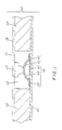
- Fig. 5 shows a switching unit 40 according to the fourth embodiment of the invention which uses the EL device 28 of the first embodiment.
- the switching unit 40 also includes a spacer 49, a protrusion 47, a switch assembly 46, and a lower insulating substrate 41.
- the spacer 49 is formed with a resin film having applied on its both surfaces adhesive and bonds the second insulating layer 27 of the EL device 28 and the lower insulating substrate 41 together.
- the spacer 49 has an opening 48 within which the switching assembly 46 is disposed.
- the protrusion 47 is formed on the lower surface of the second insulating layer 27 of the EL device 28 using epoxy resin and functions as a push button.
- the switching assembly 46 includes a stationary contact 42, a diaphragm moving contact 44, and a stationary contact 43.
- the stationary contact 42 is made of a conductive paper-base phenolic resin and formed on the lower insulating substrate 41 in a C-shape.
- the stationary contact 43 is made of a conductive disc member and disposed inside the stationary contact 42 on the lower insulating substrate 41.
- the diaphragm moving contact 44 is formed with a dome-shaped metallic spring made of phosphor bronze or stainless steel and projects upwards, as viewed in the drawing, in constant engagement with the protrusion 47 with both ends being attached to the stationary contact 42 using an adhesive tape 45.
- the structure of this embodiment gives an operator a moderate switching reaction against depression of the protrusion 47.
- Fig. 6 shows a switching unit according to the fifth embodiment of the invention which is a modification of the one shown in Fig. 4.
- the switching unit of this embodiment includes a diaphragm spring 50 and a spacer 51.
- the diaphragm spring 50 leads from a flat plate 52 and is made by thermally drawing a 100 ⁇ m-thick transparent resin film into a dome-shape.
- the spacer 51 is made of a 100 ⁇ m-thick transparent resin film and has an opening 61.
- the spacer 51 has applied on its both surfaces adhesive and bonds the flat surface 52 and the EL device 20 together so that the top of the diaphragm spring 50 is aligned with the moving and stationary contacts 39 and 35.
- the structure of this embodiment has disposed on the EL device 28 the spacer 51 and the diaphragm spring 50, however, these are made of transparent films, respectively, and do not disturb illumination of the EL device 28.
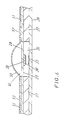
- Fig. 7 shows a switch unit according to the sixth embodiment of the invention which is a modification of the one shown in Fig. 4 different only in structure of the EL device 28.
- the EL device 28 is, as clearly shown in the drawing, thermally pressed to form a recessed portion 53 projecting inward.
- the moving contact 54 is printed using a silver or carbon resin conductive paste on a flat bottom surface of the recessed portion 53 facing the stationary contact 35.
- the structure of this embodiment compensates for some degree of locational error in manual depression in a switching operation.
- Fig. 8 shows an EL device 55 according to the seventh embodiment which is different from the one shown in Fig. 1 only in that the first insulating layer 24 is disposed at the bottom of the EL device 55 instead of the second insulating layer 27.
- the second dielectric layer 25 is printed on the lower surface of the first back electrode layer 23.
- the second back electrode layer 26 is printed on the lower surface of the second dielectric layer 25.
- the first insulating layer 24 is printed on the lower surface of the second back electrode layer 26.
- the EL device 55 has a thickness of approximately 0.3mm.
- the EL device 55 is, as apparent from the above, smaller in number of insulating layers than the EL device 28 of the first embodiment by one, thus resulting in a decrease in production cost.
- the EL device 55 may be used in any of the switch units of the above embodiments.
- Fig. 9 shows an EL device 57 according to the ninth embodiment of the invention which is different from the one shown in Fig. 1 only in that a transparent insulating layer 56 is disposed between the transparent electrode layer 20 and the electroluminescent layer 21.
- the transparent insulating layer 56 is made of a binder resin paste over which a barium titanate powder is stirred and distributed.
- the transparent insulating layer 56 may alternatively be disposed between the electroluminescent layer 21 and the first dielectric layer 22 or between the first dielectric layer 22 and the first back electrode layer 23.
- the EL device 57 has a thickness of approximately 0.3mm and may be used in any of the switch units of the above embodiments. These arrangements may be used with the EL device as shown in Fig. 8.
- the structure of this embodiment provides a high-withstand voltage that can be applied across the transparent electrode layer 20 and the first back electrode layer 23.
- the dispersion electroluminescent device includes three electrodes: first and second electrode layers and a common electrode layer.
- the common electrode layer is disposed between the first and second electrode layers.
- An electroluminescent layer and a first dielectric layer are disposed between the first electrode layer and the common electrode layer.
- a second dielectric layer is disposed between the common electrode layer and the second electrode layer.
- a voltage source applies first and second ac or dc pulse voltages, which are 180° out of phase with each other, across the first electrode layer and the common electrode layer and across the common electrode layer and the second electrode layer, respectively, for canceling mechanical vibrations produced at the first and second dielectric layers by each other.
Landscapes
- Electroluminescent Light Sources (AREA)
- Push-Button Switches (AREA)
- Switch Cases, Indication, And Locking (AREA)
Claims (11)
- Elektrolumineszenzvorrichtung mit:dadurch gekennzeichnet, daßeinem elastischen, transparenten, isolierenden Substrat (19);einer an dem elastischen, transparenten, isolierenden Substrat (19) ausgebildeten, transparenten Elektrodenschicht (20);einer Elektrolumineszenzschicht (21);einer an der Elektrolumineszenzschicht (21) ausgebildeten, ersten dielektrischen Schicht (22);einer an der ersten dielektrischen Schicht (22) ausgebildeten ersten hinteren Elektrodenschicht (23);einer an der ersten hinteren Elektrode (23) ausgebildeten zweiten dielektrischen Schicht (25) undeiner Spannungsquellenschaltung (29), die eine erste Spannung mit einer bestimmten Frequenz und eine zweite Spannung mit der bestimmten Frequenz an die Elektrolumineszenzvorrichtung anlegt, wobei die erste Spannung bezüglich der zweiten Spannung eine Phasenverschiebung von 180° aufweist,
die Elektrolumineszenzschicht (21) an der transparenten Elektrodenschicht (20) ausgebildet ist;
eine zweite hintere Elektrodenschicht (26) an der zweiten dielektrischen Schicht (25) ausgebildet ist;
eine isolierende Schicht (24) an der zweiten hinteren Elektrodenschicht ausgebildet ist und
die erste und zweite dielektrische Schicht (22, 25) piezoelektrische Eigenschaften aufweisen;
wobei die erste Spannung zwischen der ersten hinteren Elektrodenschicht (23) und der transparenten Elektrodenschicht (20) angelegt ist und die zweite Spannung zwischen der ersten hinteren Elektrodenschicht (23) und der zweiten hinteren Elektrodenschicht (26) angelegt ist. - Elektrolumineszenzvorrichtung nach Anspruch 1, ferner mit einer zwischen der ersten hinteren Elektrodenschicht (23) und der zweiten dielektrischen Schicht (25) ausgebildeten weiteren isolierenden Schicht (24).
- Elektrolumineszenzvorrichtung nach Anspruch 1 oder 2, ferner mit einer isolierende Schicht (56), die an einer ersten Stelle zwischen der transparenten Elektrodenschicht (20) und der Elektrolumineszenzschicht (21), an einer zweiten Stelle zwischen der Elektrolumineszenzschicht (21) und der ersten dielektrischen Schicht (22) oder an einer dritten Stelle zwischen der ersten dielektrischen Schicht (22) und der ersten hinteren Elektrodenschicht (23) angeordnet ist.
- Elektrolumineszenzvorrichtung nach einem der Ansprüche 1 bis 3, wobei die erste und die zweite Spannung einer Wechselspannung entsprechen.
- Elektrolumineszenzvorrichtung nach einem der Ansprüche 1 bis 3, wobei die erste und die zweite Spannung einer gepulsten Gleichspannung entsprechen.
- Schalteinheit mit
einer Elektrolumineszenzvorrichtung (28; 55; 57) nach einem der Ansprüche 1 bis 5;
einem isolierenden Substrat (34);
einem an dem isolierenden Substrat (34) angeordneten feststehenden Kontakt (35);
einem beweglichen Kontakt (33), der mit einem bestimmten Abstand vom feststehenden Kontakt (39) entfernt an der Unterseite der isolierenden Schicht (24; 27) gegenüber der Oberseite angeordnet ist, an welcher die zweite hintere Elektrodenschicht (26) ausgebildet ist, und
einem zwischen der isolierenden Schicht (24; 27) der Elektrolumineszenzvorrichtung (28; 55; 57) und dem isolierenden Substrat (34) angeordneten Abstandhalter (37), wobei der Abstandhalter (37) eine Öffnung zur Exposition des beweglichen Kontakts (33) hinsichtlich des feststehenden Kontakts aufweist. - Schalteinheit nach Anspruch 6, ferner mit einem von der Unterseite der isolierenden Schicht (24; 27) zu dem isolierenden Substrat (34) hin verlaufenden Vorsprung (38), wobei der bewegliche Kontakt (39) an dem Vorsprung(38), angeordnet ist so daß dieser dem feststehenden Kontakt (35) gegenüberliegt.
- Schalteinheit nach Anspruch 7, wobei der Vorsprung(38) mit einem isolierenden Harz ausgebildet ist, das an der Unterseite der isolierenden Schicht (24; 27) gedruckt ist.
- Schalteinheit nach Anspruch 7, wobei der Vorsprung mit einem zu dem isolierenden Substrat hin vertieften Abschnitt(53) der Elektrolumineszenzvorrichtung (28) ausgebildet ist.
- Schalteinheit nach Anspruch 6, ferner mit einer aus einem transparenten Harz hergestellten Membranfeder (50), die über dem elastischen, transparenten, isolierenden Substrat (19) der Elektrolumineszenzvorrichtung (28) angeordnet ist, wobei die Membranfeder (50) nach außen gekrümmt ist, so daß sie sich bei Betätigung zur Ausbildung eines Kontaktes zwischen dem feststehenden (35) und dem beweglichen Kontakt (39) verformt.
- Schalteinheit mit:wobei der bewegliche Kontakt (44) mit dem ersten feststehenden Kontakt (42) verbunden ist und sich über den zweiten feststehenden Kontakt (43) erstreckt undeiner Elektrolumineszenzvorrichtung (28; 55; 57) gemäß einem der Ansprüche 1 bis 5;einem isolierenden Substrat (41);einem zwischen der isolierenden Schicht (24; 27) und dem isolierenden Substrat (41) angeordneten Abstandhalter (49), wobei der Abstandhalter (49) eine zwischen der isolierenden Schicht (24; 27) und dem isolierenden Substrat (41) festgelegte Öffnung (48) aufweist;einem ersten feststehenden Kontakt (42), der an dem isolierenden Substrat (41) in der Öffnung (48) des Abstandhalters (49) angeordnet ist;einem in der Öffnung (48) des Abstandhalters (49) an dem isolierenden Substrat (41) mit einem bestimmten Abstand vom ersten feststehenden Kontakt (42) entfernt angeordneten zweiten feststehenden Kontakt (43);einem aus einer flexiblen, gekrümmten, metallischen Platte hergestellten beweglichen Kontakt (44), der in der Öffnung (48) des Abstandhalters (49) angeordnet ist,
einem an der isolierenden Schicht (24; 27) der Elektrolumineszenzvorrrichtung (28; 55; 57) ausgebildeten Vorsprungselement (47), das sich im Eingriff mit einem Abschnitt des beweglichen Kontakts (44) in einer Ausrichtung bezüglich des zweiten feststehenden Kontakts (43) befindet, so daß eine Betätigung des Vorsprungs (47) über die Elektrolumineszenzvorrrichtung (28; 55; 57) zu einem Kontakt zwischen dem ersten und dem zweiten feststehenden Kontakt (42, 43) führt.
Applications Claiming Priority (3)
| Application Number | Priority Date | Filing Date | Title |
|---|---|---|---|
| JP8044526A JPH09245969A (ja) | 1996-03-01 | 1996-03-01 | 分散型エレクトロ・ルミネセンス素子およびそれを用いた照光式スイッチユニット |
| JP44526/96 | 1996-03-01 | ||
| JP4452696 | 1996-03-01 |
Publications (3)
| Publication Number | Publication Date |
|---|---|
| EP0793247A2 EP0793247A2 (de) | 1997-09-03 |
| EP0793247A3 EP0793247A3 (de) | 1998-09-16 |
| EP0793247B1 true EP0793247B1 (de) | 2002-05-22 |
Family
ID=12693972
Family Applications (1)
| Application Number | Title | Priority Date | Filing Date |
|---|---|---|---|
| EP97103288A Expired - Lifetime EP0793247B1 (de) | 1996-03-01 | 1997-02-27 | Geräuscharme Dispersionselektrolumineszenzvorrichtung, und Schalter der diese verwendet |
Country Status (5)
| Country | Link |
|---|---|
| US (1) | US5818174A (de) |
| EP (1) | EP0793247B1 (de) |
| JP (1) | JPH09245969A (de) |
| DE (1) | DE69712661T2 (de) |
| TW (1) | TW352441B (de) |
Families Citing this family (17)
| Publication number | Priority date | Publication date | Assignee | Title |
|---|---|---|---|---|
| US5797482A (en) * | 1996-11-25 | 1998-08-25 | Metro-Mark, Inc. | Electroluminescent keypad |
| AT405633B (de) * | 1997-10-13 | 1999-10-25 | Magna Auteca Zweigniederlassun | Leuchtvorrichtung |
| JP2000003633A (ja) * | 1998-06-16 | 2000-01-07 | Alps Electric Co Ltd | メンブレンスイッチ |
| JP2000010570A (ja) * | 1998-06-24 | 2000-01-14 | Nec Saitama Ltd | El素子の雑音低減を図った小型携帯機器 |
| US20010037933A1 (en) * | 1999-06-17 | 2001-11-08 | Hunter Richard Stuart | Illuminated membrane switch |
| US6046417A (en) * | 1999-01-08 | 2000-04-04 | M.P. Menze Research & Development, Inc. | Membrane supported and actuated switching mechanism |
| US6677709B1 (en) * | 2000-07-18 | 2004-01-13 | General Electric Company | Micro electromechanical system controlled organic led and pixel arrays and method of using and of manufacturing same |
| US6396218B1 (en) * | 2000-10-03 | 2002-05-28 | Xerox Corporation | Multisegment electroluminescent source for a scanner |
| JP2002299067A (ja) * | 2001-04-03 | 2002-10-11 | Matsushita Electric Ind Co Ltd | El素子及びこれを用いた照光装置 |
| DE20212471U1 (de) | 2002-08-13 | 2003-02-06 | FER Fahrzeugelektrik GmbH, 99817 Eisenach | Beleuchtungsvorrichtung |
| US20050077535A1 (en) * | 2003-10-08 | 2005-04-14 | Joinscan Electronics Co., Ltd | LED and its manufacturing process |
| GB0403854D0 (en) * | 2004-02-20 | 2004-03-24 | Pelikon Ltd | Switches |
| US7173204B2 (en) * | 2004-05-14 | 2007-02-06 | Lear Corporation | Control panel assembly with moveable illuminating button and method of making the same |
| US7049536B1 (en) | 2005-06-09 | 2006-05-23 | Oryon Technologies, Llc | Electroluminescent lamp membrane switch |
| US8110765B2 (en) * | 2005-06-09 | 2012-02-07 | Oryon Technologies, Llc | Electroluminescent lamp membrane switch |
| US7445350B2 (en) * | 2005-08-22 | 2008-11-04 | Nissan Technical Center North America, Inc. | Interior/exterior component with electroluminescent lighting and soft touch switching |
| CN100568578C (zh) * | 2006-07-18 | 2009-12-09 | 东莞莫仕连接器有限公司 | 电致发光灯以及其与金属按键板的组合以及其制造方法 |
Family Cites Families (14)
| Publication number | Priority date | Publication date | Assignee | Title |
|---|---|---|---|---|
| US3760137A (en) * | 1970-10-05 | 1973-09-18 | Alps Electric Co Ltd | Matrix push-button switch |
| US4532395A (en) * | 1983-09-20 | 1985-07-30 | Timex Corporation | Electroluminescent flexible touch switch panel |
| JPS60247693A (ja) * | 1984-05-23 | 1985-12-07 | シャープ株式会社 | 薄膜el表示装置の駆動方法 |
| DE3562436D1 (en) * | 1984-05-31 | 1988-06-01 | Philips Nv | Thin film electroluminescent device |
| DE3511496A1 (de) * | 1985-03-29 | 1986-10-09 | Telefunken electronic GmbH, 7100 Heilbronn | Tastschalteinrichtung mit einer durchsichtigen abdeckfolie |
| JPH0634151B2 (ja) * | 1985-06-10 | 1994-05-02 | シャープ株式会社 | 薄膜el表示装置の駆動回路 |
| JPS63307691A (ja) * | 1987-06-09 | 1988-12-15 | Nec Corp | セラミック絶縁薄膜el素子 |
| CH676063A5 (de) * | 1988-02-01 | 1990-11-30 | Fela E Uhlmann Ag Fuer Gedruck | |
| US5325107A (en) * | 1988-11-30 | 1994-06-28 | Sharp Kabushiki Kaisha | Method and apparatus for driving a display device |
| JP2775941B2 (ja) * | 1989-12-08 | 1998-07-16 | 株式会社日本自動車部品総合研究所 | El素子の駆動装置 |
| DE4116006A1 (de) * | 1991-05-16 | 1992-11-19 | Telefonbau & Normalzeit Gmbh | Tastatur fuer elektrotechnische geraete, insbesondere kommunikations-endgeraete |
| US5416494A (en) * | 1991-12-24 | 1995-05-16 | Nippondenso Co., Ltd. | Electroluminescent display |
| JPH08505000A (ja) * | 1992-12-16 | 1996-05-28 | デュレル・コーポレイション | 電界発光ランプ装置とその製造 |
| US5552679A (en) * | 1993-07-15 | 1996-09-03 | International En-R-Tech Incorporated | Electroluminescent and light reflective panel |
-
1996
- 1996-03-01 JP JP8044526A patent/JPH09245969A/ja active Pending
-
1997
- 1997-02-27 TW TW086102436A patent/TW352441B/zh not_active IP Right Cessation
- 1997-02-27 DE DE69712661T patent/DE69712661T2/de not_active Expired - Lifetime
- 1997-02-27 EP EP97103288A patent/EP0793247B1/de not_active Expired - Lifetime
- 1997-02-28 US US08/808,645 patent/US5818174A/en not_active Expired - Lifetime
Also Published As
| Publication number | Publication date |
|---|---|
| US5818174A (en) | 1998-10-06 |
| DE69712661D1 (de) | 2002-06-27 |
| JPH09245969A (ja) | 1997-09-19 |
| DE69712661T2 (de) | 2002-10-24 |
| EP0793247A3 (de) | 1998-09-16 |
| TW352441B (en) | 1999-02-11 |
| EP0793247A2 (de) | 1997-09-03 |
Similar Documents
| Publication | Publication Date | Title |
|---|---|---|
| US5818174A (en) | Noiseless dispersion electroluminescent device and switch unit using same | |
| US7027036B2 (en) | Keypad for mobile phone | |
| US6373008B1 (en) | Light illuminating type switch | |
| KR200358531Y1 (ko) | El 메탈 돔 키패드 | |
| US7991147B2 (en) | Handset device with laminated architecture | |
| US7834853B2 (en) | Handset keypad | |
| US7620175B2 (en) | Handset device with audio porting | |
| US9672998B2 (en) | Push switch | |
| US20080019502A1 (en) | User interface substrate for handset device having an audio port | |
| JPH0935571A (ja) | 照光式スイッチユニット | |
| WO2007094484A1 (ja) | 照光式スイッチおよびこれを有する電子機器 | |
| JPH11232956A (ja) | El付きシートスイッチ | |
| WO2008017191A1 (en) | Sub-assembly for handset device | |
| JP3212621B2 (ja) | エレクトロルミネッセンスライト及びそのシールド構造 | |
| KR101266679B1 (ko) | 전자 기기 및 프린트 기판 모듈 | |
| KR100838544B1 (ko) | 판 스프링이 부착된 시트, 및 이 판 스프링이 부착된시트를 사용한 스위치 장치 | |
| JPH1139984A (ja) | El照光式スイッチ | |
| EP1329920A1 (de) | Schaltereinheit und Verfahren zur elektrischen Verbindung eines elektromagnetischen Abschirmelementes mit einer Erdungsklemme in einer Schaltereinheit | |
| EP1006543A1 (de) | Beleuchtete Membrane für einen elektrischen Schalter | |
| JPH10106754A (ja) | 分散型エレクトロルミネセンス素子配線板およびそれを用いた照光式スイッチユニット | |
| JPH0982168A (ja) | 照光式スイッチユニット | |
| JP2001028220A (ja) | 携帯電話用操作スイッチ | |
| JP2000268656A (ja) | 照光式スイッチ | |
| HK1056644B (en) | Switch unit, and method of electrically connecting an electromagnetic wave shielding member with a grounding terminal in a switch unit |
Legal Events
| Date | Code | Title | Description |
|---|---|---|---|
| PUAI | Public reference made under article 153(3) epc to a published international application that has entered the european phase |
Free format text: ORIGINAL CODE: 0009012 |
|
| 17P | Request for examination filed |
Effective date: 19970227 |
|
| AK | Designated contracting states |
Kind code of ref document: A2 Designated state(s): DE FR GB |
|
| PUAL | Search report despatched |
Free format text: ORIGINAL CODE: 0009013 |
|
| AK | Designated contracting states |
Kind code of ref document: A3 Designated state(s): DE FR GB |
|
| 17Q | First examination report despatched |
Effective date: 20001201 |
|
| GRAG | Despatch of communication of intention to grant |
Free format text: ORIGINAL CODE: EPIDOS AGRA |
|
| GRAG | Despatch of communication of intention to grant |
Free format text: ORIGINAL CODE: EPIDOS AGRA |
|
| GRAH | Despatch of communication of intention to grant a patent |
Free format text: ORIGINAL CODE: EPIDOS IGRA |
|
| GRAH | Despatch of communication of intention to grant a patent |
Free format text: ORIGINAL CODE: EPIDOS IGRA |
|
| GRAA | (expected) grant |
Free format text: ORIGINAL CODE: 0009210 |
|
| REG | Reference to a national code |
Ref country code: GB Ref legal event code: FG4D |
|
| REF | Corresponds to: |
Ref document number: 69712661 Country of ref document: DE Date of ref document: 20020627 |
|
| ET | Fr: translation filed | ||
| PLBE | No opposition filed within time limit |
Free format text: ORIGINAL CODE: 0009261 |
|
| STAA | Information on the status of an ep patent application or granted ep patent |
Free format text: STATUS: NO OPPOSITION FILED WITHIN TIME LIMIT |
|
| 26N | No opposition filed |
Effective date: 20030225 |
|
| PGFP | Annual fee paid to national office [announced via postgrant information from national office to epo] |
Ref country code: FR Payment date: 20120221 Year of fee payment: 16 |
|
| PGFP | Annual fee paid to national office [announced via postgrant information from national office to epo] |
Ref country code: DE Payment date: 20120222 Year of fee payment: 16 |
|
| PGFP | Annual fee paid to national office [announced via postgrant information from national office to epo] |
Ref country code: GB Payment date: 20120222 Year of fee payment: 16 |
|
| GBPC | Gb: european patent ceased through non-payment of renewal fee |
Effective date: 20130227 |
|
| REG | Reference to a national code |
Ref country code: FR Ref legal event code: ST Effective date: 20131031 |
|
| REG | Reference to a national code |
Ref country code: DE Ref legal event code: R119 Ref document number: 69712661 Country of ref document: DE Effective date: 20130903 |
|
| PG25 | Lapsed in a contracting state [announced via postgrant information from national office to epo] |
Ref country code: DE Free format text: LAPSE BECAUSE OF NON-PAYMENT OF DUE FEES Effective date: 20130903 Ref country code: FR Free format text: LAPSE BECAUSE OF NON-PAYMENT OF DUE FEES Effective date: 20130228 Ref country code: GB Free format text: LAPSE BECAUSE OF NON-PAYMENT OF DUE FEES Effective date: 20130227 |