EP0801416A1 - Chambre de traitement à plasma avec assemblage epicyclique d'aimants - Google Patents
Chambre de traitement à plasma avec assemblage epicyclique d'aimants Download PDFInfo
- Publication number
- EP0801416A1 EP0801416A1 EP97302164A EP97302164A EP0801416A1 EP 0801416 A1 EP0801416 A1 EP 0801416A1 EP 97302164 A EP97302164 A EP 97302164A EP 97302164 A EP97302164 A EP 97302164A EP 0801416 A1 EP0801416 A1 EP 0801416A1
- Authority
- EP
- European Patent Office
- Prior art keywords
- axis
- shaft
- gear
- magnetron source
- magnet assembly
- Prior art date
- Legal status (The legal status is an assumption and is not a legal conclusion. Google has not performed a legal analysis and makes no representation as to the accuracy of the status listed.)
- Withdrawn
Links
Images


Classifications
-
- C—CHEMISTRY; METALLURGY
- C23—COATING METALLIC MATERIAL; COATING MATERIAL WITH METALLIC MATERIAL; CHEMICAL SURFACE TREATMENT; DIFFUSION TREATMENT OF METALLIC MATERIAL; COATING BY VACUUM EVAPORATION, BY SPUTTERING, BY ION IMPLANTATION OR BY CHEMICAL VAPOUR DEPOSITION, IN GENERAL; INHIBITING CORROSION OF METALLIC MATERIAL OR INCRUSTATION IN GENERAL
- C23C—COATING METALLIC MATERIAL; COATING MATERIAL WITH METALLIC MATERIAL; SURFACE TREATMENT OF METALLIC MATERIAL BY DIFFUSION INTO THE SURFACE, BY CHEMICAL CONVERSION OR SUBSTITUTION; COATING BY VACUUM EVAPORATION, BY SPUTTERING, BY ION IMPLANTATION OR BY CHEMICAL VAPOUR DEPOSITION, IN GENERAL
- C23C14/00—Coating by vacuum evaporation, by sputtering or by ion implantation of the coating forming material
- C23C14/22—Coating by vacuum evaporation, by sputtering or by ion implantation of the coating forming material characterised by the process of coating
- C23C14/34—Sputtering
- C23C14/35—Sputtering by application of a magnetic field, e.g. magnetron sputtering
-
- H—ELECTRICITY
- H01—ELECTRIC ELEMENTS
- H01J—ELECTRIC DISCHARGE TUBES OR DISCHARGE LAMPS
- H01J37/00—Discharge tubes with provision for introducing objects or material to be exposed to the discharge, e.g. for the purpose of examination or processing thereof
- H01J37/32—Gas-filled discharge tubes
- H01J37/34—Gas-filled discharge tubes operating with cathodic sputtering
- H01J37/3411—Constructional aspects of the reactor
- H01J37/345—Magnet arrangements in particular for cathodic sputtering apparatus
- H01J37/3455—Movable magnets
-
- H—ELECTRICITY
- H01—ELECTRIC ELEMENTS
- H01J—ELECTRIC DISCHARGE TUBES OR DISCHARGE LAMPS
- H01J37/00—Discharge tubes with provision for introducing objects or material to be exposed to the discharge, e.g. for the purpose of examination or processing thereof
- H01J37/32—Gas-filled discharge tubes
- H01J37/34—Gas-filled discharge tubes operating with cathodic sputtering
- H01J37/3402—Gas-filled discharge tubes operating with cathodic sputtering using supplementary magnetic fields
- H01J37/3405—Magnetron sputtering
- H01J37/3408—Planar magnetron sputtering
-
- C—CHEMISTRY; METALLURGY
- C23—COATING METALLIC MATERIAL; COATING MATERIAL WITH METALLIC MATERIAL; CHEMICAL SURFACE TREATMENT; DIFFUSION TREATMENT OF METALLIC MATERIAL; COATING BY VACUUM EVAPORATION, BY SPUTTERING, BY ION IMPLANTATION OR BY CHEMICAL VAPOUR DEPOSITION, IN GENERAL; INHIBITING CORROSION OF METALLIC MATERIAL OR INCRUSTATION IN GENERAL
- C23C—COATING METALLIC MATERIAL; COATING MATERIAL WITH METALLIC MATERIAL; SURFACE TREATMENT OF METALLIC MATERIAL BY DIFFUSION INTO THE SURFACE, BY CHEMICAL CONVERSION OR SUBSTITUTION; COATING BY VACUUM EVAPORATION, BY SPUTTERING, BY ION IMPLANTATION OR BY CHEMICAL VAPOUR DEPOSITION, IN GENERAL
- C23C14/00—Coating by vacuum evaporation, by sputtering or by ion implantation of the coating forming material
- C23C14/22—Coating by vacuum evaporation, by sputtering or by ion implantation of the coating forming material characterised by the process of coating
- C23C14/34—Sputtering
- C23C14/3407—Cathode assembly for sputtering apparatus, e.g. Target
Definitions
- the invention relates generally to sputtering deposition systems and to a planar magnetron source in a plasma processing chamber, such as is used to process semiconductor wafers and other substrates.
- a target In general in a sputtering deposition system, high energy particles bombard a target so as to eject material from the target onto a vorkpiece, e.g. a semiconductor wafer.
- the bombarding particles are generally ions of a heavy inert gas such as argon which are accelerated to high velocities in directions that are substantially perpendicular to the face of the target.
- Plasma sputter deposition systems typically include a platform within a vacuum chamber that supports the wafer next to the face of the target. A voltage supply biases the target negatively relative to the wafer and this bias voltage produces an electric field across a plasma sheath that is formed next to the target.
- the electric field across the plasma sheath is substantially perpendicular to the face of the target.
- the ion densities which are created within the plasma sheath determine the rate of sputtering that is achievable.
- the ion densities at the target are further enhanced by producing within the plasma sheath next to the target a magnetic field that helps trap electrons near the target so that they may be directed into the target by the electric field.
- the magnetic field at the face of the target is usually generated by magnets that are placed behind the target.
- magnetron assemblies have been designed that sputter or erode the target in a particular manner.
- Two such designs are described in greater detail in U.S. 5,320,728, entitled “Planar Magnetron Sputtering Source Producing Improved Coating Thickness Uniformity, Step Coverage and Step Coverage Uniformity", issued June 14, 1994; and in U.S. 5,242,566, entitled “Planar Magnetron Sputtering Source Enabling a Controlled Sputtering Profile Out to the Target Perimeter,” issued September 7, 1993, both of which are assigned to the assignee of the present invention and both of which are incorporated herein by reference.
- the magnet assemblies within those described magnetron sources are rotated to produce the desired erosion patterns that produce higher quality deposited layers on the wafers.
- such magnetron sources cause the target to erode in a manner which produces multiple grooves in the target.
- the nonuniform target erosion produces superior deposited layers, it has associated with it at least two significant disadvantages, namely, shorter target life and wasted target material.
- the target must be replaced before the erosion grooves penetrate the target and the backing plate becomes exposed to the sputtering plasma. Sputtering the backing plate will contaminate the plasma process and destroy product.
- target material can be very expensive, this waste can be quite costly. Therefore, it is desirable to design a magnetron source which still yields the advantages of these earlier designs but also produces extended target life as well as more effective use of the target.
- the invention is a magnetron source for use with a target in a sputtering chamber.
- the magnetron source includes a first shaft having a first axis; a second shaft having a second axis that is parallel to and offset from the first axis; a magnet assembly mounted on the second shaft; and a gear assembly which in response to rotation of the first shaft causes the second shaft to rotate and causes the magnet assembly to rotate about the second axis while the second axis rotates around the first axis, so that the magnet assembly sweeps over an area having a maximum dimension relative to the first axis of R max .
- the magnet assembly has a maximum effective radial dimension relative the second axis of r max , and r max > 0.5 R max .
- the gear assembly is characterized by a gear ratio which is such that the second axis rotates around the first axis at a faster rate than the magnet assembly rotates about the second axis.
- the magnetron source also includes a housing which defines an internal cavity containing the magnet assembly, the first and second shafts, and the gear assembly.
- the housing includes an inlet port and an outlet port through which a coolant is circulated through the internal cavity during operation.
- the gear assembly is made up of a ring gear; and an epicyclic gear located inside of and engaging the ring gear, with the second shaft coupled to the epicyclic gear.
- the gear assembly also includes an arm coupled to the first shaft and having a third shaft coupled thereto.
- the third shaft has an axis that is parallel to and offset from the first shaft, and the epicyclic gear is rotatably mounted on the third shaft.
- the first and third shafts are axially aligned with each other.
- the arm includes a counterweight located on a side of the first shaft that is opposite from the third shaft.
- the gear has gear teeth on an inner perimeter and the epicyclic gear has gear teeth on its outer perimeter which engage the gear teeth of the ring gear.
- the housing also includes a backer plate for holding a target and there is a target mounted on the backer plate.
- the magnet assembly includes an inner pole piece, an outer pole piece, and a plurality of magnets each having first and second pole faces, one of which is coupled to the first pole piece and the other of which is coupled to the second pole piece.
- the invention is a magnetron source for use with a target in a sputtering chamber.
- the magnetron source includes a first shaft having a first axis; a second shaft having a second axis that is parallel to and offset from the first axis; a magnet assembly mounted on the second shaft and having a maximum radial dimension relative the second axis of r max ; and a gear assembly which in response to rotation of the first shaft causes the second shaft to rotate and causes the magnet assembly to rotate about the second axis while the second axis rotates around the first axis.
- the offset is less than r max .
- the offset is substantially less than r max .
- the invention is a plasma processing system for sputtering material onto a substrate.
- the system includes a chamber body defining a processing cavity; a pedestal located within the processing cavity which holds the substrate during processing; and a magnetron source.
- the magnetron source is as described above.
- the invention results in more effective use of sputtering targets. This is in part achieved by increasing the width of the erosion grooves that are produced in the target as compared to systems which only rotate the magnet about a fixed central axis.
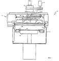
- a sputter deposition system 10 which incorporates the invention includes a vacuum chamber 12 with a planar magnetron source 14, a sputter target 16 which is attached to the magnetron source, and a pedestal 18 for holding a substrate 20 (e.g. semiconductor wafer) onto which material that is sputtered from target 16 is to be deposited.
- Target 16 is made of whatever material is to be deposited onto the substrate. For example, it could be aluminum if an aluminum metalization layer is to be deposited, it could be titanium or titanium nitride if a contact or barrier layer is to be deposited onto the bottoms of contact holes, or it could be tungsten, just to name a few possibilities.
- Magnetron source 14 includes a rotatable magnet assembly 22 which is located behind the target and which is positioned so as to produce a magnetic field that is substantially parallel to the surface of the target at a short distance in front of the target (e.g. 1-3 mm).
- a drive unit 24 e.g. motor
- magnet assembly 22 rotates the magnet assembly in a plane that is parallel to and behind the target.
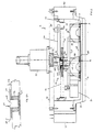
- Magnetron source 14, the design of which is shown in greater detail in Figs. 2 and 3, is constructed so that magnet assembly 22 performs epicyclic motion about a central axis of rotation.
- magnetron source 14 includes a source adapter which encloses the magnet assembly in a cavity through which coolant (e.g. water) is flowed during operation.
- the source adapter includes a housing 50 that is covered on its top end by a top plate 51 and on its bottom side by a backer plate 53 to which the target material is attached, e.g. bonded or fused.
- Inlet and outlet ports 52 and 54 through which coolant is flowed through the inside of source adapter are shown in Fig. 3.
- the magnet assembly is a kidney shaped configuration of multiple magnets 58 that are sandwiched between two pole pieces 60 and 61 on the bottom and a upper circular plate 62 on the top. Magnet assembly 22 is held together by screws which pass through the upper plate, through holes in the individual magnets, and screw into the pole piece to thereby clamp the assembly together.
- an inner pole piece 60 and an outer pole piece 61 there is an inner pole piece 60 and an outer pole piece 61.
- the south poles of the magnets are coupled to inner pole piece 60 and the north poles of the magnets are coupled to outer pole piece 61.
- the bottom surface of the pole pieces are about 1-3 mm from the back surface of backer plate 53. Near the center of the backer plate, the backside as a shallow and gradually sloped indentation (e.g. 1-2 mm deep) so as to improve circulation of coolant through between the pole pieces and the backside of backer plate 53.
- a counterweight 31 is attached to plate 62 so as to counterbalance the magnets.
- magnets are known to persons skilled in the art and thus further details are not be provide here.
- Examples of magnet assemblies that can be used in the present embodiment are described in U.S. 5,320,723 and U.S. 5,242,566 and such magnets are also found on commercially available equipment such as that sold by Applied Materials, Inc. of Santa Clara, CA. (e.g. the Endura 5500 TM or the Cantura TM systems).
- the magnets are Arnaco 5 magnets, which are well known commercially available magnets.
- the movement of the magnet assembly is controlled by a gear arrangement 70 including an outer ring gear 72 and an inner gear 74 (referred to herein as an epicyclic gear 74) which is mounted inside of ring gear 72.
- Ring gear 72 is securely mounted onto source adapter housing 50 and has gear teeth 73 around its inside perimeter.
- Epicyclic gear 74 is a circular gear which has gear teeth 75 around its outer perimeter and which has a diameter that is smaller than the inside diameter of ring gear 72.
- Shaft 30 has a flange 82 at its uppermost end and this flange is screwed into the bottom side of epicyclic gear 74.
- a feedthrough 90 mounted on top of top plate 51 of the magnetron source ashimly includes a bearing-mounted, rotatable shaft 92 which extends into the cavity within source adapter housing 50.
- Feedthrough 90 is driven by a belt 94 (see Fig. 1) that is connected between feedthrough 90 and the output shaft of drive motor 24.
- the feedthrough contains internal seals (not shown), which enable the rotation to be transmitted into the source adapter housing while still maintaining a seal between the inside of source adapter housing and the outside so that coolant within the source adapter housing does not leak out.
- a counterweighted arm 100 is mounted onto drive shaft 92 by means of a clamp 102 that is attached to the top side of arm 100.
- arm 100 rotates with drive shaft 92.
- a spindle 108 that is attached to the bottom side of arm 100 has an axis 110 that is parallel to but offset from the axis of rotation 112 of drive shaft 92 so that when the drive shaft rotates, the spindle revolves around the axis of the drive shaft.
- a counterweight is integrally formed as part of the arm and extending away from spindle 108 and on the other side of axis 112 from spindle 108. The counterweight counterbalances the weight of the spindle 108 and the rest of the gearing mechanism to which spindle 108 is coupled.
- top plate 51 On the top side of counterweighted arm 100 and near the perimeter of the counterweight portion, there is a sensor magnet 57.
- a detector (not shown) above top plate 51 senses the magnetic field that is produced by this sensor magnet and this provides an indication of both the rotation of the gearing mechanism and the rate of that rotation.
- Epicyclic gear 74 is mounted onto spindle 108 by means of a bearing assembly 114 (which is shown in greater detail in Fig. 2A).
- Bearing assembly 114 includes an upper thrust plate 120, a bushing 122, and a lower retainer ring 124 which is screwed into the bottom of spindle 108.
- Retainer ring 124 has a diameter that is larger than the outside diameter of bushing 122.
- Epicyclic gear 74 has a hole located at its center which accommodates bearing assembly 114. An upper portion of the hole has a diameter that is slightly larger than the outer diameter of the bushing; and a lower portion of the hole has a diameter that is larger that the outside diameter of the retainer ring.
- bushing 122 fits within the upper portion of the hole and retainer ring 124 fits within the lower portion of the hole.
- retainer ring 124 is screwed into the bottom of spindle 108, it holds the epicyclic gear onto the spindle.
- the bearing components are made of a common bushing material such as bronze, brass, or copper.
- the offset between the axes of rotation of drive shaft 92 and spindle 108 is such that the gear teeth of epicyclic gear 74 engage with the inside gear teeth of ring gear 72.
- the axis of spindle 108 (indeed, the entire spindle) rotates in a clockwise direction around the axis of drive shaft 92. This causes epicyclic gear 74 to move around the inside perimeter of ring gear 72 and as it does this, it rotates in a counterclockwise direction.
- the gearing ratio of the ring gear to the epicyclic gear is 5:4.
- epicyclic gear 74 and the attached magnet assembly 22 rotates about the axis of spindle 108 at 20 RPM.
- the gear ratio can, of course, be different from that used in the described embodiment. The choice is in part determined by the process that is being performed in the chamber.
- the motion of the magnet assembly can be visualized in the following way.
- R max i.e., the distance from its axis as defined by spindle 108 to its outermost extent.
- the axis of the magnet assembly rotates around the drive shaft axis magnet assembly in an orbit having a radius that is smaller (e.g. much smaller) than R max .
- the magnet assembly Itself is rotating in a counterclockwise direction around its axis at a much slower rate (i.e., a rate that is determined by the gearing ratio).
- Fig. 4 shows the paths that are followed by two different points in the magnet assembly: one point "A” located on the outer edge of the magnet assembly and a second point “B" located as the magnets are rotated by drive motor 24 (also see Fig. 2).
- Center point 130 represents axis 112, i.e., the axis of the drive shaft which located at the center of the target.
- circle 132 represents the path followed by axis 110 as the drive shaft rotates.
- the epicyclic motion of the magnet assembly has the effect of "dithering" the magnetic field. That is, it spreads out the width of the region of the target that is affected by the magnetic field produced by any particular point on the magnet. As should be apparent from Fig. 4, this will have the effect of broadening the sputtering grooves that are formed in the target during operation. Thus, more of the target material can be used before the target has to be replaced.
- the offset should be less than (e.g., substantially less than) r max , and the magnet assembly should generally have an r max that is greater than one half the radius of the area that is swept out by the magnet assembly. Usually, the area that is swept out by the magnet assembly will be quite close to the actual area of the target itself.
- the offset is about 0.5 inch and r max is about 5.75 (i.e., 0.5 x 11.5) inches (for a system that processes 8 inch wafers). In this case, r max is actually greater than about 0.9 times the outer reach of the magnet assembly as it moves over the backside of the target.
- the offset is larger than 0.5 r max , then the intense magnetic field produced by the magnet assembly will not pass over the center of the target and target erosion at the center will thus be considerably less than elsewhere.
- the offset is zero and the spindle was attached directly to the drive shaft, that would be equivalent to the way in which the prior art systems are currently operated (i.e., simple rotation of the kidney-shaped magnet assembly).
- a radius or a maximum dimension of the magnet assembly we mean this to be measured in terms of the reach of the magnetic field that it produces and not by the outside physical dimensions of the assembly.
- the maximum effective radial dimension of the magnet assembly relative to a reference location is defined by the outer reach of the outermost magnetic pole pieces.
- the maximum radius in the cross-section that is illustrated is defined by the point labeled "A”. This is true regardless of how much farther the support structure of the magnetic assembly might actually extend beyond that point. In other words, it is a measure of the outer reach of the magnetic field that passes through the pole pieces in the plane of the pole pieces.
- the area swept over by the magnet assembly we mean an area that is substantially equal in shape and size to the area that is swept over by the pole faces of the magnet assembly.
- the gears and the upper counterweight 100 are made of stainless steel.
- the lower counterweight 81 and the upper plate 62 are made of copper, or some other nonmagnetic material. Of course, this is not to suggest that other materials may not be used in other embodiments.
- a grounded metal shield 19 that extends down into the chamber and reaches below a clamping ring 21 which holds the wafer 20 during processing.
- This metal shield 19 protects the chamber walls from sputtered material.
- the deposition system also typically includes other equipment which is not shown but which is well known in the art.
- it includes a vacuum pump, which is used to evacuate the chamber to achieve the vacuum levels that are desired for sputtering, and it includes one or more sources of process gas (e.g. Argon), which are connected to the chamber through corresponding mass flow controllers.
- process gas e.g. Argon
- the mass flow controllers enable the user to precisely control the rate of flow or process gas into the chamber, thereby also controlling the total pressure in the chamber.
- the system might also include a D.C. power supply which is connected between the target and the pedestal and which delivers the power that is necessary to generate a plasma during operation.
- the supply biases target negatively with respect to an electrically floating pedestal and the grounded chamber.
- coils or antennae mounted either inside and/or outside of the chamber for coupling energy from an RF source into the plasma that is generated in the chamber.
- a programmable control unit (not shown) controls the overall operation of the system, including the operation of mass flow controllers, drive motor 24, the power supplies, and the vacuum pump. That is, it is programmed to fully automate the deposition and cleaning processes which are performed in the system.
Landscapes
- Chemical & Material Sciences (AREA)
- Engineering & Computer Science (AREA)
- Physics & Mathematics (AREA)
- Plasma & Fusion (AREA)
- Analytical Chemistry (AREA)
- Materials Engineering (AREA)
- Chemical Kinetics & Catalysis (AREA)
- Mechanical Engineering (AREA)
- Metallurgy (AREA)
- Organic Chemistry (AREA)
- Physical Vapour Deposition (AREA)
- Electrodes Of Semiconductors (AREA)
- Physical Deposition Of Substances That Are Components Of Semiconductor Devices (AREA)
Applications Claiming Priority (2)
| Application Number | Priority Date | Filing Date | Title |
|---|---|---|---|
| US63021996A | 1996-04-10 | 1996-04-10 | |
| US630219 | 1996-04-10 |
Publications (1)
| Publication Number | Publication Date |
|---|---|
| EP0801416A1 true EP0801416A1 (fr) | 1997-10-15 |
Family
ID=24526281
Family Applications (1)
| Application Number | Title | Priority Date | Filing Date |
|---|---|---|---|
| EP97302164A Withdrawn EP0801416A1 (fr) | 1996-04-10 | 1997-03-27 | Chambre de traitement à plasma avec assemblage epicyclique d'aimants |
Country Status (4)
| Country | Link |
|---|---|
| EP (1) | EP0801416A1 (fr) |
| JP (1) | JPH1030180A (fr) |
| KR (1) | KR970072164A (fr) |
| TW (1) | TW333656B (fr) |
Cited By (7)
| Publication number | Priority date | Publication date | Assignee | Title |
|---|---|---|---|---|
| EP1032944A1 (fr) * | 1997-11-19 | 2000-09-06 | SINVACO n.v. | Magnetron plan ameliore a ensemble aimants mobile |
| US6258217B1 (en) | 1999-09-29 | 2001-07-10 | Plasma-Therm, Inc. | Rotating magnet array and sputter source |
| US7807030B2 (en) | 2002-05-21 | 2010-10-05 | Applied Materials, Inc. | Small scanned magentron |
| WO2013088240A1 (fr) | 2011-12-13 | 2013-06-20 | Sony Corporation | Dispositif de mémoire |
| RU2500834C2 (ru) * | 2011-08-29 | 2013-12-10 | Закрытое акционерное общество "Ферри Ватт" | Распылительный узел плоского магнетрона |
| EP3117449A4 (fr) * | 2014-03-14 | 2017-08-23 | Applied Materials, Inc. | Chambre intelligente et constituants de chambre intelligente |
| CN115110051A (zh) * | 2022-07-12 | 2022-09-27 | 江西贵得科技有限公司 | 一种镀膜旋转靶靶芯结构 |
Families Citing this family (2)
| Publication number | Priority date | Publication date | Assignee | Title |
|---|---|---|---|---|
| US6852202B2 (en) | 2002-05-21 | 2005-02-08 | Applied Materials, Inc. | Small epicyclic magnetron with controlled radial sputtering profile |
| KR101505948B1 (ko) * | 2013-12-16 | 2015-03-26 | 피에스케이 주식회사 | 배플 어셈블리 및 이를 가지는 기판 처리 장치 |
Citations (3)
| Publication number | Priority date | Publication date | Assignee | Title |
|---|---|---|---|---|
| US4714536A (en) * | 1985-08-26 | 1987-12-22 | Varian Associates, Inc. | Planar magnetron sputtering device with combined circumferential and radial movement of magnetic fields |
| US5126029A (en) * | 1990-12-27 | 1992-06-30 | Intel Corporation | Apparatus and method for achieving via step coverage symmetry |
| US5320728A (en) * | 1990-03-30 | 1994-06-14 | Applied Materials, Inc. | Planar magnetron sputtering source producing improved coating thickness uniformity, step coverage and step coverage uniformity |
-
1997
- 1997-03-27 EP EP97302164A patent/EP0801416A1/fr not_active Withdrawn
- 1997-04-01 TW TW086104195A patent/TW333656B/zh active
- 1997-04-09 JP JP9091021A patent/JPH1030180A/ja not_active Withdrawn
- 1997-04-10 KR KR1019970013127A patent/KR970072164A/ko not_active Withdrawn
Patent Citations (3)
| Publication number | Priority date | Publication date | Assignee | Title |
|---|---|---|---|---|
| US4714536A (en) * | 1985-08-26 | 1987-12-22 | Varian Associates, Inc. | Planar magnetron sputtering device with combined circumferential and radial movement of magnetic fields |
| US5320728A (en) * | 1990-03-30 | 1994-06-14 | Applied Materials, Inc. | Planar magnetron sputtering source producing improved coating thickness uniformity, step coverage and step coverage uniformity |
| US5126029A (en) * | 1990-12-27 | 1992-06-30 | Intel Corporation | Apparatus and method for achieving via step coverage symmetry |
Cited By (9)
| Publication number | Priority date | Publication date | Assignee | Title |
|---|---|---|---|---|
| EP1032944A1 (fr) * | 1997-11-19 | 2000-09-06 | SINVACO n.v. | Magnetron plan ameliore a ensemble aimants mobile |
| US6258217B1 (en) | 1999-09-29 | 2001-07-10 | Plasma-Therm, Inc. | Rotating magnet array and sputter source |
| US7807030B2 (en) | 2002-05-21 | 2010-10-05 | Applied Materials, Inc. | Small scanned magentron |
| RU2500834C2 (ru) * | 2011-08-29 | 2013-12-10 | Закрытое акционерное общество "Ферри Ватт" | Распылительный узел плоского магнетрона |
| WO2013088240A1 (fr) | 2011-12-13 | 2013-06-20 | Sony Corporation | Dispositif de mémoire |
| EP3117449A4 (fr) * | 2014-03-14 | 2017-08-23 | Applied Materials, Inc. | Chambre intelligente et constituants de chambre intelligente |
| US10153143B2 (en) | 2014-03-14 | 2018-12-11 | Applied Materials, Inc. | Smart chamber and smart chamber components |
| US10930479B2 (en) | 2014-03-14 | 2021-02-23 | Applied Materials, Inc. | Smart chamber and smart chamber components |
| CN115110051A (zh) * | 2022-07-12 | 2022-09-27 | 江西贵得科技有限公司 | 一种镀膜旋转靶靶芯结构 |
Also Published As
| Publication number | Publication date |
|---|---|
| TW333656B (en) | 1998-06-11 |
| KR970072164A (ko) | 1997-11-07 |
| JPH1030180A (ja) | 1998-02-03 |
Similar Documents
| Publication | Publication Date | Title |
|---|---|---|
| KR101110546B1 (ko) | 마그네트론과 스퍼터 타겟 간의 간격 보상 방법 및 장치 | |
| JP4606162B2 (ja) | 小型遊星マグネトロン | |
| US4714536A (en) | Planar magnetron sputtering device with combined circumferential and radial movement of magnetic fields | |
| US8021527B2 (en) | Coaxial shafts for radial positioning of rotating magnetron | |
| KR102161196B1 (ko) | 증가된 수명 및 스퍼터링 균일도를 가지는 스퍼터링 타겟 | |
| US6841050B2 (en) | Small planetary magnetron | |
| US6258217B1 (en) | Rotating magnet array and sputter source | |
| CA2035106A1 (fr) | Appareil permettant de realiser des depots de particules alignees et methode connexe | |
| WO2006038407A2 (fr) | Appareil de formation de films sous vide | |
| EP0801416A1 (fr) | Chambre de traitement à plasma avec assemblage epicyclique d'aimants | |
| EP0439360A2 (fr) | Appareil de pulvérisation rotative permettant d'obtenir une érosion sélective | |
| US20070261957A1 (en) | Magnetron cathode and sputtering device installing it | |
| EP0439361B1 (fr) | Appareillage de pulvérisation comportant un dispositif tournant à aimants ayant une géométrie permettant d'obtenir un profil d'érosion prédéterminé de la cible | |
| EP0213922A2 (fr) | Dispositif de pulvérisation cathodique planaire à mouvement combiné circonférentiel et radial des champs magnétiques | |
| US20050139467A1 (en) | Sputtering device | |
| WO1991005077A1 (fr) | Appareil et methode de depot ionique en phase vapeur | |
| US5919345A (en) | Uniform film thickness deposition of sputtered materials | |
| JP4219566B2 (ja) | スパッタ装置 | |
| US11932932B2 (en) | Sputtering system with a plurality of cathode assemblies | |
| JPH11340165A (ja) | スパッタリング装置及びマグネトロンユニット | |
| JP4702530B2 (ja) | プラネタリー方式のスパッタリング装置 | |
| WO2022244443A1 (fr) | Unité cathode pour dispositif de pulvérisation à magnétron et dispositif de pulvérisation à magnétron | |
| WO2026085294A1 (fr) | Système de pulvérisation cathodique avec source de mouvement d'aimant |
Legal Events
| Date | Code | Title | Description |
|---|---|---|---|
| PUAI | Public reference made under article 153(3) epc to a published international application that has entered the european phase |
Free format text: ORIGINAL CODE: 0009012 |
|
| AK | Designated contracting states |
Kind code of ref document: A1 Designated state(s): BE DE FR GB IE IT |
|
| STAA | Information on the status of an ep patent application or granted ep patent |
Free format text: STATUS: THE APPLICATION IS DEEMED TO BE WITHDRAWN |
|
| 18D | Application deemed to be withdrawn |
Effective date: 19980416 |