EP0806266A2 - Polierverfahren und -vorrichtung zur Verwendung desselben - Google Patents
Polierverfahren und -vorrichtung zur Verwendung desselben Download PDFInfo
- Publication number
- EP0806266A2 EP0806266A2 EP97302916A EP97302916A EP0806266A2 EP 0806266 A2 EP0806266 A2 EP 0806266A2 EP 97302916 A EP97302916 A EP 97302916A EP 97302916 A EP97302916 A EP 97302916A EP 0806266 A2 EP0806266 A2 EP 0806266A2
- Authority
- EP
- European Patent Office
- Prior art keywords
- layer
- polishing
- detecting
- film thickness
- light beam
- Prior art date
- Legal status (The legal status is an assumption and is not a legal conclusion. Google has not performed a legal analysis and makes no representation as to the accuracy of the status listed.)
- Ceased
Links
Images




Classifications
-
- B—PERFORMING OPERATIONS; TRANSPORTING
- B24—GRINDING; POLISHING
- B24B—MACHINES, DEVICES, OR PROCESSES FOR GRINDING OR POLISHING; DRESSING OR CONDITIONING OF ABRADING SURFACES; FEEDING OF GRINDING, POLISHING, OR LAPPING AGENTS
- B24B37/00—Lapping machines or devices; Accessories
- B24B37/005—Control means for lapping machines or devices
- B24B37/013—Devices or means for detecting lapping completion
-
- B—PERFORMING OPERATIONS; TRANSPORTING
- B24—GRINDING; POLISHING
- B24B—MACHINES, DEVICES, OR PROCESSES FOR GRINDING OR POLISHING; DRESSING OR CONDITIONING OF ABRADING SURFACES; FEEDING OF GRINDING, POLISHING, OR LAPPING AGENTS
- B24B49/00—Measuring or gauging equipment for controlling the feed movement of the grinding tool or work; Arrangements of indicating or measuring equipment, e.g. for indicating the start of the grinding operation
- B24B49/02—Measuring or gauging equipment for controlling the feed movement of the grinding tool or work; Arrangements of indicating or measuring equipment, e.g. for indicating the start of the grinding operation according to the instantaneous size and required size of the workpiece acted upon, the measuring or gauging being continuous or intermittent
- B24B49/04—Measuring or gauging equipment for controlling the feed movement of the grinding tool or work; Arrangements of indicating or measuring equipment, e.g. for indicating the start of the grinding operation according to the instantaneous size and required size of the workpiece acted upon, the measuring or gauging being continuous or intermittent involving measurement of the workpiece at the place of grinding during grinding operation
-
- B—PERFORMING OPERATIONS; TRANSPORTING
- B24—GRINDING; POLISHING
- B24B—MACHINES, DEVICES, OR PROCESSES FOR GRINDING OR POLISHING; DRESSING OR CONDITIONING OF ABRADING SURFACES; FEEDING OF GRINDING, POLISHING, OR LAPPING AGENTS
- B24B49/00—Measuring or gauging equipment for controlling the feed movement of the grinding tool or work; Arrangements of indicating or measuring equipment, e.g. for indicating the start of the grinding operation
- B24B49/12—Measuring or gauging equipment for controlling the feed movement of the grinding tool or work; Arrangements of indicating or measuring equipment, e.g. for indicating the start of the grinding operation involving optical means
-
- G—PHYSICS
- G01—MEASURING; TESTING
- G01B—MEASURING LENGTH, THICKNESS OR SIMILAR LINEAR DIMENSIONS; MEASURING ANGLES; MEASURING AREAS; MEASURING IRREGULARITIES OF SURFACES OR CONTOURS
- G01B11/00—Measuring arrangements characterised by the use of optical techniques
- G01B11/02—Measuring arrangements characterised by the use of optical techniques for measuring length, width or thickness
- G01B11/06—Measuring arrangements characterised by the use of optical techniques for measuring length, width or thickness for measuring thickness ; e.g. of sheet material
- G01B11/0616—Measuring arrangements characterised by the use of optical techniques for measuring length, width or thickness for measuring thickness ; e.g. of sheet material of coating
- G01B11/0683—Measuring arrangements characterised by the use of optical techniques for measuring length, width or thickness for measuring thickness ; e.g. of sheet material of coating measurement during deposition or removal of the layer
-
- G—PHYSICS
- G05—CONTROLLING; REGULATING
- G05B—CONTROL OR REGULATING SYSTEMS IN GENERAL; FUNCTIONAL ELEMENTS OF SUCH SYSTEMS; MONITORING OR TESTING ARRANGEMENTS FOR SUCH SYSTEMS OR ELEMENTS
- G05B19/00—Program-control systems
- G05B19/02—Program-control systems electric
- G05B19/18—Numerical control [NC], i.e. automatically operating machines, in particular machine tools, e.g. in a manufacturing environment, so as to execute positioning, movement or co-ordinated operations by means of program data in numerical form
- G05B19/401—Numerical control [NC], i.e. automatically operating machines, in particular machine tools, e.g. in a manufacturing environment, so as to execute positioning, movement or co-ordinated operations by means of program data in numerical form characterised by control arrangements for measuring, e.g. calibration and initialisation, measuring workpiece for machining purposes
-
- H—ELECTRICITY
- H10—SEMICONDUCTOR DEVICES; ELECTRIC SOLID-STATE DEVICES NOT OTHERWISE PROVIDED FOR
- H10P—GENERIC PROCESSES OR APPARATUS FOR THE MANUFACTURE OR TREATMENT OF DEVICES COVERED BY CLASS H10
- H10P74/00—Testing or measuring during manufacture or treatment of wafers, substrates or devices
- H10P74/23—Testing or measuring during manufacture or treatment of wafers, substrates or devices characterised by multiple measurements, corrections, marking or sorting processes
- H10P74/238—Testing or measuring during manufacture or treatment of wafers, substrates or devices characterised by multiple measurements, corrections, marking or sorting processes comprising acting in response to an ongoing measurement without interruption of processing, e.g. endpoint detection or in-situ thickness measurement
-
- G—PHYSICS
- G05—CONTROLLING; REGULATING
- G05B—CONTROL OR REGULATING SYSTEMS IN GENERAL; FUNCTIONAL ELEMENTS OF SUCH SYSTEMS; MONITORING OR TESTING ARRANGEMENTS FOR SUCH SYSTEMS OR ELEMENTS
- G05B2219/00—Program-control systems
- G05B2219/30—Nc systems
- G05B2219/37—Measurements
- G05B2219/37398—Thickness
-
- G—PHYSICS
- G05—CONTROLLING; REGULATING
- G05B—CONTROL OR REGULATING SYSTEMS IN GENERAL; FUNCTIONAL ELEMENTS OF SUCH SYSTEMS; MONITORING OR TESTING ARRANGEMENTS FOR SUCH SYSTEMS OR ELEMENTS
- G05B2219/00—Program-control systems
- G05B2219/30—Nc systems
- G05B2219/37—Measurements
- G05B2219/37576—Post-process, measure worpiece after machining, use results for new or same
-
- G—PHYSICS
- G05—CONTROLLING; REGULATING
- G05B—CONTROL OR REGULATING SYSTEMS IN GENERAL; FUNCTIONAL ELEMENTS OF SUCH SYSTEMS; MONITORING OR TESTING ARRANGEMENTS FOR SUCH SYSTEMS OR ELEMENTS
- G05B2219/00—Program-control systems
- G05B2219/30—Nc systems
- G05B2219/45—Nc applications
- G05B2219/45026—Circuit board, pcb
-
- G—PHYSICS
- G05—CONTROLLING; REGULATING
- G05B—CONTROL OR REGULATING SYSTEMS IN GENERAL; FUNCTIONAL ELEMENTS OF SUCH SYSTEMS; MONITORING OR TESTING ARRANGEMENTS FOR SUCH SYSTEMS OR ELEMENTS
- G05B2219/00—Program-control systems
- G05B2219/30—Nc systems
- G05B2219/45—Nc applications
- G05B2219/45199—Polish
-
- G—PHYSICS
- G05—CONTROLLING; REGULATING
- G05B—CONTROL OR REGULATING SYSTEMS IN GENERAL; FUNCTIONAL ELEMENTS OF SUCH SYSTEMS; MONITORING OR TESTING ARRANGEMENTS FOR SUCH SYSTEMS OR ELEMENTS
- G05B2219/00—Program-control systems
- G05B2219/30—Nc systems
- G05B2219/50—Machine tool, machine tool null till machine tool work handling
- G05B2219/50067—Measure surface for thickness and store map in memory, machine surface
Definitions
- This invention relates to a polishing method for chemically and mechanically polishing and flattening the surface of a substrate such as a wafer on which dielectric layers on the like are laminated in a semiconductor device manufacturing process or the like and a polishing apparatus using the same, and is suitable, for example, in a lithography process for accurately detecting the termination point of the polishing step for an insulating layer (film layer) applied onto a silicon substrate, making the film thickness of the insulating layer fall within a predetermined range and efficiently performing the process of flattening the surface configuration of the insulating layer to thereby obtain a semiconductor device of a high degree of integration.
- a chemical and mechanical polishing method has heretofore been proposed as the flattening technique of removing the uneven portions or the level difference portions of the surface of a substrate such as a wafer on which wiring or dielectric layers are laminated and flattening the surface.
- a termination point detecting method of monitoring the film thickness and the surface configuration distribution of the surface layer of a substrate such as a wafer to be polished on which dielectric or the like is laminated at a time on the spot and grasping the level of the flattening of the whole surface or the localized flattening, and judging the optimum position for the termination of polishing becomes important in chemical and mechanical polishing.
- polishing termination point detecting methods there are, for example, a method of obtaining the amount of polishing from the polishing time, a method of obtaining a variation in polishing resistance from a variation in the electric current of a motor for driving a polishing stool, etc.
- the method of obtaining the amount of polishing from the polishing time makes it necessary to constantly control conditions such as the pressure force to the surface to be polished, the degree of abrasion of a polishing pad, the slurry density in polishing liquid, the temperature of the surface to be polished, etc. and therefore, it is difficult to detect the termination point accurately.
- the method of detecting a variation in polishing resistance from a variation in the electric current of the motor for driving a polishing stool makes it necessary to separate a signal waveform and noise from each other highly accurately and therefore, it is difficult to detect the termination point accurately and the local polishing situation of the surface to be polished cannot be detected.
- the present invention can provide a polishing method suitable for detecting, when flattening the surface of a substrate such as a wafer on which dielectric or the like is laminated by chemical and mechanical polishing, the surface configuration and film thickness distribution of an insulating layer provided on the surface, and using these values to precisely judge the termination point of the polishing step to thereby efficiently flatten the surface in the semiconductor process and manufacture a semiconductor device of a high degree of integration and a polishing apparatus using the same.
- One aspect of the present invention provides a polishing method of polishing the surface of a layer provided on the surface of a substrate, characterized by:
- the polishing controlling step has the step of stopping the polishing when it is determined by the determining step that both of the surface configuration and film thickness distribution of the layer are within an allowable range.
- the polishing controlling step has the step of stopping the polishing when it is determined by the determining step that the surface configuration of the layer is outside an allowable range and the minimum film thickness of the layer is equal to or less than a reference value.
- the measurement by the surface configuration measuring step and the measurement by the film thickness distribution measuring step are simultaneously effected.
- the same portion of the layer is measured at the surface configuration measuring step and the film thickness distribution measuring step.
- One aspect of the present invention provides a polishing apparatus for driving the surface of a layer provided on the surface of a substrate and polishing means relative to each other to thereby polish the layer, characterized by:
- the detecting means has means for detecting the surface information of the layer at a plurality of locations simultaneously.
- the polishing means has a plurality of partial polishing tools for polishing a portion of the surface of the layer.
- the detecting means has means for measuring the surface location information and film thicknesses at a plurality of locations on the layer.
- the detecting means has distance measuring means for detecting the distance from the surface of the layer to a reference surface.
- the detecting means has film thickness measuring means for measuring the film thickness of the layer.
- the polishing apparatus has control means for determining from a signal from the detecting means by a determining portion whether the surface configuration and film thickness distribution of the layer are within a preset allowable range, and controlling whether to continue or stop the polishing of the layer on the basis of a signal from the determining portion.
- Another aspect of the present invention provides a polishing method of driving the surface of a layer provided on the surface of a substrate and polishing means relative to each other to polish the surface of the layer, characterized by the steps of:
- the surface information of the layer is the surface configuration and film thickness distribution of the layer.
- the step of controlling has the determining step of determining whether the surface configuration and film thickness distribution of the layer are within a preset allowable range.
- the step of controlling has the step of obtaining the surface information of the layer from the difference between the intensity of the reflected light beam from each surface based on the first light beam and the intensity of the reflected light beam from each surface based on the second light beam.
- a further aspect of the present invention provides a polishing apparatus for driving the surface of a layer provided on the surface of a substrate and polishing means relative to each other to thereby polish the layer, characterized by:
- the surface information of the layer is the surface configuration and film thickness distribution of the layer.
- the control means has a determining portion for determining whether the surface configuration and film thickness distribution of the layer are within a preset allowable range.
- the applying means has a semiconductor laser of variable coherent distance.
- the control means finds the surface information of the layer from the difference between the intensity of the reflected light beam from each surface based on the first light beam and the intensity of the reflected light beam from each surface based on the second light beam.
- a still further aspect of the present invention provides a polishing method of driving the surface of a layer provided on the surface of a substrate and polishing means having a polishing pad of an area smaller than that of the surface of the layer relative to each other to thereby polish the layer, characterized by:
- the polishing means is movable in a plane parallel to the surface of the layer, and the detecting step has the step of detecting the surface information of the layer by the utilization of position information from position detecting means for detecting the position information of the polishing means in the plane.
- the detecting step has the step of detecting the distance from the surface of the layer to a reference surface and measuring the film thickness of the layer.
- the detecting step has the step of detecting the surface configuration and film thickness distribution of the layer
- the controlling step has the step of determining whether the surface configuration and film thickness distribution of the layer obtained from the detecting step are within a preset allowable range.
- Another aspect of the present invention provides a polishing apparatus for polishing the surface of a layer provided on the surface of a substrate having:
- the polishing means is movable in a plane parallel to the surface of the layer, and has position detecting means for detecting the position information of the polishing means in the plane, and the detecting means utilizes the position information from the position detecting means to find the surface information of the layer.
- the detecting means has distance measuring means for detecting the distance from the surface of the layer to a reference surface and measuring the film thickness of the layer.
- the polishing apparatus has control means for controlling the continuation or stoppage of the polishing of the layer on the basis of a signal from the detecting means.
- the detecting means has means for detecting the surface configuration and film thickness distribution of the layer, and the control means has a determining portion for determining whether the surface configuration and film thickness distribution of the layer obtained from the detecting means are within a preset allowable range.
- Fig. 1 is a schematic view of portions of Embodiment 1 of the present invention.
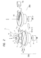
- Fig. 2 is a schematic view of portions of Embodiment 1 of the present invention.
- Figs. 3A and 3B are schematic views of the monitor unit array of Fig. 1.
- Fig. 4 is a schematic view of portions of a sensor according to the present invention.
- Fig. 5 is an enlarged illustration of a portion of Fig. 4.
- Fig. 6 is a flow chart of the operation of Embodiment 1 of the present invention.
- Figs. 7A and 7B are schematic views of portions of Embodiment 2 of the present invention.
- Figs. 8A and 8B are schematic views of portions of Embodiment 3 of the present invention.
- Figs. 9A and 9B are schematic views of portions of Embodiments 4 of the present invention.
- Fig. 10 is a schematic view of portions of Embodiment 5 of the present invention.
- Fig. 11 is a schematic view of portions of Embodiment 6 of the present invention.
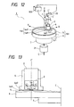
- Fig. 12 is a schematic view of portions of Embodiment 7 of the present invention.
- Fig. 13 is a schematic view of portions of Fig. 12.
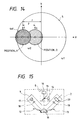
- Fig. 14 is a schematic view of a portion of Fig. 12.
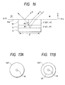
- Fig. 15 is a schematic view of portions of a sensor according to the present invention.
- Fig. 16 is an enlarged illustration of a portion of Fig. 15.
- Figs. 17A and 17B are enlarged illustrations of a portion of Fig. 12.
- Figs. 18A and 18B are illustrations of a measuring method according to Embodiment 7 of the present invention.
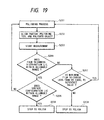
- Fig. 19 is a flow chart of the operation of Embodiment 7 of the present invention.
- Figs. 1 and 2 are schematic views of portions of Embodiment 1 of the present invention.
- the reference numeral 1 designates a chemical and mechanical polishing apparatus.
- Fig. 1 there is shown the manner in which the surface of a polished object 101 is polished, whereafter the supporting portion 101a of the polishing apparatus 1 is moved in X direction and set at the position of a monitor unit array 102 indicated by dotted line.
- Fig. 2 shows a case where the surface information (surface configuration and film thickness distribution) of the workpiece 101 is detected by the fixed monitor unit array (detecting means) 102, and on the basis of the result of the detection by the monitor unit array 102, the termination point or the continuation or stoppage of the polishing step for the workpiece 101 is controlled by control means 103.
- the polished object 101 comprises a structure consisting of an insulating layer (film layer) 5 formed on a silicon substrate 6, and is held on a substrate holder 7.
- the insulating layer 5 on the silicon substrate 6 is partially chemically-mechanically polished by a partial polishing tool 4 which will be described later.
- the substrate holder 7 holds the polished object 101 thereon and is rotated about a rotary shaft C at an angular speed ⁇ 1 by drive means (not shown).
- the rotary shaft C is defined as the Z-axis, and a plane orthogonal thereto is defined as X, Y plane.
- the reference characters 4 (4a, 4b, 4c) denote partial polishing tools.
- the partial polishing tools 4a, 4b, 4c have polishing pads 4a1, 4b1, 4c1 and holders 4a2, 4b2, 4c2 holding the polishing pads 4a1, 4b1, 4c1, and are rotated about rotary shafts C' at an angular speed ⁇ 2 by drive means (not shown).
- Figs. 1 and 2 show a case where the insulating layer 5 on the silicon substrate 6 is partially polished by the three polishing pads 4a1, 4b1, 4c1.
- the polishing openings in the polishing pads 4a1, 4b1, 4c1 are smaller than the polished surface (insulating layer) 5 of the polished object 101. Thereby the insulating layer is partially polished.
- the reference numeral 21 designates an encoder which detects the rotation information of the rotary shaft C.
- the monitor unit array 102 as shown in Figs. 3A and 3B, comprises a plurality of sensors 102a1 - 102an one-dimensionally arranged in the Y-axis direction, and the surface conditions such as the surface configuration and film thickness distribution of the insulating layer 5 on the silicon substrate 6 are inspected by each sensor.
- the partial polishing tool 4 when the surface of the insulating layer 5 is to be polished, the partial polishing tool 4 is rotated about the rotary shafts C' and the substrate holder 7 is rotated about the rotary shaft C, and both of them are driven relative to each other and slurry including a polishing material is caused to flow out from a nozzle (not shown) onto the surface of the polished object 101 while the relative positions of the two in X direction and Y direction are displaced as required, whereby the slurry is uniformly supplied to the interface between the insulating layer 5 and the polishing pads 4a1, 4b1, 4c1.
- the ratio between the pressure and the number of revolutions of the insulating layer 5 and the partial polishing tool 4 and the quantity of slurry supplied are appropriately selected to thereby polish.
- the insulating layer 5 formed on the silicon substrate 6 is partially polished by the partial polishing tool 4 to thereby achieve the flattening of the surface thereof.
- the surface of the insulating layer 5 is partially polished for a preset time, whereafter as shown in Fig. 2, the relative position of the partial polishing tool 4 and the polished object 101 in Z direction is changed to separate the partial polishing tool 4 and the workpiece 101 from each other, and the supporting portion 101a including the substrate holder 7 is moved in X direction and is disposed in opposed relationship with the monitor unit array 102 installed in the Y-axis direction.
- the film thicknesses and surface configuration of the insulating layer 5 on the silicon substrate 6 at a plurality of locations are measured by the monitor unit array 102 while the polished object 101 is being rotated.
- the film thickness information over a wide area of the insulating layer 5 is detected efficiently. Also, with the rotation of the polished object 101, the polished object 101 is shifted in Y direction. Design is made such that the amount of shift at this time is such a degree of amount that the non-measured area between the sensors can be newly measured. Thus, the non-measured area by the sensors becomes small.
- the surface conditions such as the surface configuration and film thickness distribution of the entire insulating layer 5 are found by the control means 103 on the basis of the output signal from the monitor unit array 102.
- the control means 103 judges by a determining portion whether both of the surface configuration such as the unevenness or level difference on the surface of the insulating layer 5 and the film thickness distribution are within a preset range. When the both are within the reset range, it is judged that polishing is at its termination point, and the polishing step is stopped. When not so, control is effected so that the supporting portion 101a is returned to its original position and the polishing step is again continued.
- the control means 103 is designed to stop the polishing step when during the polishing step, it is judged that both of the surface configuration and film thickness distribution of the insulating layer 5 are not within the preset range (when, for example, the insulating layer has been two much polished and has become too thin). At such time, the polished object 101 is judged to be a defective article.
- design is made such that the insulating layer 5 of the silicon substrate 6 is flattened, whereby when projection exposure is effected, the entire area of the insulating layer 5 which becomes the object of projection exposure lies within the depth of focus of a projection optical system.
- the film thickness of the insulating layer 5 may lie within a predetermined range to thereby prevent the irregularity of the inter-layer volume and unify the depth of via hole.
- Figs. 3A and 3B are perspective views of portions of the monitor unit array 102 in the present embodiment, and Fig. 3B shows a state in which Fig. 3A is seen from the bottom surface side.
- the monitor unit array 102 comprises a plurality of sensors 102a1, 102a2, ..., 102an arranged in one-dimensional direction.
- One of the sensor units has film thickness measuring means 8 for measuring the film thickness of the insulating layer 5 on the silicon substrate 6, and distance measuring means 9 for measuring the distance from a reference surface to the polished surface (insulating layer 5) to find the surface configuration of the insulating layer 5.
- the reference character 102b designates a scrub material (a shock absorbing material for not injuring the worked surface) which is provided on the measuring side surface (bottom surface) of the monitor unit array 102 and is adapted not to injure the polished surface even if it contacts with the polished surface when the surface conditions of the polished surface are inspected. Also, the scrub material 102b surrounds the bottom surface to thereby enhance the effect of eliminating the slurry.
- a scrub material a shock absorbing material for not injuring the worked surface
- the reference numeral 12 denotes a water supply nozzle for supplying pure water.
- the water supply nozzle 12 discharges pure water to the worked surface (insulating layer) to thereby eliminate any slurry, dust, etc. attaching thereto and facilitate highly accurate detection of the surface conditions of the polished object.
- the reference numeral 13 designates a draining nozzle for discharging the pure water.
- an air nozzle instead of discharging the pure water onto the polished surface, an air nozzle may be used to discharge air.
- Fig. 5 is an enlarged model view of a portion of Fig. 4, and shows the optical path when the surface configuration and film thickness of the insulating layer 5 on the silicon substrate 6 are measured by a sensor unit 102a1.
- the reference surface 11a is a position sufficiently longer than the film thickness of the insulating layer 5.
- the distance measuring means 9 for calculating the film thickness of the insulating layer 5 and the distance from the reference surface (the prism surface) to the polished surface (the surface of the insulating layer 5) has a light source (a semiconductor laser) 17 capable of changing the coherent distance by time division, a lens 18 for collimating a light beam emitted from the light source 17 and applying the light beam through a prism 11 to the two-dimensional area p of the insulating layer 5 which is the object of measurement, and a lens 19 for causing the reflected light beam from the two-dimensional area ⁇ to enter an image pickup element 20 as a divergent light beam through the prism 11.
- a light source a semiconductor laser
- An operation is performed to make the light source 17 into a multimode with a high frequency current cutting in a laser oscillation thresholds value by a high frequency superposing circuit so that the coherent distance may become as short as 10 and several pm or less.
- a first light beam from such a light source of which the coherent distance has been shortened there are created three reflected lights, i.e., reflected light a from the reference surface coincident with the planar portion of the prism 11, reflected light b from the boundary surface of the pure water layer 10 / the insulating layer 5 (the surface of the insulating layer 5), and reflected light c from the boundary surface of the insulating layer 5 / the silicon substrate 6, as shown in Fig. 5.
- k, n 1 and ⁇ 1 are known, and expression (1) varies with d( ⁇ ), i.e., the average film thickness of the insulating layer 5 as a variable.
- the insulating layer 5 is usually formed on the silicon substrate 5 with its film thickness controlled and therefore, the rough value of d( ⁇ ) can be predetermined, and referring to the data table or the like of the interference intensity based on d( ⁇ ), d( ⁇ ) is calculated by a calculating process.
- the film thickness measuring means 8 in the present embodiment is used as required, and measures the average film thickness d( ⁇ ) of the two-dimensional area p of the insulating layer 5 by spectral reflectance measurement, and has a unit 14 including a light source and a spectrometer, a half mirror 15 and a photomultiplier (photoelectric element) 16. Monochromatic light of which the wavelength continuously changes is emitted from the unit 14, and is reflected by the surface of the insulating layer 5 and the boundary surface of the insulating layer 5 / the silicon substrate 6. The two light beams reflected at this time interfere with each other.
- the average film thickness d(p) of the insulating layer 5 is obtained from the changes in the interference intensity by these two light beams.
- the wavelengths when the interference intensity becomes maximum and minimum are ⁇ 1 and ⁇ 2 and the refractive index of the insulating layer 5 is n 1 and the angle of reflection on the aforementioned boundary surface is ⁇ 1
- the average of the film thicknesses measured at a plurality of locations in the two-dimensional area ⁇ is defined as d( ⁇ ).
- the film thickness measuring means 8 need not be provided if the film thickness is measured by the distance measuring means 9.
- the distance from the reference surface to the surface of the layer is found by the distance means 9 to thereby find the surface configuration of the layer 5.
- each layer is irradiated with a second light beam of a sufficiently long coherent distance for the thickness of each layer which is the object of measurement.
- the reflected light a from the reference surface coincident with the planar portion of the prism 11
- the reflected light b from the boundary surface of the pure water layer 10 / the insulating layer 5 (the surface of the insulating layer 5)
- the reflected light c from the boundary surface of the insulating layer 5 / the silicon substrate 6, and these three reflected lights interfere with one another to form an interference pattern of interference intensity I 2 ( ⁇ ) on the image pickup element 17.
- n 0 , n 1 , ⁇ 0 , ⁇ 1 and d( ⁇ ) are known from expression (3) and therefore, expression (4) showing the difference between the two interference intensities varies with d( ⁇ )', i.e., the aforementioned distance from the reference surface to the polished surface, as a variable.
- the film thickness distribution and the surface configuration measurement value of the polished surface found by such a method and apparatus are stored in a memory portion during each measurement and the differential from the film thickness distribution which is the final target is compared.
- this differential is not within a predetermined range of value, control is effected so that the polishing rate, the slurry density in the polishing liquid, the temperature of the polished surface, the polishing pressure distribution, etc. are appropriately corrected from the differential value and the surface configuration measurement value and the polishing of portions of which the flattening is improper is efficiently expedited.
- the polishing work is terminated when this differential falls within a predetermined range of value.
- the partial polishing tool 4 and the polished object 101 are separated from each other, the polished object 101 is positioned under the monitor unit array 102, and the polished object 101 is elevated to the monitor unit array 102 side.
- the monitor unit array 102 and the polished object 101 are aligned with each other.
- the film thickness and surface configuration of the polished object 101 are measured by the aforedescribed method while the polished object 101 is rotated, and the film thickness distribution and surface configuration value of the polished surface are stored in the memory portion during each measurement.
- both of the maximum film thickness dmax and the minimum film thickness dmin of the measured film thickness distribution are within an allowable range (the upper limit film thickness STU and the lower limit film thickness STL) is determined, and if they are within the allowable range, advance is made to step 106, and if they are outside the allowable range, advance is made to step 108.
- the measured surface configuration is within an allowable range. That is, the measured unevenness of the surface of the polished object is made into a numerical value representative of the surface roughness such as dispersion from the peak-and-valley value and the mean value, and whether the numerical value is within a preset allowable range is determined. If the numerical value is within the allowable range, advance is made to step 107, and if the numerical value is outside the allowable range, return is made to step 101.
- Whether the measured film thickness distribution is within the lower limit of the allowable range is determined. That is, whether the minimum film thickness dmin of the measured film thickness distribution is equal to or less than the lower limit film thickness STL is determined. If the minimum film thickness dmin is less than the lower limit film thickness STL, advance is made to step 109, and if the minimum film thickness dmin is equal to or greater than the lower limit film thickness STL, return is made to step 101.
- the single mode semiconductor laser 17 as means for making the coherent distance of the light source different is made into a multimode by a high frequency superposing circuit and is time-divided to thereby effect the aforedescribed measurement of I 1 ( ⁇ ) and I 2 ( ⁇ ), but alternatively, two light sources differing in coherent distance from each other may be spatially separately disposed and two image pickup elements corresponding thereto may be provided so that the aforedescribed measurement of I 1 ( ⁇ ) and I 2 ( ⁇ ) may be effected.
- the angle of incidence of the irradiating light beam may be 0° (parallel to the Z-axis) and the film thickness measuring means 8 for measuring the film thickness of the insulating layer 5 and the optical path may be partly common to each other.
- Figs. 7A and 7B are schematic views of portions of Embodiment 2 of the present invention.
- the same elements as those shown in Fig. 1 are given the same reference characters.
- This embodiment differs from the embodiment of Fig. 1 in that the supporting portion 101a on the substrate holder 7 side is fixed and the sensor unit array 102 is movable in X direction, and is the same as the embodiment of Fig. 1 in the other points.
- the sensor unit array 102 is moved onto the surface of the polished object 101 in the space formed by the partial polishing tool 4 being moved in the Z-axis direction after the lapse of a predetermined polishing time and the partial polishing tool 4 being moved, whereby the surface conditions are found at a plurality of locations on the polished object 101, and thereby there is obtained an effect similar to that of Embodiment 1.
- Figs. 8A and 8B are schematic views of portions of Embodiment 3 of the present invention.
- the same elements as those shown in Fig. 1 are given the same reference characters.
- Embodiment 1 of Fig. 1 This embodiment-differs from Embodiment 1 of Fig. 1 in that the polishing opening in the polishing pad 4a1 is larger than the insulating layer 5 provided on the silicon substrate 6 as the polished object 101 and the whole of the insulating layer 5 is polished, and is the same as Embodiment 1 in the other points of the basic construction.
- the reference numeral 81 designates a polishing stool which protects the polishing pad 4a1.
- the reference numeral 103 denotes a holding member having a substrate holder 7 and a polished object 101 held thereby.
- the holding member 103 is moved by a distance h in Z direction to thereby separate the substrate holder 7 and the polishing pad 4a1 from each other, whereafter the holding member 103 is moved in X direction and disposed in opposed relationship with the fixed monitor unit array 102. Then, the surface conditions of the insulating layer 5 applied to the silicon substrate 6 are found by the monitor unit array 102 in the same way as Embodiment 1. In the other points, the construction of the present embodiment is the same as that of Embodiment 1.
- Figs. 9A and 9B are schematic views of portions of Embodiment 4 of the present invention.
- the same elements as those shown in Fig. 8 are given the same reference numerals.
- the holding member 103 on the substrate holder 7 side is movable only in Z direction and the monitor unit array 102 is movable in X direction.
- the monitor unit array 102 is moved into the space formed by the holding member 103 being moved by a distance h in Z direction, and the surface conditions are found at a plurality of locations on the polished object 101.
- the construction of the present embodiment is the same as that of Embodiment 1.
- Fig. 10 is a schematic view of portions of Embodiment 5 of the present invention.
- the same elements as those shown in Fig. 1 are given the same reference characters.
- Embodiment 1 of Fig. 1 differs from Embodiment 1 of Fig. 1 in that the sensor unit array 102 is disposed in an area which does not hamper the polishing operation of the partial polishing tools 4a and 4b so that the surface conditions at a plurality of locations on the polished object 101 can be found at any time during the polishing process, and is the same as Embodiment 1 in the other points.
- the present embodiment obtains the effect that the termination point of the polishing process can be found more accurately and quickly by obtaining the surface conditions of the polished object 101 during the polishing operation.
- Fig. 11 is a schematic view of portions of Embodiment 6 of the present invention.
- the same elements as those shown in Figs. 1, 8A and 8B are given the same reference numerals.
- This embodiment differs from Embodiment 3 of Figs. 8A and 8B in that the sensor unit array 102 is eliminated and instead of it, a sensor 2 similar in construction to the sensor 102al is provided in the interior of the polishing stool 8 so that the surface information of the insulating layer 5 even in a liquid by the sensor 2 through an aperture portion provided in a portion of the polishing pad 4a1 and that during the detection, the polished object 101 is not moved toward the monitor unit array located afar, and in the other points, the basic construction of this embodiment is the same as that of Embodiment 3.
- the polished object 101 is moved in XY direction on the polishing pad 4a1 and then position thereof is found by an encoder (not shown) or the like, and the two-dimensional surface information of the insulating layer 5 at that position is detected by the sensor 2.
- the surface information of the insulating layer 5 of the polished object 101 can be measured even when it is in a liquid, whereby the throughput is improved.
- Fig. 12 is a schematic view of portions of Embodiment 7 of the present invention.
- the reference numeral 1 designates a chemical and mechanical polishing apparatus.
- Fig. 12 shows the manner in which the surface of the polished object 101 is polished.
- the same elements as those shown in Fig. 1 are given the same reference numerals.
- Fig. 13 is a schematic view of the partial polishing tool 4 of Fig. 12.
- a sensor 2 is fixedly held in the interior of the partial polishing tool 4.
- the sensor 2 is a detecting head which is means for measuring the film thickness and the surface configuration of the polished surface simultaneously.
- the sensor 2 is hermetically provided in the partial polishing tool 4 to thereby prevent the adherence of slurry, dust, etc. during the polishing process.
- the sensor 2, together with control means 103 which will be described later, detects the surface information (surface configuration and film thickness distribution) of the polished object 101.
- the control means 103 controls, on the basis of the detection result of the surface information of the polished object 101, the termination point of the polishing process for the polished object 101 or whether the polishing process should be continued or not.
- the polished object 101 comprises an insulating layer (film layer) 5 formed on a silicon substrate, and is held by a substrate holder 7.
- the insulating layer 5 on the silicon substrate 6 is partially chemically-mechanically polished by the partial polishing tool 4.
- the substrate holder 7 holds the polished object 101 and is rotated at an angular speed ⁇ 1 about the rotary shaft C by drive means (not shown).
- the rotary shaft C is the Z-axis and a plane orthogonal thereto is X, Y plane.
- the partial polishing tool 4 has a polishing pad 4a1 and a holder 4a2 holding the polishing pad 4a1, and is rotated at an angular speed ⁇ 2 about the rotary shaft C' by drive means (not shown).
- Fig. 13 there is shown a case where the insulating layer 5 on the silicon substrate 6 is being partially polished by a polishing pad 4a1.
- a plurality of partial polishing tools 4 may also be used.
- the polishing opening in the polishing pad 4a1 is smaller than the polished surface (insulating layer) 5 of the polished object 101. Thereby the insulating layer 5 is partially polished.
- the partial polishing tool 4, as shown in Fig. 14, is at a distance y in the X-axis direction from the Z-axis, and is movable by a distance ⁇ from position 1 to position 2 on the X-axis.
- the reference numeral 22 designates a linear encoder which detects the positional information of the partial polishing tool 4 in the X-axis direction.
- the reference numeral 21 denotes a rotary encoder which detects the rotational information of the rotary shaft C.
- the surface conditions such as the surface configuration and film thickness distribution of the insulating layer 5 on the silicon substrate 6 are inspected by a method which will be described later with the aid of the sensor 2.
- the partial polishing tool 4 when the surface of the insulating layer 5 is to be polished, the partial polishing tool 4 is rotated about the rotary shaft C' and also the substrate holder 7 is rotated about the shaft C, and both are driven relative to each other and slurry including a polishing material is caused to flow out from a nozzle (not shown) onto the surface of the polished object 101 while the relative position of the both in X direction and Y direction is displaced as required, whereby the slurry is uniformly supplied to the interface between the insulating layer 5 and the polishing pad 4a1.
- polishing is done with the ratio between the pressure and the number of revolutions of the insulating layer 5 and the partial polishing tool 4 and the quantity of slurry supplied being appropriately selected. Thereby the insulating layer 5 formed on the silicon substrate 6 is partially polished by the partial polishing tool 4 to flatten the surface thereof.
- the film thickness and surface position information of the insulating layer 5 are measured by a method which will be described later with the aid of the sensor 2 provided in the partial polishing tool 4, as shown in Fig. 13.
- the surface conditions of the insulating layer 5 of the polished object 101 can be measured even when it is in the liquid, whereby the throughput is improved.
- the control means 103 judges by a determining portion whether both of the surface configuration such as unevenness or level difference and the film thickness distribution of the surface of the insulating layer 5 are within a present range. If both are within the preset range, it is judged that the termination point of polishing has been reached, and the polishing process is stopped. If not so, the control means 103 controls so as to continue the polishing process again.
- the control means 103 is adapted to stop the polishing process when it judges during the polishing process that both of the surface configuration and film thickness distribution of the insulating layer 5 are not within the preset range (for example, when the insulating layer has been too much polished and has become too thin). At this time, the polished object 101 is judged to be a bad article.
- the insulating layer 5 on the silicon substrate is flattened, whereby when projection exposure is done, the entire area of the insulating layer 5 which is the object falls within the depth of focus of the projection optical system. Also, design is made such that the film thickness of the insulating layer 5 is within a predetermined range to thereby prevent the irregularity of the inter-layer volume and also unify the depth of via hole.
- Fig. 15 is a schematic view of portions of the sensor 2 in the present embodiment.
- the sensor 2 has film thickness measuring means 8 for measuring the film thickness of the insulating layer 5 on the silicon substrate 6, and distance measuring means 9 for measuring the distance from the reference surface to the polished surface (the insulating layer 5) to find the surface configuration of the insulating layer 5.
- Figs. 17A and 17B are schematic views of the partial polishing tool 4 as it is seen from below the Z-axis (the rotary encoder 21 side).
- the polishing pad 4a1 is provided outside a prism area 11 including the reference surface, whereby the whole surface is polished.
- Fig. 17B shows a case where the polishing pad 4a1 is made into a zonal shape except the prism area 11 including the reference surface and zonal polishing is done.
- the reference numeral 61 designates a shock absorbing member (scrub member) free of the polishing effect.
- the scrub member 61 is a member for forming a closed space so that the return of the pure water or air for the elimination of the slurry can be effected efficiently, and the material thereof is Nylon, polyvinyl foamed material or the like which is hydrophilic and good in wear resistance.
- Fig. 17A or Fig. 17B is used in conformity with the object.
- Figs. 18A and 18B are illustrations showing the positional relationship when the film thickness and surface position information of the insulating layer 5 of the polished object 101 at each position in the present embodiment are measured by the sensor 2 provided in the partial polishing tool 4.
- the partial polishing tool 4 is driven and controlled to a position y in X direction by the use of the linear encoder 22 while the rotated position ⁇ of the insulating layer 5 is driven and controlled by the use of the rotary encoder 21.
- the position information (the distance ⁇ from the rotary shaft C and the angle ⁇ ) of the insulating layer 5 and the partial polishing tool 4 is stored, and the surface position information of the insulating layer 5 at that position is detected by the sensor 2 and is stored in a memory portion (not shown) in the control means 103.
- the partial polishing tool 4 is moved by a predetermined amount in the X-axis direction by the use of the linear encoder 22, and as in Fig. 18A, the surface position information at that position is detected and is stored in the memory portion.
- the surface position information is found over the entire surface of the insulating layer 5 with the value of the angle ⁇ being variously changed, whereby the film thickness distribution and surface configuration of the entire insulating layer 5 are found.
- Fig. 16 is an enlarged model view of a portion of Fig. 15, and shows the optical path when the surface configuration and film thickness of the insulating layer 5 on the silicon substrate 5 is measured by the sensor 2.
- the distance measuring means 9 for calculating the film thickness of the insulating layer 5 and the distance from the reference surface (the prism surface) to the polished surface (the surface of the insulating layer 5) has a light source (semiconductor laser) 17 of which the coherent distance can be changed by time division, a lens 18 for collimating a light beam emitted from the light source 17 and applying it through the prism 11 to the two-dimensional area p of the insulating layer 5 which is the object of measurement, and a lens 19 for causing the reflected light beam from the two-dimensional area ⁇ to enter an image pickup element 20 as a divergent light beam through the prism 11.
- a light source semiconductor laser
- the reference numeral 12 designates a wafer supply nozzle for pure water supply which discharges pure water to the polished surface (the insulating layer) to thereby remove the slurry, dust, etc. adhering thereto and facilitate the highly accurate detection of the surface conditions of the polished object.
- the reference numeral 13 denotes a draining nozzle for discharging the pure water.
- an air nozzle instead of discharging the pure water onto the polished surface, an air nozzle may be used to discharge air.
- design is made such that the reference surface 11a is a position sufficiently longer than the film thickness of the insulating layer 5.
- An operation is performed to make the light source 17 into a multimode with a high frequency current cutting in a laser oscillation threshold value by a high frequency superposing circuit, not shown, so that the coherent distance may become as short as 10 and several ⁇ m or less.
- a high frequency superposing circuit not shown
- k, n 1 and ⁇ 1 are known, and expression (1) varies with d( ⁇ ), i.e., the average film thickness of the insulating layer 5 as a variable.
- the insulating layer 5 is usually formed on the silicon substrate 6 with its film thickness controlled and therefore, the rough value of d( ⁇ ) can be predetermined and referring to the data table or the like of the interference intensity based on d( ⁇ ), d( ⁇ ) is calculated by a calculating process.
- the film thickness measuring means 8 in the present embodiment is used as required, and measures the average film thickness d( ⁇ ) of the two-dimensional area ⁇ of the insulating layer 5 by spectral reflectance measurement, and has a unit 14 including a light source and a spectrometer, a half mirror 15 and a photomultiplier (photoelectric element) 16. Monochromatic light of which the wavelength continuously changes is emitted from the unit 14, and is reflected by the surface of the insulating layer 5 and the boundary surface of the insulating layer 5 / the silicon substrate 6. The two light beams reflected at this time interfere with each other.
- the average film thickness d(p) of the insulating layer 5 is obtained from the changes in the interference intensity by these two light beams.
- the wavelength when the interference intensity becomes maximum and minimum are ⁇ 1 and ⁇ 2 and the refractive index of the insulating layer 5 is n 1 and the angle of reflection on the aforementioned boundary surface is ⁇ 1
- the average of the film thicknesses measured at a plurality of locations in the two-dimensional area ⁇ is defined as d( ⁇ ).
- the film thickness measuring means 8 need not be provided if the film thickness is measured by the distance measuring means 9.
- each layer is irradiated with a second light beam of a sufficiently long coherent distance for the thickness of each layer which is the object of measurement.
- the reflected light a from the reference surface coincident with the planar portion of the prism 11
- the reflected light c from the boundary surface of the insulating layer 5 / the silicon substrate 6, and these three reflected lights interfere with one another to form an interference pattern of interference intensity I 2 ( ⁇ ) on the image pickup element 17.
- n 0 , n 1 , ⁇ 0 , ⁇ 1 and d( ⁇ ) are known from expression (3) and therefore, expression (4) showing the difference between the two interference intensities varies with d( ⁇ )', i.e., the aforementioned distance from the reference surface to the polished surface, as a variable.
- the film thickness distribution and the surface configuration measurement value of the polished surface found by such a method and apparatus are stored in a memory portion during each measurement and the differential from the film thickness distribution which is the final target is compared.
- this differential is not within a predetermined range of value, control is effected so that the polishing rate, the slurry density in the polishing liquid, the temperature of the polished surface, the polishing pressure distribution, etc. are appropriately corrected from the differential value and the surface configuration measurement value and the polishing of portions of which the flattening is improper is efficiently expedited.
- the polishing work is terminated when this differential falls within a predetermined range of value.
- the partial polishing tool 4 and the polished object 101 are driven relative to each other to thereby chemically-mechanically polish the polished object.
- the partial polishing tool 4 and the polished object 101 are aligned with each other.
- the position y of the partial polishing tool 4 in which the sensor 2 is contained is driven and controlled while the rotated position ⁇ of the polished object 101 is driven and controlled by the use of the rotary encoder 21, and the positional information of the polished object 101 and the partial polishing tool 4 is stored and the film thickness and surface configuration of the polished object 101 are measured by the sensor 2, and the film thickness distribution and surface configuration value of the polished surface are stored.
- both of the maximum film thickness dmax and minimum film thickness dmin of the measured film thickness distribution are within an allowable range (the upper limit film thickness STU and the lower limit film thickness STL) is determined, and if both are within the allowable range, advance is made to step 205, and if both are outside the allowable range, advance is made to step 207.
- the measured surface configuration is within an allowable range. That is, the measured unevenness of the surface of the polished object is made into a numerical value representative of the surface roughness such as dispersion from the peak-and-valley value and the mean value, and whether the numerical value is within a predetermined allowable range is determined. If the numerical value is within the allowable range, advance is made to step 206, and if the numerical value is outside the allowable range, return is made to step 201.
- Whether the measured film thickness distribution is within the lower limit of an allowable range is determined. That is, whether the minimum film thickness dmin of the measured film thickness distribution is equal to or less than the lower limit film thickness STL (reference value) is determined. If the minimum film thickness dmin is equal to or less than the lower limit film thickness STL, advance is made to step 208, and if the minimum film thickness dmin is greater than the lower limit film thickness STL, return is made to step 201.
- the single mode semiconductor laser 17 as means for making the coherent distance of the light source different is made into a multimode by a high frequency superposing circuit and is time-divided to thereby effect the aforedescribed measurement of I 1 ( ⁇ ) and I 2 ( ⁇ ), but alternatively, two light sources differing in coherent distance from each other may be spatially separately disposed and two image pickup elements corresponding thereto may be provided so that the aforedescribed measurement of I 1 ( ⁇ ) and I 2 ( ⁇ ) may be effected.
- the angle of incidence of the irradiating light beam may be 0° (parallel to the Z-axis) and the film thickness measuring means 8 for measuring the film thickness of the insulating layer 5 and the optical path may be partly common to each other.
- the present invention is also applicable, as the application of chemical and mechanical polishing in the semiconductor process, to a polishing method and a polishing apparatus by the measurement of the film thickness distribution and surface configuration of the thin layer of metallic film even in the polishing as after the formation of tungsten film or wiring film by contact or via hole, and further the film thickness distribution and surface configuration of insulating film from which the metallic film has been removed.
Landscapes
- Engineering & Computer Science (AREA)
- Mechanical Engineering (AREA)
- Physics & Mathematics (AREA)
- General Physics & Mathematics (AREA)
- Human Computer Interaction (AREA)
- Manufacturing & Machinery (AREA)
- Automation & Control Theory (AREA)
- Mechanical Treatment Of Semiconductor (AREA)
- Finish Polishing, Edge Sharpening, And Grinding By Specific Grinding Devices (AREA)
- Constituent Portions Of Griding Lathes, Driving, Sensing And Control (AREA)
Applications Claiming Priority (6)
| Application Number | Priority Date | Filing Date | Title |
|---|---|---|---|
| JP13961396A JPH09298176A (ja) | 1996-05-09 | 1996-05-09 | 研磨方法及びそれを用いた研磨装置 |
| JP139612/96 | 1996-05-09 | ||
| JP139611/96 | 1996-05-09 | ||
| JP13961296A JPH09298175A (ja) | 1996-05-09 | 1996-05-09 | 研磨方法及びそれを用いた研磨装置 |
| JP13961196A JPH09298174A (ja) | 1996-05-09 | 1996-05-09 | 研磨方法及びそれを用いた研磨装置 |
| JP139613/96 | 1996-05-09 |
Publications (2)
| Publication Number | Publication Date |
|---|---|
| EP0806266A2 true EP0806266A2 (de) | 1997-11-12 |
| EP0806266A3 EP0806266A3 (de) | 1998-12-09 |
Family
ID=27317900
Family Applications (1)
| Application Number | Title | Priority Date | Filing Date |
|---|---|---|---|
| EP97302916A Ceased EP0806266A3 (de) | 1996-05-09 | 1997-04-29 | Polierverfahren und -vorrichtung zur Verwendung desselben |
Country Status (3)
| Country | Link |
|---|---|
| US (1) | US6093081A (de) |
| EP (1) | EP0806266A3 (de) |
| KR (1) | KR100305537B1 (de) |
Cited By (17)
| Publication number | Priority date | Publication date | Assignee | Title |
|---|---|---|---|---|
| WO1998034760A1 (en) * | 1997-02-12 | 1998-08-13 | Speedfam Corporation | Method and apparatus for cleaning workpiece surfaces and monitoring probes during workpiece processing |
| EP0884136A1 (de) * | 1997-06-10 | 1998-12-16 | Canon Kabushiki Kaisha | Polierverfahren und Poliervorrichtung zur Durchführung des Polierverfahrens |
| US5872633A (en) * | 1996-07-26 | 1999-02-16 | Speedfam Corporation | Methods and apparatus for detecting removal of thin film layers during planarization |
| EP0881040A3 (de) * | 1997-05-28 | 1999-08-11 | LAM Research Corporation | Verfahren und Vorrichtung zum Überwachen der Dicke mit einem mehrwellenlängen Spektrometer in einem chemisch-mechanischen Polierverfahren |
| WO2000023228A1 (fr) * | 1998-10-16 | 2000-04-27 | Tokyo Seimitsu Co., Ltd. | Meuleuse de plaquette et procede de detection de la quantite de meulage |
| US6108091A (en) * | 1997-05-28 | 2000-08-22 | Lam Research Corporation | Method and apparatus for in-situ monitoring of thickness during chemical-mechanical polishing |
| US6146248A (en) * | 1997-05-28 | 2000-11-14 | Lam Research Corporation | Method and apparatus for in-situ end-point detection and optimization of a chemical-mechanical polishing process using a linear polisher |
| US6254459B1 (en) | 1998-03-10 | 2001-07-03 | Lam Research Corporation | Wafer polishing device with movable window |
| WO2002043128A1 (en) * | 2000-11-21 | 2002-05-30 | Nikon Corporation | Polishing device and method of manufacturing semiconductor device |
| GB2380960A (en) * | 1998-10-16 | 2003-04-23 | Tokyo Seimitsu Co Ltd | Wafer polishing apparatus |
| GB2384910A (en) * | 2001-10-19 | 2003-08-06 | Nec Corp | Polishing method and apparatus |
| EP0967457A3 (de) * | 1998-06-26 | 2003-11-12 | Siemens Aktiengesellschaft | System und Verfahren zur optischen Messung der dielektrischen Dicke in Halbleitervorrchtungen |
| WO2003089873A3 (en) * | 2002-04-18 | 2004-01-08 | Seh America Inc | Methods and computer program products for characterizing a crystalline structure |
| EP0920955B1 (de) * | 1997-12-03 | 2004-02-18 | Infineon Technologies AG | Vorrichtung zur Endpunktkontrolle beim Polieren von Bauelementen, insbesondere Halbleiterbauelementen |
| CN105364641A (zh) * | 2015-11-19 | 2016-03-02 | 浙江工业大学 | 微半环凹模阵列式研抛方法及装置 |
| KR20210116883A (ko) * | 2020-03-18 | 2021-09-28 | 서울대학교산학협력단 | 하이브리드 레이저-연마 가공기 및 이를 이용한 레이저-연마 가공 방법 |
| CN114211397A (zh) * | 2021-12-14 | 2022-03-22 | 常州先进制造技术研究所 | 一种纸质结构件表面打磨控制方法 |
Families Citing this family (15)
| Publication number | Priority date | Publication date | Assignee | Title |
|---|---|---|---|---|
| JP2000127033A (ja) * | 1998-10-27 | 2000-05-09 | Speedfam-Ipec Co Ltd | 研磨装置 |
| US6303507B1 (en) * | 1999-12-13 | 2001-10-16 | Advanced Micro Devices, Inc. | In-situ feedback system for localized CMP thickness control |
| US6995800B2 (en) * | 2000-01-27 | 2006-02-07 | Canon Kabushiki Kaisha | Image pickup apparatus utilizing a plurality of converging lenses |
| AU2001279242A1 (en) * | 2000-08-11 | 2002-02-25 | Sensys Instruments Corporation | Bathless wafer measurement apparatus and method |
| US6585572B1 (en) * | 2000-08-22 | 2003-07-01 | Lam Research Corporation | Subaperture chemical mechanical polishing system |
| US6929531B2 (en) * | 2002-09-19 | 2005-08-16 | Lam Research Corporation | System and method for metal residue detection and mapping within a multi-step sequence |
| US7008295B2 (en) | 2003-02-04 | 2006-03-07 | Applied Materials Inc. | Substrate monitoring during chemical mechanical polishing |
| US7444198B2 (en) * | 2006-12-15 | 2008-10-28 | Applied Materials, Inc. | Determining physical property of substrate |
| US7952708B2 (en) * | 2007-04-02 | 2011-05-31 | Applied Materials, Inc. | High throughput measurement system |
| JP2009129970A (ja) * | 2007-11-20 | 2009-06-11 | Ebara Corp | 研磨装置及び研磨方法 |
| DE102015118068B3 (de) * | 2015-10-22 | 2016-11-24 | Precitec Optronik Gmbh | Bearbeitungsvorrichtung und Verfahren zur kontrollierten beidseitigen Bearbeitung eines Halbleiterwafers |
| JP6817896B2 (ja) * | 2017-05-26 | 2021-01-20 | 株式会社荏原製作所 | 基板研磨装置および基板研磨方法 |
| CN109709848B (zh) * | 2018-12-22 | 2021-09-21 | 广州市赛科自动化控制设备有限公司 | 一种基于modbus协议的数据采集扩展控制系统 |
| JP7281901B2 (ja) * | 2018-12-27 | 2023-05-26 | 東京エレクトロン株式会社 | 基板処理装置、および基板処理方法 |
| CN115979145B (zh) * | 2022-12-23 | 2025-09-09 | 富联科技(兰考)有限公司 | 测量玻璃工件表面移除量的方法及测量装置 |
Family Cites Families (21)
| Publication number | Priority date | Publication date | Assignee | Title |
|---|---|---|---|---|
| US34425A (en) * | 1862-02-18 | Jmprovement in electric baths | ||
| DE2758149C2 (de) * | 1977-12-27 | 1979-10-04 | Ibm Deutschland Gmbh, 7000 Stuttgart | Interferometrisches Verfahren mit λ /4-Auflösung zur Abstands-, Dicken- und/oder Ebenheitsmessung |
| JPS5998525A (ja) * | 1982-11-26 | 1984-06-06 | Canon Inc | 分割焼付け装置のアライメント方法 |
| JPS60219744A (ja) * | 1984-04-17 | 1985-11-02 | Canon Inc | 投影露光装置 |
| US4787749A (en) * | 1985-11-28 | 1988-11-29 | Canon Kabushiki Kaisha | Method and apparatus for measuring the thickness of a thin film using the spectral reflection factor of the film |
| US4874954A (en) * | 1987-02-02 | 1989-10-17 | Canon Kabushiki Kaisha | Projection exposure apparatus |
| JPH02222533A (ja) * | 1989-02-23 | 1990-09-05 | Sumitomo Electric Ind Ltd | 半導体ウェーハの研削装置 |
| USRE34425E (en) * | 1990-08-06 | 1993-11-02 | Micron Technology, Inc. | Method and apparatus for mechanical planarization and endpoint detection of a semiconductor wafer |
| US5270222A (en) * | 1990-12-31 | 1993-12-14 | Texas Instruments Incorporated | Method and apparatus for semiconductor device fabrication diagnosis and prognosis |
| JP2833305B2 (ja) * | 1991-12-05 | 1998-12-09 | 富士通株式会社 | 半導体基板の製造方法 |
| JP2890082B2 (ja) * | 1991-12-27 | 1999-05-10 | 信越半導体株式会社 | ウエーハの検査方法及び装置 |
| US5196353A (en) * | 1992-01-03 | 1993-03-23 | Micron Technology, Inc. | Method for controlling a semiconductor (CMP) process by measuring a surface temperature and developing a thermal image of the wafer |
| JP2985490B2 (ja) * | 1992-02-28 | 1999-11-29 | 信越半導体株式会社 | 研磨機の除熱方法 |
| JPH06252113A (ja) * | 1993-02-26 | 1994-09-09 | Matsushita Electric Ind Co Ltd | 半導体基板の平坦化方法 |
| US5382551A (en) * | 1993-04-09 | 1995-01-17 | Micron Semiconductor, Inc. | Method for reducing the effects of semiconductor substrate deformities |
| US5486129A (en) * | 1993-08-25 | 1996-01-23 | Micron Technology, Inc. | System and method for real-time control of semiconductor a wafer polishing, and a polishing head |
| JP3313505B2 (ja) * | 1994-04-14 | 2002-08-12 | 株式会社日立製作所 | 研磨加工法 |
| US5461007A (en) * | 1994-06-02 | 1995-10-24 | Motorola, Inc. | Process for polishing and analyzing a layer over a patterned semiconductor substrate |
| US5492594A (en) * | 1994-09-26 | 1996-02-20 | International Business Machines Corp. | Chemical-mechanical polishing tool with end point measurement station |
| US5663797A (en) * | 1996-05-16 | 1997-09-02 | Micron Technology, Inc. | Method and apparatus for detecting the endpoint in chemical-mechanical polishing of semiconductor wafers |
| US5705435A (en) * | 1996-08-09 | 1998-01-06 | Industrial Technology Research Institute | Chemical-mechanical polishing (CMP) apparatus |
-
1997
- 1997-04-29 EP EP97302916A patent/EP0806266A3/de not_active Ceased
- 1997-04-29 US US08/848,159 patent/US6093081A/en not_active Expired - Fee Related
- 1997-05-08 KR KR1019970017694A patent/KR100305537B1/ko not_active Expired - Fee Related
Cited By (32)
| Publication number | Priority date | Publication date | Assignee | Title |
|---|---|---|---|---|
| US5958148A (en) * | 1996-07-26 | 1999-09-28 | Speedfam-Ipec Corporation | Method for cleaning workpiece surfaces and monitoring probes during workpiece processing |
| US6217410B1 (en) | 1996-07-26 | 2001-04-17 | Speedfam-Ipec Corporation | Apparatus for cleaning workpiece surfaces and monitoring probes during workpiece processing |
| US5872633A (en) * | 1996-07-26 | 1999-02-16 | Speedfam Corporation | Methods and apparatus for detecting removal of thin film layers during planarization |
| GB2337476B (en) * | 1997-02-12 | 2001-05-30 | Speedfam Corp | Method and apparatus for cleaning workpiece surfaces and monitoring probes during workpiece processing |
| WO1998034760A1 (en) * | 1997-02-12 | 1998-08-13 | Speedfam Corporation | Method and apparatus for cleaning workpiece surfaces and monitoring probes during workpiece processing |
| GB2337476A (en) * | 1997-02-12 | 1999-11-24 | Speedfam Corp | Method and apparatus for cleaning workpiece surfaces and monitoring probes during workpiece processing |
| US6146248A (en) * | 1997-05-28 | 2000-11-14 | Lam Research Corporation | Method and apparatus for in-situ end-point detection and optimization of a chemical-mechanical polishing process using a linear polisher |
| US6108091A (en) * | 1997-05-28 | 2000-08-22 | Lam Research Corporation | Method and apparatus for in-situ monitoring of thickness during chemical-mechanical polishing |
| US6111634A (en) * | 1997-05-28 | 2000-08-29 | Lam Research Corporation | Method and apparatus for in-situ monitoring of thickness using a multi-wavelength spectrometer during chemical-mechanical polishing |
| EP0881040A3 (de) * | 1997-05-28 | 1999-08-11 | LAM Research Corporation | Verfahren und Vorrichtung zum Überwachen der Dicke mit einem mehrwellenlängen Spektrometer in einem chemisch-mechanischen Polierverfahren |
| US6261155B1 (en) | 1997-05-28 | 2001-07-17 | Lam Research Corporation | Method and apparatus for in-situ end-point detection and optimization of a chemical-mechanical polishing process using a linear polisher |
| US6621584B2 (en) | 1997-05-28 | 2003-09-16 | Lam Research Corporation | Method and apparatus for in-situ monitoring of thickness during chemical-mechanical polishing |
| EP0884136A1 (de) * | 1997-06-10 | 1998-12-16 | Canon Kabushiki Kaisha | Polierverfahren und Poliervorrichtung zur Durchführung des Polierverfahrens |
| US6503361B1 (en) | 1997-06-10 | 2003-01-07 | Canon Kabushiki Kaisha | Polishing method and polishing apparatus using the same |
| EP0920955B1 (de) * | 1997-12-03 | 2004-02-18 | Infineon Technologies AG | Vorrichtung zur Endpunktkontrolle beim Polieren von Bauelementen, insbesondere Halbleiterbauelementen |
| US6254459B1 (en) | 1998-03-10 | 2001-07-03 | Lam Research Corporation | Wafer polishing device with movable window |
| EP0967457A3 (de) * | 1998-06-26 | 2003-11-12 | Siemens Aktiengesellschaft | System und Verfahren zur optischen Messung der dielektrischen Dicke in Halbleitervorrchtungen |
| US6402589B1 (en) | 1998-10-16 | 2002-06-11 | Tokyo Seimitsu Co., Ltd. | Wafer grinder and method of detecting grinding amount |
| WO2000023228A1 (fr) * | 1998-10-16 | 2000-04-27 | Tokyo Seimitsu Co., Ltd. | Meuleuse de plaquette et procede de detection de la quantite de meulage |
| GB2380960A (en) * | 1998-10-16 | 2003-04-23 | Tokyo Seimitsu Co Ltd | Wafer polishing apparatus |
| GB2380960B (en) * | 1998-10-16 | 2003-06-04 | Tokyo Seimitsu Co Ltd | Wafer polishing apparatus |
| GB2347102B (en) * | 1998-10-16 | 2002-12-11 | Tokyo Seimitsu Co Ltd | Wafer polishing apparatus and polishing quantity detection method |
| GB2347102A (en) * | 1998-10-16 | 2000-08-30 | Tokyo Seimitsu Co Ltd | Wafer grinder and method of detecting grinding amount |
| WO2002043128A1 (en) * | 2000-11-21 | 2002-05-30 | Nikon Corporation | Polishing device and method of manufacturing semiconductor device |
| US6905957B2 (en) | 2001-10-19 | 2005-06-14 | Nec Corporation | Polishing method and polishing apparatus permitting control of polishing time at a high accuracy |
| GB2384910A (en) * | 2001-10-19 | 2003-08-06 | Nec Corp | Polishing method and apparatus |
| WO2003089873A3 (en) * | 2002-04-18 | 2004-01-08 | Seh America Inc | Methods and computer program products for characterizing a crystalline structure |
| US6768965B2 (en) | 2002-04-18 | 2004-07-27 | Seh America, Inc. | Methods and computer program products for characterizing a crystalline structure |
| CN105364641A (zh) * | 2015-11-19 | 2016-03-02 | 浙江工业大学 | 微半环凹模阵列式研抛方法及装置 |
| KR20210116883A (ko) * | 2020-03-18 | 2021-09-28 | 서울대학교산학협력단 | 하이브리드 레이저-연마 가공기 및 이를 이용한 레이저-연마 가공 방법 |
| CN114211397A (zh) * | 2021-12-14 | 2022-03-22 | 常州先进制造技术研究所 | 一种纸质结构件表面打磨控制方法 |
| CN114211397B (zh) * | 2021-12-14 | 2023-11-17 | 常州先进制造技术研究所 | 一种纸质结构件表面打磨控制方法 |
Also Published As
| Publication number | Publication date |
|---|---|
| EP0806266A3 (de) | 1998-12-09 |
| KR970077286A (ko) | 1997-12-12 |
| KR100305537B1 (ko) | 2001-11-30 |
| US6093081A (en) | 2000-07-25 |
Similar Documents
| Publication | Publication Date | Title |
|---|---|---|
| US6093081A (en) | Polishing method and polishing apparatus using the same | |
| US6334807B1 (en) | Chemical mechanical polishing in-situ end point system | |
| US6503361B1 (en) | Polishing method and polishing apparatus using the same | |
| US5708506A (en) | Apparatus and method for detecting surface roughness in a chemical polishing pad conditioning process | |
| KR100254875B1 (ko) | 연마방법 및 연마장치 | |
| US6296548B1 (en) | Method and apparatus for optical monitoring in chemical mechanical polishing | |
| US6913511B2 (en) | Method and apparatus for detecting an end-point in chemical mechanical polishing of metal layers | |
| US5910846A (en) | Method and apparatus for detecting the endpoint in chemical-mechanical polishing of semiconductor wafers | |
| US6935922B2 (en) | Methods and systems for generating a two-dimensional map of a characteristic at relative or absolute locations of measurement spots on a specimen during polishing | |
| US10207390B2 (en) | Processing end point detection method, polishing method, and polishing apparatus | |
| US5835225A (en) | Surface properties detection by reflectance metrology | |
| US6120349A (en) | Polishing system | |
| CN101954621B (zh) | 化学机械研磨制程的研磨终点判断方法 | |
| JP2002124496A (ja) | 研磨加工の終点検出計測方法及びその装置、並びにそれを用いた半導体デバイスの製造方法及びその製造装置 | |
| JP2001284300A (ja) | 光学監視を用いた研磨終点検出方法および装置 | |
| JPH09298176A (ja) | 研磨方法及びそれを用いた研磨装置 | |
| US20010021622A1 (en) | Method and apparatus for detecting a planarized outer layer of a semiconductor wafer with a confocal optical system | |
| US20140242883A1 (en) | Determination of wafer angular position for in-sequence metrology | |
| US7988529B2 (en) | Methods and tools for controlling the removal of material from microfeature workpieces | |
| JPH09298174A (ja) | 研磨方法及びそれを用いた研磨装置 | |
| WO2014055247A1 (en) | Residue detection with spectrographic sensor | |
| JPH09298175A (ja) | 研磨方法及びそれを用いた研磨装置 | |
| JPH1019537A (ja) | 面形状測定装置及びそれを用いた研磨装置 | |
| US20250108474A1 (en) | Finding substrate notch on substrate between platens in chemical mechanical polishing | |
| US20250153309A1 (en) | Signal processing for finding substrate notch |
Legal Events
| Date | Code | Title | Description |
|---|---|---|---|
| PUAI | Public reference made under article 153(3) epc to a published international application that has entered the european phase |
Free format text: ORIGINAL CODE: 0009012 |
|
| AK | Designated contracting states |
Kind code of ref document: A2 Designated state(s): DE FR GB |
|
| PUAL | Search report despatched |
Free format text: ORIGINAL CODE: 0009013 |
|
| AK | Designated contracting states |
Kind code of ref document: A3 Designated state(s): DE FR GB |
|
| 17P | Request for examination filed |
Effective date: 19990421 |
|
| 17Q | First examination report despatched |
Effective date: 20001116 |
|
| GRAG | Despatch of communication of intention to grant |
Free format text: ORIGINAL CODE: EPIDOS AGRA |
|
| STAA | Information on the status of an ep patent application or granted ep patent |
Free format text: STATUS: THE APPLICATION HAS BEEN REFUSED |
|
| 18R | Application refused |
Effective date: 20020913 |