EP0809292B1 - Module de transistor à puissance - Google Patents
Module de transistor à puissance Download PDFInfo
- Publication number
- EP0809292B1 EP0809292B1 EP97112462A EP97112462A EP0809292B1 EP 0809292 B1 EP0809292 B1 EP 0809292B1 EP 97112462 A EP97112462 A EP 97112462A EP 97112462 A EP97112462 A EP 97112462A EP 0809292 B1 EP0809292 B1 EP 0809292B1
- Authority
- EP
- European Patent Office
- Prior art keywords
- pattern part
- emitter
- transistor
- pattern
- auxiliary
- Prior art date
- Legal status (The legal status is an assumption and is not a legal conclusion. Google has not performed a legal analysis and makes no representation as to the accuracy of the status listed.)
- Expired - Lifetime
Links
Images


Classifications
-
- H—ELECTRICITY
- H02—GENERATION; CONVERSION OR DISTRIBUTION OF ELECTRIC POWER
- H02M—APPARATUS FOR CONVERSION BETWEEN AC AND AC, BETWEEN AC AND DC, OR BETWEEN DC AND DC, AND FOR USE WITH MAINS OR SIMILAR POWER SUPPLY SYSTEMS; CONVERSION OF DC OR AC INPUT POWER INTO SURGE OUTPUT POWER; CONTROL OR REGULATION THEREOF
- H02M7/00—Conversion of AC power input into DC power output; Conversion of DC power input into AC power output
- H02M7/003—Constructional details, e.g. physical layout, assembly, wiring or busbar connections
-
- H—ELECTRICITY
- H10—SEMICONDUCTOR DEVICES; ELECTRIC SOLID-STATE DEVICES NOT OTHERWISE PROVIDED FOR
- H10W—GENERIC PACKAGES, INTERCONNECTIONS, CONNECTORS OR OTHER CONSTRUCTIONAL DETAILS OF DEVICES COVERED BY CLASS H10
- H10W90/00—Package configurations
-
- H—ELECTRICITY
- H10—SEMICONDUCTOR DEVICES; ELECTRIC SOLID-STATE DEVICES NOT OTHERWISE PROVIDED FOR
- H10W—GENERIC PACKAGES, INTERCONNECTIONS, CONNECTORS OR OTHER CONSTRUCTIONAL DETAILS OF DEVICES COVERED BY CLASS H10
- H10W72/00—Interconnections or connectors in packages
- H10W72/50—Bond wires
- H10W72/541—Dispositions of bond wires
- H10W72/5445—Dispositions of bond wires being orthogonal to a side surface of the chip, e.g. parallel arrangements
-
- H—ELECTRICITY
- H10—SEMICONDUCTOR DEVICES; ELECTRIC SOLID-STATE DEVICES NOT OTHERWISE PROVIDED FOR
- H10W—GENERIC PACKAGES, INTERCONNECTIONS, CONNECTORS OR OTHER CONSTRUCTIONAL DETAILS OF DEVICES COVERED BY CLASS H10
- H10W72/00—Interconnections or connectors in packages
- H10W72/50—Bond wires
- H10W72/541—Dispositions of bond wires
- H10W72/547—Dispositions of multiple bond wires
- H10W72/5473—Dispositions of multiple bond wires multiple bond wires connected to a common bond pad
-
- H—ELECTRICITY
- H10—SEMICONDUCTOR DEVICES; ELECTRIC SOLID-STATE DEVICES NOT OTHERWISE PROVIDED FOR
- H10W—GENERIC PACKAGES, INTERCONNECTIONS, CONNECTORS OR OTHER CONSTRUCTIONAL DETAILS OF DEVICES COVERED BY CLASS H10
- H10W72/00—Interconnections or connectors in packages
- H10W72/50—Bond wires
- H10W72/541—Dispositions of bond wires
- H10W72/547—Dispositions of multiple bond wires
- H10W72/5475—Dispositions of multiple bond wires multiple bond wires connected to common bond pads at both ends of the wires
-
- H—ELECTRICITY
- H10—SEMICONDUCTOR DEVICES; ELECTRIC SOLID-STATE DEVICES NOT OTHERWISE PROVIDED FOR
- H10W—GENERIC PACKAGES, INTERCONNECTIONS, CONNECTORS OR OTHER CONSTRUCTIONAL DETAILS OF DEVICES COVERED BY CLASS H10
- H10W72/00—Interconnections or connectors in packages
- H10W72/50—Bond wires
- H10W72/551—Materials of bond wires
- H10W72/552—Materials of bond wires comprising metals or metalloids, e.g. silver
- H10W72/5524—Materials of bond wires comprising metals or metalloids, e.g. silver comprising aluminium [Al]
-
- H—ELECTRICITY
- H10—SEMICONDUCTOR DEVICES; ELECTRIC SOLID-STATE DEVICES NOT OTHERWISE PROVIDED FOR
- H10W—GENERIC PACKAGES, INTERCONNECTIONS, CONNECTORS OR OTHER CONSTRUCTIONAL DETAILS OF DEVICES COVERED BY CLASS H10
- H10W72/00—Interconnections or connectors in packages
- H10W72/90—Bond pads, in general
- H10W72/921—Structures or relative sizes of bond pads
- H10W72/926—Multiple bond pads having different sizes
-
- H—ELECTRICITY
- H10—SEMICONDUCTOR DEVICES; ELECTRIC SOLID-STATE DEVICES NOT OTHERWISE PROVIDED FOR
- H10W—GENERIC PACKAGES, INTERCONNECTIONS, CONNECTORS OR OTHER CONSTRUCTIONAL DETAILS OF DEVICES COVERED BY CLASS H10
- H10W90/00—Package configurations
- H10W90/701—Package configurations characterised by the relative positions of pads or connectors relative to package parts
- H10W90/751—Package configurations characterised by the relative positions of pads or connectors relative to package parts of bond wires
- H10W90/754—Package configurations characterised by the relative positions of pads or connectors relative to package parts of bond wires between a chip and a stacked insulating package substrate, interposer or RDL
Definitions
- the present invention relates to a power transistor module for use in a power switching device, and more particularly to its internal wiring structure.
- IGBT's Insulated Gate Bipolar Transistors
- FIG. 5(a) and (b) are views of a prior art module construction using a half-bridge structure with two power transistor chips.
- the numeral 1 indicates a metal base for heat dissipation
- numeral 2 indicates an insulating substrate for the circuit
- numeral 3 indicates a copper foil circuit pattern formed on the insulating substrate
- numeral 4 indicates a power transistor chip such as an IGBT chip (hereinafter referred to as "transistor”)
- numeral 5 indicates a free-wheel diode chip connected in antiparallel with the transistor 4 (hereinafter referred to as "free-wheel diode” or simply “diode”)
- numerals 6, 7 and 8 indicate external connection terminals for connecting the module to a main circuit
- numerals 9 and 10 indicate auxiliary terminals taken out from the emitter of each transistor
- numeral 11 indicates an internal lead connecting the auxiliary terminals 9 and 10 to the external connection terminals 7 and 8, respectively
- numeral 12 indicates bonding wires connecting the electrodes of transistors 4
- a circuit substrate such as a DBC substrate (Direct Bonding Copper substrate) or an insulated aluminum substrate may be adopted as the circuit substrate.
- Tr1 and Tr2 indicate the power transistors for the upper and lower arms
- D1 and D2 indicate the free-wheel diodes
- C1 indicates the collector terminal for the transistor Tr1
- C2E1 indicates the common terminal for the emitter of the transistor Tr1 and the collector of the transistor Tr2
- E2 indicates the emitter terminal for the transistor Tr2
- e1 and e2 indicate auxiliary emitter terminals for the transistors Tr1 and Tr2
- G1 and G2 indicate the gate terminals.
- the external connection terminal 6 is taken out from a collector pattern part 3a of the circuit pattern 3, on which the transistor Tr1 and the diode D1 are mounted, and the external connection terminal 7 is taken out from a collector pattern part 3b on which the transistor Tr2 and the diode D2 are mounted.
- Bonding wires 12 connect the pattern part 3b to the emitter electrode of the transistor Tr1 and the anode of the diode D1.
- bonding wires 12 connect the pattern part 3c to the emitter electrode of the transistor Tr2 and the anode of the diode D2.
- the external connection terminal 8 (E2) is taken out from an emitter pattern part 3c for the transistor Tr2.
- auxiliary terminals 9(e1) and 10(e2) are connected via leads 11 to terminal plates forming the respective external connection terminals 7(C2E1) and 8(E2).
- Wiring inductances I1 and I2 shown in the equivalent circuit diagram in FIG. 5(b) are provided by these terminal plates between the position where the leads 11 are connected and the pattern parts 3b and 3c, respectively.
- Gate terminals G1 and G2 are connected via a gate pattern part connected to the gate electrodes of the transistors Tr1 and Tr2, respectively, by bonding wires.
- the internal wiring inductances are provided for inducing a voltage due to the counter electromotive force at the time of turning off each transistor.
- the drop in the gate voltage is weakened so that the di/dt of the output current is reduced by which a jumping up of the voltage between the gate and the emitter is suppressed.
- the values for the wiring inductances I1 and I2 be adjusted to be appropriate for attaining a balanced switching operation between the transistors Tr1 and Tr2.
- the switching frequency is increased in accordance with the use of a high switching speed device, if the internal wiring structure of the prior art is retained without modification, the internal wiring inductance I1 connected to the auxiliary terminal e1 on the side of the transistor Tr1 causes the following detriments to the switching operation.
- FIG. 6 shows the load current flow in the circuit of FIG. 5(b) during the switching operation.
- transistor Tr1 When transistor Tr1 is on and transistor Tr2 is off, the emitter current ie of transistor Tr1 flows to the load L via the wiring inductance I1.
- the current which flows through the wiring inductance I2 on the side of the auxiliary terminal e2 changes rapidly when the transistor Tr2 is turned on or off since there is no free-wheeling current through the wiring inductance I2. If the correspondingly high counter electromotive force induced in the wiring inductance I2 is applied to the drive circuit for the transistor Tr2 via the auxiliary terminal e2, the voltage jumping can be suppressed.
- a power transistor module is disclosed in EP-A-0 455 322 (in particular Fig. 8 of the document).
- the emitter pattern part for the first transistor chip is T-shaped with the lower end of the vertical leg of the T connected to the collector pattern part for the second transistor chip.
- a portion of a gate pattern part for second transistor chip is arranged in the space between one part of the horizontal leg of the T and the collector pattern part for the second transistor chip.
- a slit is provided in collector pattern part for the second transistor chip between the portion mounting the second transistor chip and the portion to which an output terminal is connected.
- EP-A-0 527 033 discloses a power transistor module in which one output terminal is formed integrally with a bridge shaped terminal connection member connecting the emitter pattern part of the first transistor chip and the collector pattern part of the second transistor chip.
- One or two additional bridge shaped internal connection members are provided between the emitter pattern part and the collector pattern part, the additional bridge shaped internal connection members having a lower inductance and a higher resistance than bridge shaped terminal connection member.
- a wiring inductance is connected in series between each of the transistors forming the upper and lower arms of a bridge circuit. Both, the corresponding external connection terminal and the auxiliary terminal for the first transistor are connected to portions or a portion of the wiring inductance opposite to the main electrode of the first transistor. According to this internal wiring structure, a free-wheeling current through this wiring inductance which would prevent a sufficient counter electromotive force to be induced can be avoided.
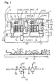
- FIG. 1 (a), (b) and (c) and FIG. 2 show an embodiment of the invention.
- the transistors Tr1 and Tr2 and the free-wheel diodes D1 and D2 are mounted on the pattern parts 3a and 3b formed separately on the circuit substrate in the same way as in FIG. 5.
- the external connection terminals 6 (C1) and 7 (C2E1) are taken out from the pattern parts 3a and 3b, respectively, and the external connection terminal 8 (E2) for the transistor Tr2 is connected to the emitter pattern part 3c which is connected to the emitter electrode of the transistor Tr2 and the anode of the diode D2 by bonding wires 12.
- the auxiliary terminals 9 (e1) and 10 (e2) for the transistors Tr1 and Tr2 are taken out from pattern parts 3f and 3g which are formed separately from the aforementioned pattern parts.
- leads 11 (aluminum wires) connect these pattern parts 3f and 3g to wiring inductance regions of the emitter pattern parts 3e and 3c, respectively.
- slits 14 are cut into the emitter pattern parts 3c and 3e such as to form a hairpin shaped (U-shaped) structure for the current paths. Bonding wires 12 taken out from the respective diode and transistor are bonded onto the one side of this hairpin structure.
- this hairpin structure provides an internal wiring inductance of a desired value.
- leads 11 these inductance regions are connected to the pattern parts 3f and 3g, respectively.
- One end of each lead 11 is bonded within the respective inductance region at a position such that wiring inductances I1 and I2 having the desired values are obtained.
- Slight changes can be made in the values of the wiring inductances I1 and I2 by shifting the position at which the respective lead 11 is connected along the current paths formed in the pattern parts 3c and 3e.
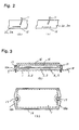
- positioning marks 15 which are easy to see, are provided at equal intervals along the inductance regions to indicate experimentally determined positions for the connection of the lead 11. Since such positioning marks can be easily recognized, desired connecting positions for the bonding work can be easily instructed.
- FIG. 2(a) and (b) Specific examples of these marks 15 are shown in FIG. 2(a) and (b). In FIG. 2(a) equally spaced round holes are formed along the inductance region of the pattern parts 3c and 3e and in FIG. 2(b) equally spaced slits are formed along the edge of the pattern parts 3c and 3e. In both examples the marks are used as indices for indicating or recognizing the bonding position for the lead 11 being bonded.
- Providing the wiring inductances I1 and I2 at the emitter pattern part for each of the transistors as in this embodiment has the following benefits.
- the desired inductances I1 and I2 are provided by an internal connecting member formed at an external connection terminal or as a separate bridge shaped internal connecting member, it is necessary for the shape of the connecting member or the terminal itself to be newly designed and manufactured each time there is a change in the characteristics of the transistors which requires a change in the value of the wiring inductance.
- the appropriate internal wiring inductance can be obtained simply by varying the connecting position of the lead on the circuit pattern.
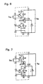
- FIG. 4(a) and (b) show a modification of the examples of FIG. 1.
- the external connection terminal E2 for the transistor Tr2 is on the emitter pattern part 3c, and is taken out from a point which is directly adjacent to the auxiliary terminal e2 connected to the inductance region.
- the wiring inductance between the external connection terminal E2 and the auxiliary terminal e2 becomes almost zero.
- the inductance distribution of the wiring circuits on both sides of the transistor Tr1 in the upper arm is equal to that of the transistor Tr2 in the lower arm . This gives better balance and enhanced stability to the switching characteristics for the transistors Tr1 and Tr2.
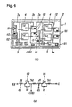
- FIG. 3(a) and (b) A package structure suitable for use with the power transistor modules of each of the embodiments described above is shown in FIG. 3(a) and (b).
- the package is made up of a metal base 1 on which the circuit assembly of each of the embodiments (comprising elements such as the transistors, the free-wheel diodes and external connection terminals) is provided with a circuit substrate between them, and a resin case 16. It is then fixed in place on a heatsink such as a cooling block fin via fixing screws 17 when used. The resin case 16 is then filled up with sealing resin 19 to protect the elements such as the semiconductor chips.
- the outer edge of the metal base 1 is laid onto a stepped peripheral edge part 16a of the resin case 16 where it is glued with adhesive. Moreover, slots are formed on both sides of both the metal base 1 and the resin case 16, as can be seen in FIG. 3(b), so that the two members can then be screwed together by screws 17.
- the bottom of the metal base 1 closely contacts the upper surface of the heatsink 18 when the package of the transistor module is attached to the heatsink 18 with the metal base 1 and the resin case 16 fastened together through the fastening screws 17. Therefore there is no fear that the fitting of the metal base 1 and the resin case 16 will be separated.
- the metal base 1 is required only to have a minimum external dimension necessary for mounting of the internal circuit structure, material can be saved.
- a half bridge circuit assembly comprising two power transistor chips Tr1 and Tr2 (or two pairs of power transistor chips) internally connected together in series is incorporated in a single package.
- two or more half bridge circuit assemblies could be incorporated in the same package with each of the half bridge sections connected together internally so as to provide a single phase full bridge or a three phase full bridge circuit made up of, for example, four, or six power transistor modules.
- a wiring inductance I1 is connected in series between each of the transistors Tr1 and Tr2, with an auxiliary emitter terminal e1 for the transistor Tr1 being taken out from this inductance I1.
- the emitter current 1e flows to the load L through the wiring inductance I1.
- a free-wheeling current If flows from the external connection terminal C2E1 to the load L without flowing through the wiring inductance I1.
- the value for the wiring inductances I1 and I2 is in the order of a few nH to 10 nH which may be provided by utilizing the self-inductance of a conducting (copper) bar of the internal connecting member or a circuit pattern for the circuit substrate.
- the actual effects of the wiring inductance may be confirmed by experiment.
- FIG. 8 (a), (b) and (c) illustrate waveforms of the voltage and current in the main circuit during switching.
- FIG. 8(a) shows the operating waveform for the transistor Tr2 of the lower arm
- FIG. 8(b) shows the operating waveform for the transistor Tr1 of the upper arm of the construction in this embodiment
- FIG. 8(c) shows the operating waveform for the transistor Tr1 in the prior art construction shown in FIG. 5.
Landscapes
- Engineering & Computer Science (AREA)
- Power Engineering (AREA)
- Inverter Devices (AREA)
- Power Conversion In General (AREA)
- Electronic Switches (AREA)
- Semiconductor Integrated Circuits (AREA)
Claims (4)
- Module de transistor à puissance comportant :un substrat (2) de circuit,au moins une paire de puces (Tr1, Tr2) de transistor à puissance montées sur le substrat de circuit et chaque puce de transistor ayant une électrode de collecteur, une électrode d'émetteur et une électrode de grille,une diode (D1, D2) à roue libre connectée de manière antiparallèle aux électrodes d'émetteur et de collecteur de chaque puce de transistor à puissance,une configuration (3) de circuit sur le substrat (2) de circuit formée d'une pluralité de parties de configuration séparées les unes des autres et comportant une première partie (3e) de configuration d'émetteur, une première partie (3a) de configuration de collecteur et une première partie de configuration de grille pour la connexion à l'électrode d'émetteur, à l'électrode de collecteur et à l'électrode de grille respectivement de la première puce (Tr1) de transistor, une deuxième partie (3c) de configuration d'émetteur, une deuxième partie (3b) de configuration de collecteur et une deuxième partie de configuration de grille pour une connexion à l'électrode d'émetteur, à l'électrode de collecteur et à l'électrode de grille respectivement de la deuxième puce (Tr2) de transistor, et une partie de configuration de connexion interne connectant intégralement la première partie de configuration d'émetteur et la deuxième partie de configuration de collecteur de manière à former les bras supérieur et inférieur d'un circuit en pont,des première (C1), deuxième (C2E1) et troisième (E2) bornes de sortie connectées à la première partie (3a) de configuration de collecteur, à la deuxième partie (3b) de configuration de collecteur et à la deuxième partie (3c) de configuration d'émetteur respectivement, et des première et deuxième bornes (G1, G2) de grille connectées aux première et deuxième parties de configuration de grille respectivement,des première et deuxième bornes (e1, e2) auxiliaires qui sortent des première et deuxième parties (3f, 3g) de configuration auxiliaires respectivement, les première et deuxième parties de configuration auxiliaires étant formées séparément à partir de toutes les parties de configuration précédemment définies, les première et deuxième bornes (e1, e2) auxiliaires étant connectées aux parties de configuration auxquelles les deuxième et troisièmes bornes (C2E1, E2) de sortie sont connectées en utilisant une inductance de câblage formée par la configuration de circuit entre l'électrode d'émetteur de la première puce de transistor et la première borne auxiliaire, d'une part, et entre l'électrode d'émetteur de la deuxième puce de transistor et la deuxième borne auxiliaire, d'autre part,la première partie (3e) de configuration d'émetteur étant divisée par une fente de manière à former une structure en forme de U avec un premier jambage auquel l'électrode d'émetteur de la première puce (Tr1) de transistor est connectée et un deuxième jambage auquel la première borne (e1) auxiliaire est connectée, la partie de configuration de connexion intérieure connectant l'extrémité libre du deuxième jambage à la deuxième partie (3b) de configuration de collecteur, etla deuxième partie (3c) de configuration d'émetteur est divisée par une fente de manière à former une structure en forme de U avec un premier jambage auquel l'électrode d'émetteur de la deuxième puce (Tr2) de transistor est connectée et un deuxième jambage auquel la deuxième borne (e2) auxiliaire est connectée, la troisième borne (E2) de sortie étant connectée au deuxième jambage.
- Module suivant la revendication 1, dans lequel des repères (15) de positionnement indiquant des positions pour la connexion des bornes (e1, e2) auxiliaires sont disposés le long du deuxième jambage, chaque repère correspondant à une autre valeur de l'inductance de câblage.
- Module suivant la revendication 1 ou 2, comportant en outre une partie (3f, 3g) de configuration auxiliaire connectée par un conducteur (11) au deuxième jambage, les bornes (e1, e2) auxiliaires étant connectées à la partie (3f, 3g) de configuration auxiliaire.
- Module suivant l'une quelconque des revendications 1 à 3, dans lequel la position de connexion pour la troisième borne (E2) de connexion extérieure à la deuxième partie (3c) de configuration d'émetteur est proche de la position de connexion pour la deuxième borne (e2) auxiliaire.
Applications Claiming Priority (10)
| Application Number | Priority Date | Filing Date | Title |
|---|---|---|---|
| JP97434/93 | 1993-04-23 | ||
| JP9743493 | 1993-04-23 | ||
| JP9743493 | 1993-04-23 | ||
| JP18426793 | 1993-07-27 | ||
| JP18426793 | 1993-07-27 | ||
| JP184267/93 | 1993-07-27 | ||
| JP5269353A JP2973799B2 (ja) | 1993-04-23 | 1993-10-28 | パワートランジスタモジュール |
| JP26935393 | 1993-10-28 | ||
| JP269353/93 | 1993-10-28 | ||
| EP94106178A EP0621635A1 (fr) | 1993-04-23 | 1994-04-21 | Module à transistor de puissance |
Related Parent Applications (2)
| Application Number | Title | Priority Date | Filing Date |
|---|---|---|---|
| EP94106178A Division EP0621635A1 (fr) | 1993-04-23 | 1994-04-21 | Module à transistor de puissance |
| EP94106178.0 Division | 1994-04-21 |
Publications (3)
| Publication Number | Publication Date |
|---|---|
| EP0809292A2 EP0809292A2 (fr) | 1997-11-26 |
| EP0809292A3 EP0809292A3 (fr) | 1998-01-28 |
| EP0809292B1 true EP0809292B1 (fr) | 2002-07-31 |
Family
ID=27308400
Family Applications (2)
| Application Number | Title | Priority Date | Filing Date |
|---|---|---|---|
| EP94106178A Withdrawn EP0621635A1 (fr) | 1993-04-23 | 1994-04-21 | Module à transistor de puissance |
| EP97112462A Expired - Lifetime EP0809292B1 (fr) | 1993-04-23 | 1994-04-21 | Module de transistor à puissance |
Family Applications Before (1)
| Application Number | Title | Priority Date | Filing Date |
|---|---|---|---|
| EP94106178A Withdrawn EP0621635A1 (fr) | 1993-04-23 | 1994-04-21 | Module à transistor de puissance |
Country Status (4)
| Country | Link |
|---|---|
| US (1) | US5616955A (fr) |
| EP (2) | EP0621635A1 (fr) |
| JP (1) | JP2973799B2 (fr) |
| DE (1) | DE69431128T2 (fr) |
Cited By (1)
| Publication number | Priority date | Publication date | Assignee | Title |
|---|---|---|---|---|
| DE10219760A1 (de) * | 2002-05-02 | 2003-11-20 | Eupec Gmbh & Co Kg | Halbbrückenschaltung |
Families Citing this family (57)
| Publication number | Priority date | Publication date | Assignee | Title |
|---|---|---|---|---|
| EP0689246B1 (fr) * | 1994-05-27 | 2003-08-27 | Texas Instruments Incorporated | Améliorations concernant des dispositifs semi-conducteurs |
| US5956231A (en) * | 1994-10-07 | 1999-09-21 | Hitachi, Ltd. | Semiconductor device having power semiconductor elements |
| JP3480771B2 (ja) * | 1995-12-20 | 2003-12-22 | 三菱電機株式会社 | 半導体装置 |
| JP3476612B2 (ja) * | 1995-12-21 | 2003-12-10 | 三菱電機株式会社 | 半導体装置 |
| US6404045B1 (en) * | 1996-02-01 | 2002-06-11 | International Rectifier Corporation | IGBT and free-wheeling diode combination |
| US5726862A (en) * | 1996-02-02 | 1998-03-10 | Motorola, Inc. | Electrical component having formed leads |
| US6954368B1 (en) | 1996-07-22 | 2005-10-11 | HYDRO-QUéBEC | Low stray interconnection inductance power converting molecule for converting a DC voltage into an AC voltage, and a method therefor |
| DE19722355A1 (de) * | 1997-05-28 | 1998-12-03 | Bosch Gmbh Robert | Verfahren zur Herstellung elektrischer Baugruppen und elektrische Baugruppe |
| US6060772A (en) * | 1997-06-30 | 2000-05-09 | Kabushiki Kaisha Toshiba | Power semiconductor module with a plurality of semiconductor chips |
| FR2776462B1 (fr) * | 1998-03-19 | 2000-05-19 | Schneider Electric Sa | Module de composants electroniques de puissance |
| US5895974A (en) * | 1998-04-06 | 1999-04-20 | Delco Electronics Corp. | Durable substrate subassembly for transistor switch module |
| US6054765A (en) * | 1998-04-27 | 2000-04-25 | Delco Electronics Corporation | Parallel dual switch module |
| JP3552549B2 (ja) * | 1998-09-08 | 2004-08-11 | 株式会社豊田自動織機 | 半導体モジュールの電極端子接続構造 |
| JP2000208181A (ja) * | 1999-01-08 | 2000-07-28 | Aisin Aw Co Ltd | 電子部品及びその製造装置 |
| DE19935100B4 (de) * | 1999-07-27 | 2004-10-28 | Infineon Technologies Ag | Halbbrückenkonfiguration |
| JP3457237B2 (ja) * | 1999-11-10 | 2003-10-14 | 株式会社オートネットワーク技術研究所 | 電気接続箱の回路接続構造及び回路形成方法 |
| US6422901B1 (en) | 1999-12-06 | 2002-07-23 | Fci Americas Technology, Inc. | Surface mount device and use thereof |
| US6417532B2 (en) * | 2000-01-28 | 2002-07-09 | Kabushiki Kaisha Toshiba | Power semiconductor module for use in power conversion units with downsizing requirements |
| JP3073273U (ja) * | 2000-05-16 | 2000-11-14 | 船井電機株式会社 | 光ピックアップ装置 |
| US20020024134A1 (en) * | 2000-08-28 | 2002-02-28 | Mitsubishi Denki Kabushiki Kaisha | Semiconductor device |
| JP4484400B2 (ja) * | 2000-08-28 | 2010-06-16 | 三菱電機株式会社 | 半導体装置 |
| JP3923716B2 (ja) * | 2000-09-29 | 2007-06-06 | 株式会社東芝 | 半導体装置 |
| JP2003009508A (ja) * | 2001-06-19 | 2003-01-10 | Mitsubishi Electric Corp | 電力用半導体装置 |
| US6885562B2 (en) * | 2001-12-28 | 2005-04-26 | Medtronic Physio-Control Manufacturing Corporation | Circuit package and method for making the same |
| KR20040085169A (ko) * | 2002-01-29 | 2004-10-07 | 어드밴스드 파워 테크놀로지 인코포레이티드 | 스플릿 게이트 파워 모듈과 그 모듈안의 진동을 억제하는방법 |
| KR100873417B1 (ko) * | 2002-04-16 | 2008-12-11 | 페어차일드코리아반도체 주식회사 | 최적화된 dbc 패턴 및 단자 구조를 갖는 전력용 반도체모듈 |
| DE10230156A1 (de) * | 2002-07-04 | 2004-01-22 | eupec Europäische Gesellschaft für Leistungshalbleiter mbH | Leistungshalbleitermodul und Schaltungsanordnung |
| DE10334079B4 (de) * | 2003-07-25 | 2008-08-21 | Siemens Ag | Transistormodul |
| DE102004027185B4 (de) * | 2004-06-03 | 2008-08-28 | Infineon Technologies Ag | Niederinduktives Halbleiterbauelement mit Halbbrückenkonfiguration |
| US7227198B2 (en) * | 2004-08-11 | 2007-06-05 | International Rectifier Corporation | Half-bridge package |
| CN100373617C (zh) * | 2004-11-08 | 2008-03-05 | 吴才荣 | 一种配对晶体管及其制造方法 |
| JP2006253516A (ja) * | 2005-03-14 | 2006-09-21 | Hitachi Ltd | パワー半導体装置 |
| DE102005039478B4 (de) * | 2005-08-18 | 2007-05-24 | Infineon Technologies Ag | Leistungshalbleiterbauteil mit Halbleiterchipstapel und Verfahren zur Herstellung desselben |
| JP2007209184A (ja) * | 2006-02-06 | 2007-08-16 | Mitsubishi Electric Corp | 電力変換装置 |
| JP4537370B2 (ja) * | 2006-12-04 | 2010-09-01 | 日立オートモティブシステムズ株式会社 | 電子装置 |
| DE102007029657B4 (de) * | 2007-06-27 | 2017-10-19 | Fuji Electric Co., Ltd. | Wechselrichtermodul für Stromrichter |
| SI2340560T1 (sl) | 2008-01-25 | 2014-02-28 | Letrika Lab D.O.O. | Močnostni stikalni modul |
| US8493762B2 (en) * | 2009-12-28 | 2013-07-23 | Kabushiki Kaisha Toshiba | Power semiconductor module and semiconductor power converter provided with the same |
| EP2750187B1 (fr) * | 2011-08-25 | 2020-01-01 | Fuji Electric Co., Ltd. | Dispositif à semi-conducteur et procédé de fabrication de dispositif à semi-conducteur |
| JP6065839B2 (ja) * | 2011-09-30 | 2017-01-25 | 富士電機株式会社 | 半導体装置及びその製造方法 |
| CN104380463B (zh) * | 2012-06-19 | 2017-05-10 | Abb 技术有限公司 | 用于将多个功率晶体管安装在其上的衬底和功率半导体模块 |
| JP6041770B2 (ja) * | 2013-08-26 | 2016-12-14 | カルソニックカンセイ株式会社 | 半導体装置 |
| WO2015121015A1 (fr) * | 2014-02-14 | 2015-08-20 | Abb Technology Ag | Module à semi-conducteur à deux chemins conducteurs d'émetteur auxiliaires |
| CN106489203B (zh) | 2014-07-03 | 2018-09-18 | 日产自动车株式会社 | 半桥式功率半导体模块及其制造方法 |
| JP6405383B2 (ja) | 2014-07-15 | 2018-10-17 | 株式会社日立製作所 | パワートランジスタモジュール |
| JP6451747B2 (ja) * | 2014-11-28 | 2019-01-16 | 富士電機株式会社 | 半導体装置 |
| JP6288301B2 (ja) * | 2014-11-28 | 2018-03-14 | 日産自動車株式会社 | ハーフブリッジパワー半導体モジュール及びその製造方法 |
| JP6447391B2 (ja) * | 2015-06-30 | 2019-01-09 | オムロン株式会社 | 電力変換装置 |
| JP6468984B2 (ja) | 2015-10-22 | 2019-02-13 | 三菱電機株式会社 | 半導体装置 |
| US10340811B2 (en) | 2016-11-28 | 2019-07-02 | Ford Global Technologies, Llc | Inverter switching devices with gate coils to enhance common source inductance |
| JP6390807B1 (ja) * | 2018-03-02 | 2018-09-19 | 富士電機株式会社 | 電力変換装置 |
| US10862232B2 (en) * | 2018-08-02 | 2020-12-08 | Dell Products L.P. | Circuit board pad connector system |
| WO2020071102A1 (fr) | 2018-10-05 | 2020-04-09 | 富士電機株式会社 | Dispositif à semi-conducteur, module à semi-conducteur et véhicule |
| CN112514066B (zh) * | 2019-02-18 | 2025-01-24 | 富士电机株式会社 | 半导体装置 |
| CN116057691A (zh) | 2021-02-12 | 2023-05-02 | 富士电机株式会社 | 半导体模块 |
| DE102021117924B4 (de) * | 2021-07-12 | 2024-05-29 | Danfoss Silicon Power Gmbh | Leistungsmodul |
| JP7555890B2 (ja) * | 2021-09-16 | 2024-09-25 | 株式会社東芝 | 半導体装置 |
Citations (2)
| Publication number | Priority date | Publication date | Assignee | Title |
|---|---|---|---|---|
| EP0455322A1 (fr) * | 1990-02-23 | 1991-11-06 | Fuji Electric Co. Ltd. | Dispositif semi-conducteur |
| EP0527033A2 (fr) * | 1991-08-06 | 1993-02-10 | Fuji Electric Co. Ltd. | Module semi-conducteur |
Family Cites Families (8)
| Publication number | Priority date | Publication date | Assignee | Title |
|---|---|---|---|---|
| JPS5968958A (ja) * | 1982-10-12 | 1984-04-19 | Mitsubishi Electric Corp | ゲ−トタ−ンオフサイリスタ組立体 |
| JPS60239051A (ja) * | 1984-05-11 | 1985-11-27 | Mitsubishi Electric Corp | 半導体装置 |
| US4920405A (en) * | 1986-11-28 | 1990-04-24 | Fuji Electric Co., Ltd. | Overcurrent limiting semiconductor device |
| DE3937045A1 (de) * | 1989-11-07 | 1991-05-08 | Abb Ixys Semiconductor Gmbh | Leistungshalbleitermodul |
| US5243217A (en) * | 1990-11-03 | 1993-09-07 | Fuji Electric Co., Ltd. | Sealed semiconductor device with protruding portion |
| JP2850606B2 (ja) * | 1991-11-25 | 1999-01-27 | 富士電機株式会社 | トランジスタモジュール |
| DE9203000U1 (de) * | 1992-03-06 | 1992-06-17 | Siemens AG, 8000 München | Halbleiteranordnung mit mehreren Halbleiterkörpern |
| JP3053298B2 (ja) * | 1992-08-19 | 2000-06-19 | 株式会社東芝 | 半導体装置 |
-
1993
- 1993-10-28 JP JP5269353A patent/JP2973799B2/ja not_active Expired - Fee Related
-
1994
- 1994-04-21 EP EP94106178A patent/EP0621635A1/fr not_active Withdrawn
- 1994-04-21 EP EP97112462A patent/EP0809292B1/fr not_active Expired - Lifetime
- 1994-04-21 DE DE69431128T patent/DE69431128T2/de not_active Expired - Lifetime
- 1994-04-22 US US08/231,338 patent/US5616955A/en not_active Expired - Lifetime
Patent Citations (2)
| Publication number | Priority date | Publication date | Assignee | Title |
|---|---|---|---|---|
| EP0455322A1 (fr) * | 1990-02-23 | 1991-11-06 | Fuji Electric Co. Ltd. | Dispositif semi-conducteur |
| EP0527033A2 (fr) * | 1991-08-06 | 1993-02-10 | Fuji Electric Co. Ltd. | Module semi-conducteur |
Cited By (1)
| Publication number | Priority date | Publication date | Assignee | Title |
|---|---|---|---|---|
| DE10219760A1 (de) * | 2002-05-02 | 2003-11-20 | Eupec Gmbh & Co Kg | Halbbrückenschaltung |
Also Published As
| Publication number | Publication date |
|---|---|
| EP0809292A3 (fr) | 1998-01-28 |
| EP0621635A1 (fr) | 1994-10-26 |
| EP0809292A2 (fr) | 1997-11-26 |
| DE69431128D1 (de) | 2002-09-05 |
| US5616955A (en) | 1997-04-01 |
| JP2973799B2 (ja) | 1999-11-08 |
| JPH0799275A (ja) | 1995-04-11 |
| DE69431128T2 (de) | 2003-02-13 |
Similar Documents
| Publication | Publication Date | Title |
|---|---|---|
| EP0809292A2 (fr) | Module de transistor à puissance | |
| US5466969A (en) | Intelligent power device module | |
| JP7642714B2 (ja) | 半導体装置 | |
| US5705848A (en) | Power semiconductor module having a plurality of submodules | |
| US9773767B2 (en) | Semiconductor device | |
| US11923266B2 (en) | Semiconductor module circuit structure | |
| US5202578A (en) | Module-type semiconductor device of high power capacity | |
| JP4196001B2 (ja) | 半導体パワーモジュール | |
| US20240290698A1 (en) | Power semiconductor module and power conversion device | |
| US7279963B2 (en) | Low inductance semiconductor device having half-bridge configuration | |
| JP7831463B2 (ja) | 半導体モジュール及び半導体装置 | |
| US6795324B2 (en) | Power converter | |
| JP7438021B2 (ja) | 半導体装置 | |
| EP0455322B1 (fr) | Dispositif semi-conducteur | |
| US11145558B2 (en) | Manufacturing method of semiconductor module | |
| US20230078823A1 (en) | Semiconductor device | |
| US6232654B1 (en) | Semiconductor module | |
| JP4246040B2 (ja) | 半導体装置の実装体 | |
| JP2580804B2 (ja) | 電力変換装置用トランジスタモジュール | |
| Stockmeier et al. | Novel high power semiconductor module for trench IGBTs | |
| JP2580803B2 (ja) | 電力変換装置用トランジスタモジュール | |
| WO2023145144A1 (fr) | Module semi-conducteur de puissance | |
| JP2580798B2 (ja) | 電力変換装置用トランジスタモジュール | |
| JP6373901B2 (ja) | 高効率モジュール | |
| KR100419051B1 (ko) | 반도체장치 |
Legal Events
| Date | Code | Title | Description |
|---|---|---|---|
| PUAI | Public reference made under article 153(3) epc to a published international application that has entered the european phase |
Free format text: ORIGINAL CODE: 0009012 |
|
| 17P | Request for examination filed |
Effective date: 19970721 |
|
| AC | Divisional application: reference to earlier application |
Ref document number: 621635 Country of ref document: EP |
|
| AK | Designated contracting states |
Kind code of ref document: A2 Designated state(s): DE FR GB |
|
| PUAL | Search report despatched |
Free format text: ORIGINAL CODE: 0009013 |
|
| AK | Designated contracting states |
Kind code of ref document: A3 Designated state(s): DE FR GB |
|
| 17Q | First examination report despatched |
Effective date: 19990901 |
|
| GRAG | Despatch of communication of intention to grant |
Free format text: ORIGINAL CODE: EPIDOS AGRA |
|
| GRAG | Despatch of communication of intention to grant |
Free format text: ORIGINAL CODE: EPIDOS AGRA |
|
| GRAH | Despatch of communication of intention to grant a patent |
Free format text: ORIGINAL CODE: EPIDOS IGRA |
|
| GRAH | Despatch of communication of intention to grant a patent |
Free format text: ORIGINAL CODE: EPIDOS IGRA |
|
| GRAA | (expected) grant |
Free format text: ORIGINAL CODE: 0009210 |
|
| AC | Divisional application: reference to earlier application |
Ref document number: 621635 Country of ref document: EP |
|
| AK | Designated contracting states |
Kind code of ref document: B1 Designated state(s): DE FR GB |
|
| REG | Reference to a national code |
Ref country code: GB Ref legal event code: FG4D |
|
| REF | Corresponds to: |
Ref document number: 69431128 Country of ref document: DE Date of ref document: 20020905 |
|
| ET | Fr: translation filed | ||
| PLBE | No opposition filed within time limit |
Free format text: ORIGINAL CODE: 0009261 |
|
| STAA | Information on the status of an ep patent application or granted ep patent |
Free format text: STATUS: NO OPPOSITION FILED WITHIN TIME LIMIT |
|
| 26N | No opposition filed |
Effective date: 20030506 |
|
| REG | Reference to a national code |
Ref country code: GB Ref legal event code: 746 Effective date: 20050411 |
|
| REG | Reference to a national code |
Ref country code: FR Ref legal event code: D6 |
|
| PGFP | Annual fee paid to national office [announced via postgrant information from national office to epo] |
Ref country code: FR Payment date: 20060410 Year of fee payment: 13 |
|
| PG25 | Lapsed in a contracting state [announced via postgrant information from national office to epo] |
Ref country code: FR Free format text: LAPSE BECAUSE OF NON-PAYMENT OF DUE FEES Effective date: 20070430 |
|
| PGFP | Annual fee paid to national office [announced via postgrant information from national office to epo] |
Ref country code: GB Payment date: 20090415 Year of fee payment: 16 |
|
| GBPC | Gb: european patent ceased through non-payment of renewal fee |
Effective date: 20100421 |
|
| PG25 | Lapsed in a contracting state [announced via postgrant information from national office to epo] |
Ref country code: GB Free format text: LAPSE BECAUSE OF NON-PAYMENT OF DUE FEES Effective date: 20100421 |
|
| REG | Reference to a national code |
Ref country code: DE Ref legal event code: R082 Ref document number: 69431128 Country of ref document: DE Representative=s name: HOFFMANN, ECKART, DIPL.-ING., DE Effective date: 20110826 Ref country code: DE Ref legal event code: R081 Ref document number: 69431128 Country of ref document: DE Owner name: FUJI ELECTRIC CO., LTD., JP Free format text: FORMER OWNER: FUJI ELECTRIC SYSTEMS CO., LTD., TOKYO/TOKIO, JP Effective date: 20110826 |
|
| PGFP | Annual fee paid to national office [announced via postgrant information from national office to epo] |
Ref country code: DE Payment date: 20130508 Year of fee payment: 20 |
|
| REG | Reference to a national code |
Ref country code: DE Ref legal event code: R071 Ref document number: 69431128 Country of ref document: DE |
|
| PG25 | Lapsed in a contracting state [announced via postgrant information from national office to epo] |
Ref country code: DE Free format text: LAPSE BECAUSE OF EXPIRATION OF PROTECTION Effective date: 20140423 |