EP0810609A2 - Einzelelektron-Speicherzellenanordnung - Google Patents
Einzelelektron-Speicherzellenanordnung Download PDFInfo
- Publication number
- EP0810609A2 EP0810609A2 EP97107314A EP97107314A EP0810609A2 EP 0810609 A2 EP0810609 A2 EP 0810609A2 EP 97107314 A EP97107314 A EP 97107314A EP 97107314 A EP97107314 A EP 97107314A EP 0810609 A2 EP0810609 A2 EP 0810609A2
- Authority
- EP
- European Patent Office
- Prior art keywords
- tunnel
- electron
- memory cell
- line
- voltage
- Prior art date
- Legal status (The legal status is an assumption and is not a legal conclusion. Google has not performed a legal analysis and makes no representation as to the accuracy of the status listed.)
- Granted
Links
- 238000003860 storage Methods 0.000 claims abstract description 50
- 230000001419 dependent effect Effects 0.000 claims abstract description 3
- 229910052751 metal Inorganic materials 0.000 description 7
- 239000002184 metal Substances 0.000 description 7
- 230000008859 change Effects 0.000 description 6
- 238000012546 transfer Methods 0.000 description 5
- RTAQQCXQSZGOHL-UHFFFAOYSA-N Titanium Chemical compound [Ti] RTAQQCXQSZGOHL-UHFFFAOYSA-N 0.000 description 4
- 229910052782 aluminium Inorganic materials 0.000 description 4
- XAGFODPZIPBFFR-UHFFFAOYSA-N aluminium Chemical compound [Al] XAGFODPZIPBFFR-UHFFFAOYSA-N 0.000 description 4
- 239000003990 capacitor Substances 0.000 description 4
- PCHJSUWPFVWCPO-UHFFFAOYSA-N gold Chemical compound [Au] PCHJSUWPFVWCPO-UHFFFAOYSA-N 0.000 description 4
- 229910052737 gold Inorganic materials 0.000 description 4
- 239000010931 gold Substances 0.000 description 4
- 238000000034 method Methods 0.000 description 4
- 230000008569 process Effects 0.000 description 4
- 239000010936 titanium Substances 0.000 description 4
- 229910052719 titanium Inorganic materials 0.000 description 4
- 230000007704 transition Effects 0.000 description 4
- 230000003647 oxidation Effects 0.000 description 3
- 238000007254 oxidation reaction Methods 0.000 description 3
- 238000000151 deposition Methods 0.000 description 2
- 238000010586 diagram Methods 0.000 description 2
- 230000000694 effects Effects 0.000 description 2
- 238000009413 insulation Methods 0.000 description 2
- 238000005036 potential barrier Methods 0.000 description 2
- 239000000758 substrate Substances 0.000 description 2
- XMWRBQBLMFGWIX-UHFFFAOYSA-N C60 fullerene Chemical class C12=C3C(C4=C56)=C7C8=C5C5=C9C%10=C6C6=C4C1=C1C4=C6C6=C%10C%10=C9C9=C%11C5=C8C5=C8C7=C3C3=C7C2=C1C1=C2C4=C6C4=C%10C6=C9C9=C%11C5=C5C8=C3C3=C7C1=C1C2=C4C6=C2C9=C5C3=C12 XMWRBQBLMFGWIX-UHFFFAOYSA-N 0.000 description 1
- 101100116570 Caenorhabditis elegans cup-2 gene Proteins 0.000 description 1
- 101100116572 Drosophila melanogaster Der-1 gene Proteins 0.000 description 1
- 229910001218 Gallium arsenide Inorganic materials 0.000 description 1
- 229910004298 SiO 2 Inorganic materials 0.000 description 1
- XUIMIQQOPSSXEZ-UHFFFAOYSA-N Silicon Chemical compound [Si] XUIMIQQOPSSXEZ-UHFFFAOYSA-N 0.000 description 1
- 238000003491 array Methods 0.000 description 1
- 230000006399 behavior Effects 0.000 description 1
- 230000008901 benefit Effects 0.000 description 1
- 230000000903 blocking effect Effects 0.000 description 1
- 239000004020 conductor Substances 0.000 description 1
- 230000007423 decrease Effects 0.000 description 1
- 230000008021 deposition Effects 0.000 description 1
- 238000005516 engineering process Methods 0.000 description 1
- 229910003472 fullerene Inorganic materials 0.000 description 1
- 238000011835 investigation Methods 0.000 description 1
- 238000001459 lithography Methods 0.000 description 1
- 238000004519 manufacturing process Methods 0.000 description 1
- 238000005259 measurement Methods 0.000 description 1
- 238000004377 microelectronic Methods 0.000 description 1
- 238000005442 molecular electronic Methods 0.000 description 1
- 239000013110 organic ligand Substances 0.000 description 1
- 238000012856 packing Methods 0.000 description 1
- 238000001020 plasma etching Methods 0.000 description 1
- 230000005855 radiation Effects 0.000 description 1
- 239000000523 sample Substances 0.000 description 1
- 229910052594 sapphire Inorganic materials 0.000 description 1
- 239000010980 sapphire Substances 0.000 description 1
- 229910052710 silicon Inorganic materials 0.000 description 1
- 239000010703 silicon Substances 0.000 description 1
- 239000000126 substance Substances 0.000 description 1
- 230000005469 synchrotron radiation Effects 0.000 description 1
- 230000005641 tunneling Effects 0.000 description 1
Images

Classifications
-
- G—PHYSICS
- G11—INFORMATION STORAGE
- G11C—STATIC STORES
- G11C11/00—Digital stores characterised by the use of particular electric or magnetic storage elements; Storage elements therefor
-
- G—PHYSICS
- G11—INFORMATION STORAGE
- G11C—STATIC STORES
- G11C11/00—Digital stores characterised by the use of particular electric or magnetic storage elements; Storage elements therefor
- G11C11/21—Digital stores characterised by the use of particular electric or magnetic storage elements; Storage elements therefor using electric elements
- G11C11/34—Digital stores characterised by the use of particular electric or magnetic storage elements; Storage elements therefor using electric elements using semiconductor devices
- G11C11/40—Digital stores characterised by the use of particular electric or magnetic storage elements; Storage elements therefor using electric elements using semiconductor devices using transistors
- G11C11/401—Digital stores characterised by the use of particular electric or magnetic storage elements; Storage elements therefor using electric elements using semiconductor devices using transistors forming cells needing refreshing or charge regeneration, i.e. dynamic cells
- G11C11/403—Digital stores characterised by the use of particular electric or magnetic storage elements; Storage elements therefor using electric elements using semiconductor devices using transistors forming cells needing refreshing or charge regeneration, i.e. dynamic cells with charge regeneration common to a multiplicity of memory cells, i.e. external refresh
- G11C11/404—Digital stores characterised by the use of particular electric or magnetic storage elements; Storage elements therefor using electric elements using semiconductor devices using transistors forming cells needing refreshing or charge regeneration, i.e. dynamic cells with charge regeneration common to a multiplicity of memory cells, i.e. external refresh with one charge-transfer gate, e.g. MOS transistor, per cell
-
- B—PERFORMING OPERATIONS; TRANSPORTING
- B82—NANOTECHNOLOGY
- B82Y—SPECIFIC USES OR APPLICATIONS OF NANOSTRUCTURES; MEASUREMENT OR ANALYSIS OF NANOSTRUCTURES; MANUFACTURE OR TREATMENT OF NANOSTRUCTURES
- B82Y10/00—Nanotechnology for information processing, storage or transmission, e.g. quantum computing or single electron logic
-
- G—PHYSICS
- G11—INFORMATION STORAGE
- G11C—STATIC STORES
- G11C2216/00—Indexing scheme relating to G11C16/00 and subgroups, for features not directly covered by these groups
- G11C2216/02—Structural aspects of erasable programmable read-only memories
- G11C2216/08—Nonvolatile memory wherein data storage is accomplished by storing relatively few electrons in the storage layer, i.e. single electron memory
-
- Y—GENERAL TAGGING OF NEW TECHNOLOGICAL DEVELOPMENTS; GENERAL TAGGING OF CROSS-SECTIONAL TECHNOLOGIES SPANNING OVER SEVERAL SECTIONS OF THE IPC; TECHNICAL SUBJECTS COVERED BY FORMER USPC CROSS-REFERENCE ART COLLECTIONS [XRACs] AND DIGESTS
- Y10—TECHNICAL SUBJECTS COVERED BY FORMER USPC
- Y10S—TECHNICAL SUBJECTS COVERED BY FORMER USPC CROSS-REFERENCE ART COLLECTIONS [XRACs] AND DIGESTS
- Y10S977/00—Nanotechnology
- Y10S977/902—Specified use of nanostructure
- Y10S977/932—Specified use of nanostructure for electronic or optoelectronic application
- Y10S977/936—Specified use of nanostructure for electronic or optoelectronic application in a transistor or 3-terminal device
- Y10S977/937—Single electron transistor
Definitions
- Random dynamic access memory cell (DRAM) arrays are currently mainly manufactured using CMOS technology. They include memory cells, each with a read transistor and a capacitor. The information to be stored is stored on the capacitor in the form of a quantity of charge.
- the signal charge is usually around 50 fC, i.e. it consists of 300,000 electrons.
- the capacitance of the capacitor in today's memory cells is 20 to 30 fF.
- the area per memory cell decreases with increasing packing density of future memory arrangements. It is becoming increasingly difficult, if not impossible, to manufacture a capacitor with the relatively large storage capacity of 20 to 30 fF on the area available for the memory cell.
- the read-out transistor cannot be downsized as well.
- Single-electron components include tunnel elements that are connected to adjacent connections via tunnel contacts. Charge transfers via these tunnel contacts take place both via the quantum mechanical tunnel effect and by simply thermally overcoming a potential barrier, these charge transfers occurring sufficiently rarely.
- the tunnel elements are implemented, for example, as small conductive islands surrounded by an insulating structure.
- the single-electron component By controlling the tunnel element via a gate electrode, which capacitively influences the tunnel element without causing tunnel transitions in the operating voltage range, a current flow through the tunnel element is possible. If a suitable electrical charge is effective at the gate electrode, the single-electron component has an approximately linear current-voltage characteristic curve going through the zero point. Such a gate-controlled single-electron component is referred to in the literature as a single-electron transistor.
- a multi-tunnel element is a series connection of tunnel elements which are connected to one another via a tunnel contact.
- the multi-tunnel elements each have a lateral gate electrode, via which a current through the multi-tunnel elements can be controlled.
- a first multi-tunnel element and a second multi-tunnel element are connected in series between a first voltage source and ground.
- the two multi-tunnel elements are connected to one another via a storage node.
- the side gate electrodes of the multi-tunnel elements are connected to a second voltage source and a third voltage source.
- the storage node is connected to a fourth voltage source via a capacitance.
- the storage node is connected via a further capacitance to a third multi-tunnel element which is connected between a fifth voltage source and ground.
- the third multi-tunnel element is also controlled by a side gate electrode which is connected to a sixth voltage source.
- the third multi-tunnel element acts as an electrometer, with which the charge on the storage node is detected. Measurements in which a high negative voltage was applied to the side gate electrode of the second multi-tunnel element have shown that individual electrons can be stored stably in the first multi-tunnel element and in the storage node, provided that the voltage applied to the multi-tunnel element fulfills the condition for Coulomb blockade . Depending on the voltage applied to the side gate electrode, a discrete number of electrons can be stably stored in the storage element formed from the storage node and the first multi-tunnel element.
- the electrostatic energy of the storage element assumes a metastable state for the corresponding number of stored electrons. Between neighboring, metastable states, the electrostatic energy has a potential wall, the apex of which is higher than the next metastable state.
- the height of the potential walls depends on the number of stored electrons and the number of tunnel contacts in the multi-tunnel element.
- the single-electron memory cell is implemented in delta-doped GaAs. Since six voltage sources are required to operate the single-electron memory cell, a memory cell arrangement which comprises a large number of such memory cells can be driven in a complex manner.
- the invention is therefore based on the problem of specifying a single-electron memory cell arrangement which can be controlled with less effort.
- a single-electron memory cell arrangement which comprises memory cells each having a single-electron memory element and a single-electron transistor. Each of the memory cells is connected between a first line and a second line.
- the memory cell arrangement comprises parallel first lines and parallel second lines, the first lines and the second lines running transversely to one another. The first lines and the second lines are comparable to the word and bit lines in current DRAM arrangements.
- each of the memory cells can be easily controlled by applying corresponding voltage levels to the associated first line and the associated second line.
- the single-electron storage element comprises at least one tunnel element which is connected to the first line via a first tunnel contact and to a storage node via a second tunnel contact and which can be controlled capacitively via a first gate electrode.
- Charge transfers occur via the tunnel contacts, both through the quantum mechanical tunnel effect and through sufficiently infrequent thermal overcoming of a potential barrier.
- Is the tunnel resistance R T > R K h / e 2nd ⁇ 26k ⁇ , where R K is the Klitzing resistance, h is the Planck constant and e is an electron charge, the majority of charge transfers occur through elementary processes.
- the tunnel resistance is preferably greater than 100 k ⁇ , so that the elementary processes predominate when the charge is transferred.
- the first gate electrode is with the second line connected.
- the single-electron transistor is connected to the first line via a first connection and to the second line via a second connection. It can be controlled capacitively via a second gate electrode, which is connected to the storage node.
- the capacitances of the memory element and the single-electron transistor are coordinated such that when a read voltage is applied by the single-electron transistor, a current which is dependent on a charge stored in the memory element flows.
- the charge stored in the storage element is not changed.
- a write voltage that is greater in magnitude than the read voltage, however, the charge stored in the memory element can be changed.
- the invention makes use of the knowledge that a single-electron transistor is a sensitive electrometer for a charge effective at the gate electrode of the single-electron transistor.
- the read voltage is selected so that the condition for Coulomb blockade is met.
- the current flowing through the single-electron transistor depends on the charge on the storage node, since the storage node is connected to the second gate electrode of the single-electron transistor. At the same time, a change in the charge stored on the storage node is prevented by the fact that the reading voltage applied to the first gate electrode is insufficient to change the electrical charge on the storage node.
- the capacitances of the single-electron storage element and the single-electron transistor are coordinated with one another in such a way that, when the reading voltage for the single-electron transistor is present, at the same time the condition for Coulomb blockade is fulfilled and a change in the state of charge of the single-electron storage element is not possible. With the higher write voltage, however, a change in the state of charge of the storage node is brought about.
- a voltage level corresponding to the read voltage is applied between the associated first line and second line.
- the remaining first lines and second lines are connected to the same potential as the selected first line, so that all cells that do not belong to the selected second line are voltage-free.
- a voltage level corresponding to the write voltage is applied between the associated first line and second line.
- the remaining first lines and second lines are connected in such a way that a lower voltage level drops across the remaining memory cells, at which no change in the stored charge occurs.
- a voltage level corresponding to the reading voltage or the difference between writing and reading voltage can be applied to the other lines, for example.
- the capacitances of the memory element and the single-electron transistor are preferably matched such that the magnitude of the read voltage is half the magnitude of the magnitude of the write voltage.
- the remaining first lines and the second lines can be supplied with the read voltage and the same voltage always drops across a part of the non-selected memory cells.
- the remaining unselected memory cells are voltage-free.
- the storage element preferably comprises a plurality of tunnel elements which are connected to one another in each case as a row via tunnel contacts. This applies to the properties of these tunnel contacts in relation to the first tunnel contact and the second tunnel contact said.
- the first tunnel element is connected to the first line via the first tunnel contact and the last tunnel element in the row is connected to the storage node via the second tunnel contact.
- All structures which comprise an electrically conductive region and which are insulated from adjacent electrically conductive regions by an insulation structure are suitable as tunnel elements.
- the electrically conductive areas are connected by tunnel contacts via the insulation structure.
- Structures which include a conductive core and an insulating sheath surrounding the conductive core are particularly suitable as tunnel elements.
- the diameter of the tunnel element is preferably between 1 and 10 nm. The capacity of the tunnel elements in this size range is so small that the memory cell arrangement works in the room temperature range.
- Metal clusters with organic ligands as insulating shells, as are known from DE 42 12 220 A1, or fullerenes with an enclosed metal core are particularly suitable as tunnel elements.
- lithographically structured thin metal layers are suitable as tunnel elements, the tunnel contacts being formed by oxidation of such a metal layer and subsequent deposition and structuring of a further metal layer.
- the total capacitance of the single-electron transistor is the sum of the capacitances of the tunnel contacts that form the single-electron transistor and the capacitance of the second gate electrode.
- V reading 1 / 2V write C.
- G 4e
- V write C n-1 6 C.
- the invention is not restricted to these capacitance values.
- V read By choosing a different read voltage V read , by utilizing the full range of inequalities, by specifying different and / or more stable charge states for the read or write voltage or by other assumptions when deriving the stability criterion, for example that the tunnel contacts have different capacities, other criteria for the capacities can be determined in an analogous manner.
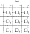
- a memory cell arrangement comprises first lines L1 which run essentially parallel to one another and second lines L2 which also run essentially parallel to one another.
- the first lines L1 run transversely to the second lines L2 (see FIG. 1).
- the memory cell arrangement comprises memory cells S, which are each connected between one of the first lines L1 and one of the second lines L2. By driving one of the first lines L1 and one of the second lines L2 each of the memory cells S can thus be clearly controlled.
- Each of the memory cells comprises six tunnel elements T1, T2, T3, T4, T5, T6, which are connected to one another via tunnel contacts TK.
- the first of the tunnel elements T1 is connected to a connection of one of the first lines L1 via a first tunnel contact TK1.
- the last of the tunnel elements T6 in the row is connected to a storage node SK via a second tunnel contact TK2.
- the storage node SK can be controlled capacitively via a first gate electrode G1.
- the distance between the first gate electrode G1 and the storage node SK is so large that at the operating voltages provided in the memory cell arrangement there is no tunnel transition between the first gate electrode G1 and the storage node SK (see FIG. 2 and FIG. 3).
- the first gate electrode G1 is connected to one of the second lines L2.
- the first gate electrode G1, the storage node SK and the tunnel elements T1, T2, T3, T4, T5, T6 with the tunnel contacts TK1, TK, TK2 located between them form a storage element.
- each of the memory cells comprises a transistor tunnel element T which is connected to a connection of the first line L1 via a first transistor tunnel contact TK3 and which is connected to a connection of the second line L2 via a second transistor tunnel contact TK4.
- the transistor tunnel element T is driven via a second gate electrode G2, which is connected to the storage node SK.
- the distance between the second gate electrode G2 and the transistor tunnel element T is so large that the control takes place capacitively and that a tunnel junction between the second gate electrode G2 and the transistor tunnel element T does not occur at the operating voltages of the memory cell arrangement.
- the transistor tunnel element T, the first transistor tunnel contact TK3, the second transistor tunnel contact TK4 and the second gate electrode G2 form a single electron transistor.
- the tunnel elements T1, T2, T3, T4, T5, T6 are implemented, for example, as conductive islands with, for example, a round cross section on an insulating surface.
- the tunnel elements T1, T6 are formed, for example, from gold, aluminum or titanium with a diameter of, for example, 3 nm.
- the insulating surface on which the memory cell is arranged is, for example, the surface of an SiO 2 layer which is arranged on a silicon substrate.
- the memory cell arrangement can also be arranged on a substrate made of sapphire.
- the distance between adjacent tunnel elements T1, T2, T3, T4, T5, T6 and thus the dimensions of the tunnel contacts TK1, TK, TK2 is, for example, 2 nm.
- the storage node SK and the second gate electrode G2, as well as the first gate electrode G1 and the lines L1 and L2 are implemented as metallic areas on the insulating surface, for example. They are also made of gold, aluminum or titanium.
- the distance between the first gate electrode G1 and the storage node SK is 5 nm, for example.
- the dimensions of the storage node SK are, for example, 3 nm.
- the transistor tunnel element T is also formed as a conductive island, for example made of gold, aluminum or titanium, for example with a round cross section with a diameter of 3 nm.
- the connections to the first line L1 and to the second line L2 are likewise implemented as metallic conductor tracks made of, for example, gold, aluminum and titanium.
- the distance from the transistor tunnel element to the connections to the first line L1 or second line L2 and thus the dimensions of the transistor tunnel contacts TK3, TK4 are 2 nm.
- the distance between the second gate electrode G2 and the transistor tunnel element T is 5 nm.
- the area requirement per memory cell is approximately 500 nm 2 .
- a 1 Tbit memory cell arrangement can thus be implemented on an area of 5 cm 2 .
- the memory cell is produced, for example, by depositing individual metal atoms on an insulating surface using a scanning tunneling microscope or an atomic force microscope.
- an entire metal layer with a thickness of, for example, 3 nm can be structured by lithography, in particular using electron radiation or synchrotron radiation, or by oxidation with a scanning probe microscope.
- the non-conductive gaps between the tunnel elements can be produced both by oxidation of an originally metallic layer and by using lithographic processes and reactive ion etching.
- the tunnel resistance of the tunnel contacts TK1, TK, TK2 is 100 k ⁇ and the associated capacitance is 1 aF.
- the capacitance of the first gate electrode C G is 1 aF.
- the capacitance of the transistor tunnel contacts TK3, TK4 is 0.1 aF in each case.
- the capacitance of the second gate electrode G2 is 0.3 aF.
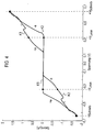
- the memory cell is operated with a read voltage V read of 0.32 volts and a write voltage of 0.64 volts.
- a first characteristic curve K1 and a second characteristic curve K2 are shown in FIG.
- the first characteristic curve K1 applies in the event that the charge state + e is stored in the storage element.
- the second characteristic curve K2 applies in the event that the charge state - e is stored in the storage element. If there is a voltage + V read between the first line L1 and the second line L2 and the charge state + e is stored in the storage element, a current of about 0.8 ⁇ A flows through the transistor. If, on the other hand, the state of charge - e is stored, no current flows through the transistor when a voltage of + V read is applied .
- the write voltage + V write By applying the write voltage + V write , if the charge state + e is stored, the current increases, the charge state passes through zero, which is unstable, and the charge state - e is written into the memory element when the level + V write is reached .
- a voltage level -V write is applied, in which, if the charge state - e was stored, the unstable state is passed through zero and the charge state + e is written into the memory element.
- the read voltage V read is selected such that a distinction can be made between the charge states - e and + e via the current flow, but that the stable charge states + e and - e are not recharged.
Landscapes
- Engineering & Computer Science (AREA)
- Microelectronics & Electronic Packaging (AREA)
- Chemical & Material Sciences (AREA)
- Nanotechnology (AREA)
- Computer Hardware Design (AREA)
- Physics & Mathematics (AREA)
- Mathematical Physics (AREA)
- Theoretical Computer Science (AREA)
- Crystallography & Structural Chemistry (AREA)
- Semiconductor Memories (AREA)
- Static Random-Access Memory (AREA)
- Read Only Memory (AREA)
Abstract
Description
- Speicherzellenanordnungen mit wahlfreiem dynamischem Zugriff, DRAM, werden derzeit hauptsächlich in CMOS-Technologie hergestellt. Sie umfassen Speicherzellen mit jeweils einem Auslesetransistor und einem Kondensator. Auf dem Kondensator wird die zu speichernde Information in Form einer Ladungsmenge gespeichert. Üblicherweise beträgt die Signalladung etwa 50 fC, das heißt sie besteht aus 300000 Elektronen. Die Kapazität des Kondensators in heutigen Speicherzellen beträgt 20 bis 30 fF.
- Mit zunehmender Packungsdichte zukünftiger Speicheranordnungen nimmt die Fläche pro Speicherzelle ab. Dabei wird es immer schwieriger bis schließlich unmöglich auf der für die Speicherzelle zur Verfügung stehenden Fläche einen Kondensator mit der relativ großen Speicherkapazität von 20 bis 30 fF herzustellen. Auch der Auslesetransistor kann nicht beliebig verkleinert werden.
- Im Hinblick auf eine weitere Miniaturisierung sind sogenannte Einzelelektron-Bauelemente vorgeschlagen worden, in denen Schaltvorgänge mit einzelnen Elektronen realisiert werden. Eine Untersuchung über derartige Einzelelektron-Bauelemente ist zum Beispiel aus W. Rösner et al, Microelectronic Engineering, Bd. 27, 1995, Seiten 55 bis 58, bekannt. Einzelelektron-Bauelemente umfassen Tunnelelemente, die über Tunnelkontakte mit benachbarten Anschlüssen verbunden sind. Ladungsübertritte über diese Tunnelkontakte erfolgen sowohl über den quantenmechanischen Tunneleffekt als auch durch einfache thermische Überwindung einer Potentialbarriere, wobei diese Ladungsübertritte hinreichend selten auftreten. Die Tunnelelemente sind zum Beispiel als kleine leitfähige Inseln realisiert, die von einer isolierenden Struktur umgeben sind.
- Wird an die beiden Anschlüsse eine Spannung U angelegt, für die die Bedingung für Coulomb-Blockade erfüllt ist, das heißt für deren Betrag

- Bei Anlegen einer höheren Spannung können Elektronen über einen der Tunnelkontakte auf das Tunnelelement fließen. Diese Einzelelektron-Bauelemente werden so betrieben, daß jeweils ein Übertritt einzelner Elektronen erfolgt.
- Durch Ansteuerung des Tunnelelementes über eine Gateelektrode, die das Tunnelelement kapazitiv beeinflußt, ohne daß es im Betriebsspannungsbereich zu Tunnelübergängen käme, ist ein Stromfluß über das Tunnelelement möglich. Sofern an der Gateelektrode eine geeignete elektrische Ladung wirksam ist, weist das Einzelelektron-Bauelement eine in etwa lineare, durch den Nullpunkt gehende Stromspannungskennlinie auf. Ein derartiges gategesteuertes Einzelelektron-Bauelement wird in der Literatur als Einzelelektron-Transistor bezeichnet.
- In K. Nakazato et al, J. Appl. Phys., Bd. 75, Nr. 10, 1994, Seiten 5123-5134, ist eine Einzelelektron-Speicherzelle vorgeschlagen worden. Diese umfaßt drei sogenannte Multitunnelelemente. Als Multitunnelelement wird eine Reihenschaltung von Tunnelelementen bezeichnet, die jeweils über einen Tunnelkontakt miteinander verbunden sind. Die Multitunnelelemente weisen jeweils eine seitliche Gateelektrode auf, über die ein Strom durch die Multitunnelelemente steuerbar ist. Ein erstes Multitunnelelement und ein zweites Multitunnelelement ist dabei zwischen eine erste Spannungsquelle und Masse in Reihe verschaltet. Die beiden Multitunnelelemente sind über einen Speicherknoten miteinander verbunden. Die seitlichen Gateelektroden der Multitunnelelemente sind mit einer zweiten Spannungsquelle bzw. einer dritten Spannungsquelle verbunden.
- Der Speicherknoten ist über eine Kapazität mit einer vierten Spannungsquelle verbunden. Der Speicherknoten ist über eine weitere Kapazität mit einem dritten Multitunnelelement verbunden, das zwischen eine fünfte Spannungsquelle und Masse geschaltet ist. Das dritte Multitunnelelement wird ebenfalls durch eine seitliche Gateelektrode angesteuert, die mit einer sechsten Spannungsquelle verbunden ist.
- Das dritte Multitunnelelement wirkt als Elektrometer, mit dem auf dem Speicherknoten befindliche Ladung nachgewiesen wird. Messungen, bei denen die seitliche Gateelektrode des zweiten Multitunnelelementes mit einer hohen negativen Spannung beaufschlagt wurde, haben ergeben, daß in dem ersten Multitunnelelement und im Speicherknoten einzelne Elektronen stabil gespeichert werden können, sofern die an das Multitunnelelement angelegte Spannung die Bedingung für Coulomb-Blockade erfüllt. Abhängig von der an die seitliche Gateelektrode angelegten Spannung können in dem aus Speicherknoten und erstem Multitunnelelement gebildeten Speicherelement eine diskrete Anzahl von Elektronen stabil gespeichert werden. Dieses wird damit erklärt, daß die elektrostatische Energie des Speicherelementes für die jeweils entsprechende Anzahl gespeicherter Elektronen einen metastabilen Zustand einnimmt. Zwischen benachbarten, metastabilen Zuständen weist die elektrostatische Energie einen Potentialwall auf, dessen Scheitel höher als der nächste metastabile Zustand ist. Die Höhe der Potentialwälle hängt von der Anzahl der gespeicherten Elektronen und der Anzahl der Tunnelkontakte im Multitunnelelement ab.
- Die Einzelelektron-Speicherzelle ist in Delta-dotiertem GaAs realisiert. Da zum Betrieb der Einzelelektron-Speicherzelle sechs Spannungsquellen erforderlich sind, ist eine Speicherzellenanordnung, die eine Vielzahl derartiger Speicherzellen umfaßt, aufwendig ansteuerbar.
- Der Erfindung liegt daher das Problem zugrunde, eine Einzelelektron-Speicherzellenanordnung anzugeben, die mit einem geringeren Aufwand ansteuerbar ist.
- Dieses Problem wird erfindungsgemäß gelöst durch eine Einzelelektron-Speicherzellenanordnung, die Speicherzellen mit jeweils einem Einzelelektron-Speicherelement und einem Einzelelektron-Transistor umfassen. Jede der Speicherzellen ist zwischen eine erste Leitung und eine zweite Leitung geschaltet. Die Speicherzellenanordnung umfaßt parallel verlaufende erste Leitungen und parallel verlaufende zweite Leitungen, wobei die ersten Leitungen und die zweiten Leitungen quer zueinander verlaufen. Die ersten Leitungen und die zweiten Leitungen sind vergleichbar mit den Wort- und Bitleitungen in derzeitigen DRAM-Anordnungen.
- Da in der erfindungsgemäßen Einzelelektron-Speicherzellenanordnung jede Speicherzelle zwischen eine der ersten Leitungen und eine der zweiten Leitungen geschaltet ist, läßt sich jede der Speicherzellen durch Anlegen entsprechender Spannungspegel an die zugehörige erste Leitung und die zugehörige zweite Leitung einfach ansteuern.
- Das Einzelelektron-Speicherelement umfaßt mindestens ein Tunnelelement, das über einen ersten Tunnelkontakt mit der ersten Leitung und über einen zweiten Tunnelkontakt mit einem Speicherknoten verbunden ist, der über eine erste Gateelektrode kapazitiv ansteuerbar ist. Über die Tunnelkontakte erfolgen Ladungsübertritte sowohl durch quantenmechanischen Tunneleffekt als auch durch hinreichend seltene thermische Überwindung einer Potentialbarriere. Ist der Tunnelwiderstand

- Die Kapazitäten des Speicherelementes und des Einzelelektron-Transistors sind so abgestimmt, daß bei Anliegen einer Lesespannung durch den Einzelelektron-Transistor ein von einer im Speicherelement gespeicherten Ladung abhängiger Strom fließt. Die im Speicherelement gespeicherte Ladung wird dabei nicht verändert. Durch Anlegen einer Schreibspannung, die betragsmäßig größer als die Lesespannung ist, ist dagegen die im Speicherelement gespeicherte Ladung veränderbar.
- Die Erfindung macht sich die Erkenntnis zunutze, daß ein Einzelelektron-Transistor ein empfindliches Elektrometer für eine an der Gateelektrode des Einzelelektron-Transistors wirksame Ladung ist. Die Lesespannung wird so gewählt, daß die Bedingung für Coulomb-Blockade erfüllt ist. Der über den Einzelelektron-Transistor fließende Strom ist abhängig von der auf dem Speicherknoten befindlichen Ladung, da der Speicherknoten mit der zweiten Gateelektrode des Einzelelektron-Transistors verbunden ist. Gleichzeitig wird eine Veränderung der auf dem Speicherknoten gespeicherten Ladung dadurch verhindert, daß die an der ersten Gateelektrode anliegende Lesespannung zu einer Änderung der auf dem Speicherknoten befindlichen elektrischen Ladung nicht ausreicht. Dabei wird ausgenutzt, daß die Anzahl der Elektronen, die stabil in einem Multitunnelelement gespeichert werden können sowohl von der Anzahl der Tunnelkontakte in dem Multitunnelelement als auch von der Gatespannung, mit der das Multitunnelelement angesteuert wird, abhängt.
- Die Kapazitäten des Einzelelektron-Speicherelementes und des Einzelelektron-Transistors werden so aufeinander abgestimmt, daß gleichzeitig bei Anliegen der Lesespannung für den Einzelelektron-Transistor die Bedingung für Coulomb-Blockade erfüllt ist und eine Veränderung des Ladungszustands des Einzelelektron-Speicherelementes nicht möglich ist. Bei der betragsmäßig höheren Schreibspannung wird dagegen eine Veränderung des Ladungszustandes des Speicherknotens bewirkt.
- Zur Ansteuerung einer Speicherzelle zum Lesen der Information wird zwischen die zugehörigen erste Leitung und zweite Leitung ein Spannungspegel entsprechend der Lesespannung angelegt. Die übrigen ersten Leitungen und zweiten Leitungen werden mit demselben Potential wie die ausgewählte erste Leitung verbunden, so daß alle Zellen, die nicht zu der ausgewählten zweiten Leitung gehören, spannungsfrei sind. Zum Einschreiben von Informationen in eine Speicherzelle wird zwischen die zugehörige erste Leitung und zweite Leitung ein Spannungspegel entsprechend der Schreibspannung angelegt. Die übrigen ersten Leitungen und zweiten Leitungen werden so beschaltet, daß über die übrigen Speicherzellen ein geringerer Spannungspegel abfällt, bei dem keine Veränderung der gespeicherten Ladung auftritt. Die übrigen Leitungen können zum Beispiel mit einem Spannungspegel entsprechend der Lesespannung oder der Differenz von Schreib- und Lesespannung beaufschlagt werden.
- Vorzugsweise werden die Kapazitäten des Speicherelementes und des Einzelelektron-Transistors so abgestimmt, daß der Betrag der Lesespannung halb so groß wie der Betrag der Schreibspannung ist. Beim Einschreiben von Information in eine Speicherzelle können in diesem Fall die übrigen ersten Leitungen und die zweiten Leitungen mit der Lesespannung beaufschlagt werden und es fällt über einen Teil der nicht ausgewählten Speicherzellen immer dieselbe Spannung ab. Die übrigen nicht ausgewählten Speicherzellen sind spannungsfrei.
- Vorzugsweise umfaßt das Speicherelement mehrere Tunnelelemente, die untereinander jeweils über Tunnelkontakte als Reihe miteinander verbunden sind. Für die Eigenschaften dieser Tunnelkontakte gilt das in bezug auf den ersten Tunnelkontakt und den zweiten Tunnelkontakt Gesagte. Das erste Tunnelelement ist dabei über den ersten Tunnelkontakt mit der ersten Leitung und das in der Reihe letzte Tunnelelement über den zweiten Tunnelkontakt mit dem Speicherknoten verbunden. Das Vorsehen mehrerer Tunnelkontakte im Speicherelement führt dazu, daß die Anzahl der stabilen Ladungszustände in dem Speicherelement für eine feste Spannung an der ersten Gateelektrode zunimmt.
- Als Tunnelelemente kommen alle Strukturen in Betracht, die einen elektrisch leitfähigen Bereich umfassen und die über eine Isolationsstruktur gegenüber benachbarten elektrisch leitfähigen Bereichen isoliert sind. Über die Isolationsstruktur sind die elektrisch leitfähigen Bereiche durch Tunnelkontakte verbunden. Als Tunnelelemente sind insbesondere Strukturen geeignet, die einen leitfähigen Kern und einen den leitfähigen Kern umgebende isolierende Hülle umfassen. Der Durchmesser des Tunnelelements liegt dabei vorzugsweise zwischen 1 und 10 nm. Die Kapazität der Tunnelelemente ist in diesem Größenbereich so klein, daß die Speicherzellenanordnung im Raumtemperaturbereich funktioniert. Insbesondere sind als Tunnelelemente Metallcluster mit organischen Liganden als isolierende Hülle, wie sie aus DE 42 12 220 A1 bekannt sind, oder Fullerene mit eingeschlossenem Metallkern geeignet.
- Desweiteren sind als Tunnelelemente lithographisch strukturierte dünne Metallschichten geeignet, wobei die Tunnelkontakte durch Oxidation einer solchen Metallschicht und nachfolgender Abscheidung und Strukturierung einer weiteren Metallschicht entstehen.
- Im Rahmen einer molekularen Elektronik sind als Tunnelelemente auch Abschnitte einzelner Moleküle geeignet, die abhängig von ihrer Vorgeschichte unterschiedliche Ladungen tragen können. Der Ladungsübertritt zwischen solchen umladbaren Molekülabschnitten erfolgt entlang chemischer Bindungen.
- Unter der Voraussetzung, daß der Tunnelwiderstand der Tunnelkontakte


- CG Kapazität der ersten Gateelektrode
- C Kapazität eines Tunnelkontaktes im Speicherelement
- n Anzahl der Tunnelkontakte im Speicherelement
- V Spannung an der 1. Gateelektrode
- I Anzahl der im Speicherelement gespeicherten Elektronen
- e Elektronenladung
- Für eine Speicherzelle, die bei Anlegen einer Schreibspannung ±VSchreib die stabilen Zustände + e und - e einnimmt, folgt aus der Bedingung für stabile Ladungszustände

- Die Bedingung, daß der Ladungszustand null Elektronen bei Anliegen der Schreibspannung VSchreib instabil ist, führt zu

- Bei Anliegen der Lesespannung VLese soll insbesondere der Ladungszustand +e stabil sein, also


- CΣt Gesamtkapazität des Transistors.
- Die Gesamtkapazität des Einzelelektron-Transistors ergibt sich als Summe der Kapazitäten der Tunnelkontakte, die den Einzelelektron-Transistor bilden und der Kapazität der zweiten Gateelektrode.
- Diese Bedingungen sind erfüllt für folgende Spannungen und Kapazitäten:

- Die Erfindung ist nicht auf diese Kapazitätswerte beschränkt. Durch Wahl einer anderen Lesespannung VLese, durch Ausnutzung des vollen Bereichs der Ungleichungen, durch Vorgabe anderer und / oder mehr stabiler Ladungszustände bei der Lese- beziehungsweise Schreibspannung oder durch andere Annahmen bei der Ableitung des Stabilitätskriteriums, zum Beispiel daß die Tunnelkontakte unterschiedliche Kapazität aufweisen, lassen sich in analoger Weise andere Kriterien für die Kapazitäten bestimmen.
- Im folgenden wird die Erfindung anhand der Figuren und eines Ausführungsbeispiels näher erläutert.
- Figur 1
- zeigt ein schematisches Schaltbild einer Speicherzellenanordnung.
- Figur 2
- zeigt eine Aufsicht auf eine Speicherzelle.
- Figur 3
- Zeigt das Ersatzschaltbild für die in Figur 2 dargestellte Speicherzelle.
- Figur 4
- zeigt Kennlinien der Speicherzelle.
- Eine Speicherzellenanordnung umfaßt erste Leitungen L1, die im wesentlichen parallel zueinander verlaufen und zweite Leitungen L2, die ebenfalls im wesentlichen parallel zueinander verlaufen. Die ersten Leitungen L1 verlaufen dabei quer zu den zweiten Leitungen L2 (siehe Figur 1).
- Die Speicherzellenanordnung umfaßt Speicherzellen S, die jeweils zwischen einem der ersten Leitungen L1 und eine der zweiten Leitungen L2 geschaltet sind. Durch Ansteuerung einer der ersten Leitungen L1 und einer der zweiten Leitungen L2 läßt sich damit jede der Speicherzellen S eindeutig ansteuern.
- Jede der Speicherzellen umfaßt sechs Tunnelelemente T1, T2, T3, T4, T5, T6, die untereinander über Tunnelkontakte TK miteinander verbunden sind. Das erste der Tunnelelemente T1 ist über einen ersten Tunnelkontakt TK1 mit einem Anschluß einer der ersten Leitungen L1 verbunden. Das in der Reihe letzte der Tunnelelemente T6 ist über einen zweiten Tunnelkontakt TK2 mit einem Speicherknoten SK verbunden. Der Speicherknoten SK ist über eine erste Gateelektrode G1 kapazitiv ansteuerbar. Der Abstand zwischen der ersten Gateelektrode G1 und dem Speicherknoten SK ist so groß, daß bei den in der Speicherzellenanordnung vorgesehenen Betriebsspannungen kein Tunnelübergang zwischen der ersten Gateelektrode G1 und dem Speicherknoten SK erfolgt (siehe Figur 2 und Figur 3). Die erste Gateelektrode G1 ist mit einer der zweiten Leitungen L2 verbunden.
- Die erste Gateelektrode G1, der Speicherknoten SK sowie die Tunnelelemente T1, T2, T3, T4, T5, T6 mit den dazwischen befindlichen Tunnelkontakten TK1, TK, TK2 bilden ein Speicherelement.
- Ferner umfaßt jede der Speicherzellen ein Transistortunnelelement T, das über einen ersten Transistortunnelkontakt TK3 mit einem Anschluß der ersten Leitung L1 verbunden ist und das über einen zweiten Transistortunnelkontakt TK4 mit einem Anschluß der zweiten Leitung L2 verbunden ist. Das Transistortunnelelement T wird über eine zweite Gateelektrode G2, die mit dem Speicherknoten SK verbunden ist, angesteuert. Der Abstand zwischen der zweiten Gateelektrode G2 und dem Transistortunnelelement T ist so groß, daß die Ansteuerung kapazitiv erfolgt und daß bei den Betriebsspannungen der Speicherzellenanordnung ein Tunnelübergang zwischen der zweiten Gateelektrode G2 und dem Transistortunnelelement T unterbleibt. Das Transistortunnelelement T, der erste Transistortunnelkontakt TK3, der zweite Transistortunnelkontakt TK4 und die zweite Gateelektrode G2 bilden einen Einzelelektron-Transistor.
- Die Tunnelelemente T1, T2, T3, T4, T5, T6 werden zum Beispiel als leitfähige Inseln mit zum Beispiel rundem Querschnitt auf einer isolierenden Oberfläche realisiert. Die Tunnelelemente T1, T6 werden zum Beispiel aus Gold, Aluminium oder Titan mit einem Durchmesser von zum Beispiel 3 nm gebildet. Die isolierende Oberflache, auf der die Speicherzelle angeordnet ist, ist zum Beispiel die Oberfläche einer SiO2-Schicht, die auf einem Siliziumsubstrat angeordnet ist. Die Speicherzellenanordnung kann ferner auf einem Substrat aus Saphir angeordnet werden.
- Der Abstand benachbarter Tunnelelemente T1, T2, T3, T4, T5, T6 und damit die Abmessungen der Tunnelkontakte TK1, TK, TK2 beträgt zum Beispiel 2 nm. Der Speicherknoten SK und die zweite Gateelektrode G2, sowie die erste Gateelektrode G1 und die Leitungen L1 und L2 werden zum Beispiel als metallische Gebiete auf der isolierenden Oberfläche realisiert. Sie werden ebenfalls aus Gold, Aluminium oder Titan gebildet. Der Abstand zwischen der ersten Gateelektrode G1 und dem Speicherknoten SK beträgt zum Beispiel 5 nm.
- Die Abmessungen des Speicherknotens SK betragen zum Beispiel 3 nm.
- Das Transistortunnelelement T ist ebenfalls als leitfähige Insel zum Beispiel aus Gold, Aluminium oder Titan mit zum Beispiel rundem Querschnitt mit einem Durchmesser von 3 nm gebildet. Die Anschlüsse zur ersten Leitung L1 und zur zweiten Leitung L2 sind ebenfalls als metallische Leiterbahnen aus zum Beispiel Gold, Aluminium und Titan realisiert. Der Abstand des Transistortunnelelementes zu den Anschlüssen zur ersten Leitung L1 bzw. zweiten Leitung L2 und damit die Abmessungen der Transistortunnelkontakte TK3, TK4 betragen 2 nm. Der Abstand zwischen der zweiten Gateelektrode G2 und dem Transistortunnelelement T beträgt 5 nm.
- Der Flächenbedarf pro Speicherzelle beträgt etwa 500 nm2. Eine 1Tbit-Speicherzellenanordnung ist damit auf einer Fläche von 5 cm2 realisierbar.
- Die Speicherzelle wird zum Beispiel durch Abscheidung einzelner Metallatome auf einer isolierenden Oberfläche mithilfe eines Rastertunnelmikroskops oder eines Atomkraftmikroskops hergestellt.
- Alternativ kann eine ganzflächige Metallschicht einer Dicke von zum Beispiel 3 nm durch Lithgraphie, insbesondere unter Verwendung von Elektronenstrahlung oder Synchrotronstrahlung, oder durch Oxidation mit einem Rastersondenmikroskop strukturiert werden.
- Die nicht leitenden Zwischenräume zwischen den Tunnelelementen können sowohl durch Oxidation einer ursprünglich metallischen Schicht als auch unter Verwendung lithographischer Verfahren und reaktivem Ionenätzen hergestellt werden.
- Beispielsweise beträgt der Tunnelwiderstand der Tunnelkontakte TK1, TK, TK2 jeweils 100 kΩ und die zugehörige Kapazität beträgt jeweils 1 aF. Die Kapazität der ersten Gateelektrode CG beträgt 1 aF. Die Kapazität der Transistortunnelkontakte TK3, TK4 beträgt jeweils 0,1 aF. Die Kapazität der zweiten Gateelektrode G2 beträgt 0,3 aF. Damit beträgt die Gesamtkapazität des Einzelelektron-Speichertransistors

- Die Speicherzelle wird mit einer Lesespannung VLese von 0,32 Volt und einer Schreibspannung von 0,64 Volt betrieben.
- Anhand der in Figur 4 dargestellten Kennlinien der Speicherzelle wird im folgenden der Betrieb der Speicherzelle erläutert. In Figur 4 sind eine erste Kennlinie K1 und eine zweite Kennlinie K2 dargestellt. Die erste Kennlinie K1 gilt für den Fall, daß in dem Speicherelement der Ladungszustand + e gespeichert ist. Die zweite Kennlinie K2 gilt für den Fall, daß in dem Speicherelement der Ladungszustand - e gespeichert ist. Liegt zwischen der ersten Leitung L1 und der zweiten Leitung L2 eine Spannung +VLese an, und ist in dem Speicherelement der Ladungszustand + e gespeichert, so fließt über den Transistor ein Strom von etwa 0,8 µA. Ist dagegen der Ladungszustand - e gespeichert, so fließt bei Anlegen einer Spannung von +VLese kein Strom über den Transistor.
- Bei Anlegen einer Spannung von -VLese fließt kein Strom über den Transistor, falls der Ladungszustand + e gespeichert ist und ein Strom von etwa - 0,8 µA, falls der Ladungszustand - e gespeichert ist.
- Durch Anlegen der Schreibspannung +VSchreib steigt, falls der Ladungszustand + e gespeichert ist, der Strom an, es wird der Ladungszustand Null durchlaufen, der instabil ist und es wird bei Erreichen des Pegels +VSchreib der Ladungszustand - e in das Speicherelement eingeschrieben. Zum Einschreiben des Ladungszustands + e wird ein Spannungspegel -VSchreib angelegt, bei dem, falls der Ladungszustand - e gespeichert war, der instabile Zustand Null durchlaufen wird und der Ladungszustand + e in das Speicherelement eingeschrieben wird. Die Lesespannung VLese ist so gewählt, daß zwar über den Stromfluß deutlich zwischen den Ladungszuständen - e und + e unterschieden werden kann, daß jedoch eine Umladung der stabilen Ladungszustände + e und - e unterbleibt.
Claims (7)
- Einzelelektron-Speicherzellenanordnung,- bei der parallel verlaufende erste Leitungen und parallel verlaufende zweite Leitungen, die quer zu den ersten Leitungen verlaufen, vorgesehen sind,- bei der Speicherzellen vorgesehen sind, die jeweils zwischen eine der ersten Leitungen und eine der zweiten Leitungen geschaltet sind,- bei der die Speicherzellen jeweils ein Einzelelektron-Speicherelement und einen Einzelelektron-Transistor umfassen,- bei der das Einzelelektron-Speicherelement mindestens ein Tunnelelement umfaßt, das über einen ersten Tunnelkontakt mit der ersten Leitung und über einen zweiten Tunnelkontakt mit einem Speicherknoten verbunden ist, der über eine erste Gateelektrode kapazitiv ansteuerbar ist,- bei der die erste Gateelektrode mit der zweiten Leitung verbunden ist,- bei der der Einzelelektron-Transistor über einen ersten Anschluß mit der ersten Leitung und über einen zweiten Anschluß mit der zweiten Leitung verbunden ist und über eine zweite Gateelektrode kapazitiv ansteuerbar ist,- bei der die zweite Gateelektrode mit dem Speicherknoten verbunden ist,- bei der die Kapazitäten des Speicherelementes und des Einzelelektron-Transistors so abgestimmt sind, daß bei Anliegen einer Lesespannung, die betragsmäßig geringer als eine Schreibspannung ist, zwischen der ersten Leitung und der zweiten Leitung durch den Einzelelektron-Transistor ein von einer im Speicherelement gespeicherten Ladung abhängiger Strom fließt, ohne die im Speicherelement gespeicherte Ladung zu verändern und daß bei der Anliegen der Schreibspannung zwischen der ersten Leitung und der zweiten Leitung die im Speicherelement gespeicherte Ladung veränderbar ist.
- Einzelelektron-Speicherzellenanordnung nach Anspruch 1, bei der die Kapazitäten des Speicherelementes und des Einzelelektron-Transistors so abgestimmt sind, daß der Betrag der Lesespannung halb so groß wie der Betrag der Schreibspannung ist.
- Einzelelektron-Speicherzellenanordnung nach Anspruch 1 oder 2,
bei der das Speicherelement mehrere Tunnelelemente umfaßt, die untereinander jeweils über Tunnelkontakte als Reihe verbunden sind, wobei das erste Tunnelelement über den ersten Tunnelkontakt mit der ersten Leitung und das in der Reihe letzte Tunnelelement über den zweiten Tunnelkontakt mit dem Speicherknoten verbunden sind. - Einzelelektron-Speicherzellenanordnung nach Anspruch 3, bei der die Tunnelelemente jeweils im wesentlichen dieselbe Kapazität aufweisen.
- Einzelelektron-Speicherzellenanordnung nach Anspruch 4, bei der für die Kapazitäten in dem Speicherelement und in dem Einzelelektron-Transistor folgende Bedingungen gelten:
 C: Kapazität eines Tunnelkontaktes im SpeicherelementCG: Kapazität der ersten GateelektrodeCΣt: Gesamtkapazität des Einzelelektron-Transistorsn: Anzahl der Tunnelkontakte im SpeicherelementVLese: LesespannungVSchreib: Schreibspannung
 - Einzelelektron-Speicherzellenanordnung nach einem der Ansprüche 1 bis 5,- bei der die Tunnelelemente jeweils einen leitfähigen Kern und eine den leitfähigen Kern umgebende isolierende Hülle umfassen,- bei der der leitfähige Kern und die isolierende Hülle gemeinsam einen Durchmesser zwischen 0,1 um und 10 um aufweisen.
- Einzelelektron-Speicherzellenanordnung nach einem der Ansprüche 1 bis 5,
bei der die Tunnelelemente jeweils Teilbereiche einer ursprünglich ganzflächigen metallischen Schicht sowie nicht leitende Zwischenräume umfassen.
Applications Claiming Priority (2)
| Application Number | Priority Date | Filing Date | Title |
|---|---|---|---|
| DE19621994 | 1996-05-31 | ||
| DE19621994A DE19621994C1 (de) | 1996-05-31 | 1996-05-31 | Einzelelektron-Speicherzellenanordnung |
Publications (3)
| Publication Number | Publication Date |
|---|---|
| EP0810609A2 true EP0810609A2 (de) | 1997-12-03 |
| EP0810609A3 EP0810609A3 (de) | 1999-08-11 |
| EP0810609B1 EP0810609B1 (de) | 2002-03-06 |
Family
ID=7795864
Family Applications (1)
| Application Number | Title | Priority Date | Filing Date |
|---|---|---|---|
| EP97107314A Expired - Lifetime EP0810609B1 (de) | 1996-05-31 | 1997-05-02 | Einzelelektron-Speicherzellenanordnung |
Country Status (7)
| Country | Link |
|---|---|
| US (1) | US5844834A (de) |
| EP (1) | EP0810609B1 (de) |
| JP (1) | JP4057675B2 (de) |
| KR (1) | KR100435924B1 (de) |
| AT (1) | ATE214194T1 (de) |
| DE (2) | DE19621994C1 (de) |
| TW (1) | TW382707B (de) |
Cited By (1)
| Publication number | Priority date | Publication date | Assignee | Title |
|---|---|---|---|---|
| KR20010042194A (ko) * | 1998-05-05 | 2001-05-25 | 인피니언 테크놀로지스 아게 | 단일 전자 소자들을 포함하는 회로 장치 및 작동 방법 |
Families Citing this family (13)
| Publication number | Priority date | Publication date | Assignee | Title |
|---|---|---|---|---|
| EP0881691B1 (de) * | 1997-05-30 | 2004-09-01 | Matsushita Electric Industrial Co., Ltd. | Anordnung mit Quanten-Schachteln |
| KR100325689B1 (ko) | 1999-12-01 | 2002-02-25 | 오길록 | 전자-홀 결합을 이용한 단전자 메모리 소자 |
| US6483125B1 (en) | 2001-07-13 | 2002-11-19 | North Carolina State University | Single electron transistors in which the thickness of an insulating layer defines spacing between electrodes |
| US6653653B2 (en) | 2001-07-13 | 2003-11-25 | Quantum Logic Devices, Inc. | Single-electron transistors and fabrication methods in which a projecting feature defines spacing between electrodes |
| US6673717B1 (en) | 2002-06-26 | 2004-01-06 | Quantum Logic Devices, Inc. | Methods for fabricating nanopores for single-electron devices |
| US7135697B2 (en) * | 2004-02-25 | 2006-11-14 | Wisconsin Alumni Research Foundation | Spin readout and initialization in semiconductor quantum dots |
| US7602069B2 (en) * | 2004-03-31 | 2009-10-13 | Universität Duisburg-Essen | Micro electronic component with electrically accessible metallic clusters |
| EP1748501B1 (de) * | 2005-07-26 | 2007-10-17 | Universität Duisburg-Essen | Mikroelektronisches Bauelement |
| KR100673408B1 (ko) * | 2005-02-07 | 2007-01-24 | 최중범 | 싱글 일렉트론 트랜지스터를 채용하는 메모리 셀 및 그메모리 장치 |
| US20090066853A1 (en) * | 2007-09-10 | 2009-03-12 | Sony Corporation Sony Electronics Inc. | Remote control with recessed keypad |
| US20120235968A1 (en) * | 2011-03-15 | 2012-09-20 | Qualcomm Mems Technologies, Inc. | Method and apparatus for line time reduction |
| US9558820B2 (en) | 2013-10-29 | 2017-01-31 | Hewlett Packard Enterprise Development Lp | Resistive crosspoint memory array sensing |
| WO2019060999A1 (en) * | 2017-09-28 | 2019-04-04 | Quantum Silicon Inc. | INITIATION AND MONITORING THE EVOLUTION OF INDIVIDUAL ELECTRONS IN ATOM DEFINED STRUCTURES |
Family Cites Families (2)
| Publication number | Priority date | Publication date | Assignee | Title |
|---|---|---|---|---|
| US5357460A (en) * | 1991-05-28 | 1994-10-18 | Sharp Kabushiki Kaisha | Semiconductor memory device having two transistors and at least one ferroelectric film capacitor |
| DE4212220C3 (de) * | 1992-04-09 | 2000-05-04 | Guenter Schmid | Verwendung einer Anordnung aus Clustermolekülen als mikroelektronisches Bauelement |
-
1996
- 1996-05-31 DE DE19621994A patent/DE19621994C1/de not_active Expired - Fee Related
-
1997
- 1997-05-02 AT AT97107314T patent/ATE214194T1/de not_active IP Right Cessation
- 1997-05-02 DE DE59706533T patent/DE59706533D1/de not_active Expired - Fee Related
- 1997-05-02 EP EP97107314A patent/EP0810609B1/de not_active Expired - Lifetime
- 1997-05-27 TW TW086107163A patent/TW382707B/zh not_active IP Right Cessation
- 1997-05-28 JP JP15308497A patent/JP4057675B2/ja not_active Expired - Fee Related
- 1997-05-29 KR KR1019970021474A patent/KR100435924B1/ko not_active Expired - Fee Related
- 1997-06-02 US US08/867,114 patent/US5844834A/en not_active Expired - Lifetime
Non-Patent Citations (4)
| Title |
|---|
| KANUO YANO ET AL: "ROOM-TEMPERATURE SINGLE-ELECTRON MEMORY" IEEE TRANSACTIONS ON ELECTRON DEVICES, Bd. 41, Nr. 9, 1. September 1994, Seiten 1628-1638, XP000466806 * |
| KAZUO YANO ET AL: "A ROOM-TEMPERATURE SINGLE-ELECTRON MEMORY DEVICE USING FINE-GRAIN POLYCRYSTALLINE SILICON" PROCEEDINGS OF THE INTERNATIONAL ELECTRON DEVICES MEETING, WASHINGTON, DEC. 5 - 8, 1993,5. Dezember 1993, Seiten 541-544, XP000481675 INSTITUTE OF ELECTRICAL AND ELECTRONICS ENGINEERS * |
| NAKAZATO K ET AL: "SINGLE-ELECTRON MEMORY" ELECTRONICS LETTERS, Bd. 29, Nr. 4, 18. Februar 1993, Seite 384/385 XP000346076 * |
| NAKAZATO K ET AL: "SINGLE-ELECTRON MEMORY" JOURNAL OF APPLIED PHYSICS, Bd. 75, Nr. 10, PART 01, 15. Mai 1994, Seiten 5123-5134, XP000456680 * |
Cited By (1)
| Publication number | Priority date | Publication date | Assignee | Title |
|---|---|---|---|---|
| KR20010042194A (ko) * | 1998-05-05 | 2001-05-25 | 인피니언 테크놀로지스 아게 | 단일 전자 소자들을 포함하는 회로 장치 및 작동 방법 |
Also Published As
| Publication number | Publication date |
|---|---|
| JPH1098160A (ja) | 1998-04-14 |
| KR970076815A (ko) | 1997-12-12 |
| TW382707B (en) | 2000-02-21 |
| EP0810609A3 (de) | 1999-08-11 |
| ATE214194T1 (de) | 2002-03-15 |
| US5844834A (en) | 1998-12-01 |
| JP4057675B2 (ja) | 2008-03-05 |
| DE59706533D1 (de) | 2002-04-11 |
| EP0810609B1 (de) | 2002-03-06 |
| KR100435924B1 (ko) | 2004-07-16 |
| DE19621994C1 (de) | 1997-06-12 |
Similar Documents
| Publication | Publication Date | Title |
|---|---|---|
| DE3203516C2 (de) | ||
| DE69803781T2 (de) | Festwertspeicher und festwertspeicheranordnung | |
| EP0810609B1 (de) | Einzelelektron-Speicherzellenanordnung | |
| WO1998053504A1 (de) | Ein-elektron-speicherbauelement | |
| CH670914A5 (de) | ||
| EP1170799A2 (de) | Elektronisches Bauelement und Verfahren zum Herstellen eines elektronischen Bauelements | |
| DE19705001A1 (de) | Dynamischer Speicher mit wahlfreiem Zugriff ohne Kondensator und Verfahren zum Herstellen eines derartigen Speichers | |
| DE4208694A1 (de) | Halbleiter-speicherbauelement | |
| DE2628383A1 (de) | Monolithischer halbleiterspeicher fuer wahlfreien zugriff mit abfuehlschaltungen | |
| DE10058047A1 (de) | Integrierter Speicher mit einer Anordnung von nicht-flüchtigen Speicherzellen und Verfahren zur Herstellung und zum Betrieb des integrierten Speichers | |
| DE3002492C2 (de) | ||
| DE69324823T2 (de) | Speicheranordnung | |
| DE2532594A1 (de) | Halbleiterspeicher | |
| DE19950362C1 (de) | DRAM-Zellenanordnung, Verfahren zu deren Betrieb und Verfahren zu deren Herstellung | |
| DE10207980C1 (de) | Floating-Gate-Speicherzelle, Floating-Gate-Speicheranordnung, Schaltkreis-Anordnung und Verfahren zum Herstellen einer Floating-Gate-Speicherzelle | |
| EP0664569B1 (de) | Mikroelektronisches Bauelement | |
| DE2431079A1 (de) | Dynamischer halbleiterspeicher mit zwei-tranistor-speicherelementen | |
| EP1126471B1 (de) | Verfahren zum Auslesen oder Speichern eines Zustandes aus einem oder in einen ferroelektrischen Transistor einer Speicherzelle und Speichermatrix | |
| DE19929308C1 (de) | Verfahren zur Herstellung einer ferroelektrischen Speicheranordnung | |
| WO2004051763A2 (de) | Verfahren zum herstellen einer speicherzelle, speicherzelle und speicherzellen-anordnung | |
| DE4327653C2 (de) | Nichtflüchtige Halbleiterspeichervorrichtung mit verbessertem Koppelverhältnis und Verfahren zur Herstellung einer solchen | |
| EP0001986A2 (de) | Hochintegrierte Speichermatrix und Verfahren zu ihrer Herstellung | |
| EP1078461B1 (de) | Schaltungsanordnung mit einzelelektron-bauelementen und verfahren zu deren betrieb | |
| DE69618044T2 (de) | Speicherzelle | |
| DE4026409A1 (de) | Elektrisch programmier- und loeschbarer halbleiterspeicher und verfahren zu seinem betrieb |
Legal Events
| Date | Code | Title | Description |
|---|---|---|---|
| PUAI | Public reference made under article 153(3) epc to a published international application that has entered the european phase |
Free format text: ORIGINAL CODE: 0009012 |
|
| AK | Designated contracting states |
Kind code of ref document: A2 Designated state(s): AT DE FR GB IE IT NL |
|
| PUAL | Search report despatched |
Free format text: ORIGINAL CODE: 0009013 |
|
| AK | Designated contracting states |
Kind code of ref document: A3 Designated state(s): AT DE FR GB IE IT NL |
|
| RIC1 | Information provided on ipc code assigned before grant |
Free format text: 6G 11C 11/34 A, 6G 11C 11/40 B |
|
| 17P | Request for examination filed |
Effective date: 19990903 |
|
| GRAG | Despatch of communication of intention to grant |
Free format text: ORIGINAL CODE: EPIDOS AGRA |
|
| GRAG | Despatch of communication of intention to grant |
Free format text: ORIGINAL CODE: EPIDOS AGRA |
|
| GRAH | Despatch of communication of intention to grant a patent |
Free format text: ORIGINAL CODE: EPIDOS IGRA |
|
| 17Q | First examination report despatched |
Effective date: 20010803 |
|
| RAP1 | Party data changed (applicant data changed or rights of an application transferred) |
Owner name: INFINEON TECHNOLOGIES AG |
|
| GRAH | Despatch of communication of intention to grant a patent |
Free format text: ORIGINAL CODE: EPIDOS IGRA |
|
| REG | Reference to a national code |
Ref country code: GB Ref legal event code: IF02 |
|
| GRAA | (expected) grant |
Free format text: ORIGINAL CODE: 0009210 |
|
| AK | Designated contracting states |
Kind code of ref document: B1 Designated state(s): AT DE FR GB IE IT NL |
|
| PG25 | Lapsed in a contracting state [announced via postgrant information from national office to epo] |
Ref country code: NL Free format text: LAPSE BECAUSE OF FAILURE TO SUBMIT A TRANSLATION OF THE DESCRIPTION OR TO PAY THE FEE WITHIN THE PRESCRIBED TIME-LIMIT Effective date: 20020306 Ref country code: IT Free format text: LAPSE BECAUSE OF FAILURE TO SUBMIT A TRANSLATION OF THE DESCRIPTION OR TO PAY THE FEE WITHIN THE PRESCRIBED TIME-LIMIT;WARNING: LAPSES OF ITALIAN PATENTS WITH EFFECTIVE DATE BEFORE 2007 MAY HAVE OCCURRED AT ANY TIME BEFORE 2007. THE CORRECT EFFECTIVE DATE MAY BE DIFFERENT FROM THE ONE RECORDED. Effective date: 20020306 Ref country code: IE Free format text: LAPSE BECAUSE OF FAILURE TO SUBMIT A TRANSLATION OF THE DESCRIPTION OR TO PAY THE FEE WITHIN THE PRESCRIBED TIME-LIMIT Effective date: 20020306 Ref country code: GB Free format text: LAPSE BECAUSE OF FAILURE TO SUBMIT A TRANSLATION OF THE DESCRIPTION OR TO PAY THE FEE WITHIN THE PRESCRIBED TIME-LIMIT Effective date: 20020306 Ref country code: FR Free format text: LAPSE BECAUSE OF FAILURE TO SUBMIT A TRANSLATION OF THE DESCRIPTION OR TO PAY THE FEE WITHIN THE PRESCRIBED TIME-LIMIT Effective date: 20020306 |
|
| REF | Corresponds to: |
Ref document number: 214194 Country of ref document: AT Date of ref document: 20020315 Kind code of ref document: T |
|
| REF | Corresponds to: |
Ref document number: 59706533 Country of ref document: DE Date of ref document: 20020411 |
|
| PG25 | Lapsed in a contracting state [announced via postgrant information from national office to epo] |
Ref country code: AT Free format text: LAPSE BECAUSE OF NON-PAYMENT OF DUE FEES Effective date: 20020502 |
|
| NLV1 | Nl: lapsed or annulled due to failure to fulfill the requirements of art. 29p and 29m of the patents act | ||
| GBV | Gb: ep patent (uk) treated as always having been void in accordance with gb section 77(7)/1977 [no translation filed] |
Effective date: 20020306 |
|
| REG | Reference to a national code |
Ref country code: IE Ref legal event code: FD4D |
|
| PG25 | Lapsed in a contracting state [announced via postgrant information from national office to epo] |
Ref country code: DE Free format text: LAPSE BECAUSE OF NON-PAYMENT OF DUE FEES Effective date: 20021203 |
|
| EN | Fr: translation not filed | ||
| PLBE | No opposition filed within time limit |
Free format text: ORIGINAL CODE: 0009261 |
|
| STAA | Information on the status of an ep patent application or granted ep patent |
Free format text: STATUS: NO OPPOSITION FILED WITHIN TIME LIMIT |
|
| 26N | No opposition filed |
Effective date: 20021209 |
|
| REG | Reference to a national code |
Ref country code: HK Ref legal event code: WD Ref document number: 1003522 Country of ref document: HK |