EP0810652B1 - Halbleiteranordnung - Google Patents
Halbleiteranordnung Download PDFInfo
- Publication number
- EP0810652B1 EP0810652B1 EP97111478A EP97111478A EP0810652B1 EP 0810652 B1 EP0810652 B1 EP 0810652B1 EP 97111478 A EP97111478 A EP 97111478A EP 97111478 A EP97111478 A EP 97111478A EP 0810652 B1 EP0810652 B1 EP 0810652B1
- Authority
- EP
- European Patent Office
- Prior art keywords
- single crystal
- layer
- porous
- substrate
- source
- Prior art date
- Legal status (The legal status is an assumption and is not a legal conclusion. Google has not performed a legal analysis and makes no representation as to the accuracy of the status listed.)
- Expired - Lifetime
Links
Images
Classifications
-
- H—ELECTRICITY
- H10—SEMICONDUCTOR DEVICES; ELECTRIC SOLID-STATE DEVICES NOT OTHERWISE PROVIDED FOR
- H10D—INORGANIC ELECTRIC SEMICONDUCTOR DEVICES
- H10D30/00—Field-effect transistors [FET]
- H10D30/01—Manufacture or treatment
- H10D30/021—Manufacture or treatment of FETs having insulated gates [IGFET]
- H10D30/031—Manufacture or treatment of FETs having insulated gates [IGFET] of thin-film transistors [TFT]
- H10D30/0321—Manufacture or treatment of FETs having insulated gates [IGFET] of thin-film transistors [TFT] comprising silicon, e.g. amorphous silicon or polysilicon
- H10D30/0323—Manufacture or treatment of FETs having insulated gates [IGFET] of thin-film transistors [TFT] comprising silicon, e.g. amorphous silicon or polysilicon comprising monocrystalline silicon
-
- H—ELECTRICITY
- H10—SEMICONDUCTOR DEVICES; ELECTRIC SOLID-STATE DEVICES NOT OTHERWISE PROVIDED FOR
- H10D—INORGANIC ELECTRIC SEMICONDUCTOR DEVICES
- H10D30/00—Field-effect transistors [FET]
- H10D30/60—Insulated-gate field-effect transistors [IGFET]
- H10D30/67—Thin-film transistors [TFT]
- H10D30/6729—Thin-film transistors [TFT] characterised by the electrodes
- H10D30/673—Thin-film transistors [TFT] characterised by the electrodes characterised by the shapes, relative sizes or dispositions of the gate electrodes
- H10D30/6733—Multi-gate TFTs
- H10D30/6734—Multi-gate TFTs having gate electrodes arranged on both top and bottom sides of the channel, e.g. dual-gate TFTs
-
- H—ELECTRICITY
- H10—SEMICONDUCTOR DEVICES; ELECTRIC SOLID-STATE DEVICES NOT OTHERWISE PROVIDED FOR
- H10D—INORGANIC ELECTRIC SEMICONDUCTOR DEVICES
- H10D30/00—Field-effect transistors [FET]
- H10D30/60—Insulated-gate field-effect transistors [IGFET]
- H10D30/67—Thin-film transistors [TFT]
- H10D30/674—Thin-film transistors [TFT] characterised by the active materials
- H10D30/6741—Group IV materials, e.g. germanium or silicon carbide
-
- H—ELECTRICITY
- H10—SEMICONDUCTOR DEVICES; ELECTRIC SOLID-STATE DEVICES NOT OTHERWISE PROVIDED FOR
- H10D—INORGANIC ELECTRIC SEMICONDUCTOR DEVICES
- H10D30/00—Field-effect transistors [FET]
- H10D30/60—Insulated-gate field-effect transistors [IGFET]
- H10D30/67—Thin-film transistors [TFT]
- H10D30/674—Thin-film transistors [TFT] characterised by the active materials
- H10D30/6741—Group IV materials, e.g. germanium or silicon carbide
- H10D30/6743—Silicon
- H10D30/6744—Monocrystalline silicon
-
- H—ELECTRICITY
- H10—SEMICONDUCTOR DEVICES; ELECTRIC SOLID-STATE DEVICES NOT OTHERWISE PROVIDED FOR
- H10D—INORGANIC ELECTRIC SEMICONDUCTOR DEVICES
- H10D84/00—Integrated devices formed in or on semiconductor substrates that comprise only semiconducting layers, e.g. on Si wafers or on GaAs-on-Si wafers
- H10D84/01—Manufacture or treatment
- H10D84/0123—Integrating together multiple components covered by H10D12/00 or H10D30/00, e.g. integrating multiple IGBTs
- H10D84/0126—Integrating together multiple components covered by H10D12/00 or H10D30/00, e.g. integrating multiple IGBTs the components including insulated gates, e.g. IGFETs
- H10D84/0165—Integrating together multiple components covered by H10D12/00 or H10D30/00, e.g. integrating multiple IGBTs the components including insulated gates, e.g. IGFETs the components including complementary IGFETs, e.g. CMOS devices
-
- H—ELECTRICITY
- H10—SEMICONDUCTOR DEVICES; ELECTRIC SOLID-STATE DEVICES NOT OTHERWISE PROVIDED FOR
- H10D—INORGANIC ELECTRIC SEMICONDUCTOR DEVICES
- H10D84/00—Integrated devices formed in or on semiconductor substrates that comprise only semiconducting layers, e.g. on Si wafers or on GaAs-on-Si wafers
- H10D84/01—Manufacture or treatment
- H10D84/02—Manufacture or treatment characterised by using material-based technologies
- H10D84/03—Manufacture or treatment characterised by using material-based technologies using Group IV technology, e.g. silicon technology or silicon-carbide [SiC] technology
- H10D84/038—Manufacture or treatment characterised by using material-based technologies using Group IV technology, e.g. silicon technology or silicon-carbide [SiC] technology using silicon technology, e.g. SiGe
-
- H—ELECTRICITY
- H10—SEMICONDUCTOR DEVICES; ELECTRIC SOLID-STATE DEVICES NOT OTHERWISE PROVIDED FOR
- H10D—INORGANIC ELECTRIC SEMICONDUCTOR DEVICES
- H10D86/00—Integrated devices formed in or on insulating or conducting substrates, e.g. formed in silicon-on-insulator [SOI] substrates or on stainless steel or glass substrates
- H10D86/201—Integrated devices formed in or on insulating or conducting substrates, e.g. formed in silicon-on-insulator [SOI] substrates or on stainless steel or glass substrates the substrates comprising an insulating layer on a semiconductor body, e.g. SOI
-
- H—ELECTRICITY
- H10—SEMICONDUCTOR DEVICES; ELECTRIC SOLID-STATE DEVICES NOT OTHERWISE PROVIDED FOR
- H10D—INORGANIC ELECTRIC SEMICONDUCTOR DEVICES
- H10D88/00—Three-dimensional [3D] integrated devices
-
- H—ELECTRICITY
- H10—SEMICONDUCTOR DEVICES; ELECTRIC SOLID-STATE DEVICES NOT OTHERWISE PROVIDED FOR
- H10P—GENERIC PROCESSES OR APPARATUS FOR THE MANUFACTURE OR TREATMENT OF DEVICES COVERED BY CLASS H10
- H10P90/00—Preparation of wafers not covered by a single main group of this subclass, e.g. wafer reinforcement
- H10P90/19—Preparing inhomogeneous wafers
- H10P90/1904—Preparing vertically inhomogeneous wafers
- H10P90/1906—Preparing SOI wafers
-
- H—ELECTRICITY
- H10—SEMICONDUCTOR DEVICES; ELECTRIC SOLID-STATE DEVICES NOT OTHERWISE PROVIDED FOR
- H10W—GENERIC PACKAGES, INTERCONNECTIONS, CONNECTORS OR OTHER CONSTRUCTIONAL DETAILS OF DEVICES COVERED BY CLASS H10
- H10W10/00—Isolation regions in semiconductor bodies between components of integrated devices
- H10W10/01—Manufacture or treatment
- H10W10/061—Manufacture or treatment using SOI processes together with lateral isolation, e.g. combinations of SOI and shallow trench isolations
-
- H—ELECTRICITY
- H10—SEMICONDUCTOR DEVICES; ELECTRIC SOLID-STATE DEVICES NOT OTHERWISE PROVIDED FOR
- H10W—GENERIC PACKAGES, INTERCONNECTIONS, CONNECTORS OR OTHER CONSTRUCTIONAL DETAILS OF DEVICES COVERED BY CLASS H10
- H10W10/00—Isolation regions in semiconductor bodies between components of integrated devices
- H10W10/10—Isolation regions comprising dielectric materials
- H10W10/181—Semiconductor-on-insulator [SOI] isolation regions, e.g. buried oxide regions of SOI wafers
-
- H—ELECTRICITY
- H10—SEMICONDUCTOR DEVICES; ELECTRIC SOLID-STATE DEVICES NOT OTHERWISE PROVIDED FOR
- H10P—GENERIC PROCESSES OR APPARATUS FOR THE MANUFACTURE OR TREATMENT OF DEVICES COVERED BY CLASS H10
- H10P90/00—Preparation of wafers not covered by a single main group of this subclass, e.g. wafer reinforcement
- H10P90/19—Preparing inhomogeneous wafers
- H10P90/1904—Preparing vertically inhomogeneous wafers
- H10P90/1906—Preparing SOI wafers
- H10P90/1914—Preparing SOI wafers using bonding
-
- H—ELECTRICITY
- H10—SEMICONDUCTOR DEVICES; ELECTRIC SOLID-STATE DEVICES NOT OTHERWISE PROVIDED FOR
- H10W—GENERIC PACKAGES, INTERCONNECTIONS, CONNECTORS OR OTHER CONSTRUCTIONAL DETAILS OF DEVICES COVERED BY CLASS H10
- H10W10/00—Isolation regions in semiconductor bodies between components of integrated devices
- H10W10/01—Manufacture or treatment
- H10W10/011—Manufacture or treatment of isolation regions comprising dielectric materials
- H10W10/012—Manufacture or treatment of isolation regions comprising dielectric materials using local oxidation of silicon [LOCOS]
-
- H—ELECTRICITY
- H10—SEMICONDUCTOR DEVICES; ELECTRIC SOLID-STATE DEVICES NOT OTHERWISE PROVIDED FOR
- H10W—GENERIC PACKAGES, INTERCONNECTIONS, CONNECTORS OR OTHER CONSTRUCTIONAL DETAILS OF DEVICES COVERED BY CLASS H10
- H10W10/00—Isolation regions in semiconductor bodies between components of integrated devices
- H10W10/10—Isolation regions comprising dielectric materials
- H10W10/13—Isolation regions comprising dielectric materials formed using local oxidation of silicon [LOCOS], e.g. sealed interface localised oxidation [SILO] or side-wall mask isolation [SWAMI]
Definitions
- the present invention relates to a semiconductor device, more particularly a semiconductor device including an insulated gate transistor.
- semiconductor devices effective in improving a performance level there is a transistor of the type that a semiconductor thin film on an insulating layer is used as an active region.
- SOI Silicon-On-Insulator
- the SOI technique is practiced by, for instance, a method of condensing and irradiating an energy beam, such as an electron ray and a laser beam, onto an amorphous or polycrystal Si layer and growing a single crystal layer on SiO 2 by recrystallization through melt, or a method of forming an SiO 2 layer in a single crystal Si substrate by ion implantation of oxygen (called a SIMOX (Separation by Ion Implanted Oxygen) process).
- an energy beam such as an electron ray and a laser beam
- Such a structure that a semiconductor thin film is formed on an insulating layer by using the SOI technique to suppress a short channel effect is proposed in, for instance, "Manufacture of very thin-film MOSFET/SIMOX with gate length of 0.15 ⁇ m and its characteristics", 1991 Autumn Congress of Japanese Electron Information Communication Society, SC-9-3.
- This paper describes that thinning the Si layer is effective in suppression of a short channel region effect and thinning a buried oxide film below the channel region is effective in suppression of a short channel effect upon the threshold voltage. It is also described that thinning the buried oxide film raises a problem of increasing parasitic capacity associated with source and drain regions.
- a double gate MOS has recently been also developed which includes a second gate on the side opposite to a semiconductor layer, where source and drain regions are formed, and a usual gate with insulating layer therebetween.
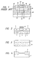
- Fig. 1 shows one example of such a double gate MOS.
- Denoted by reference numeral 61 is a substrate, 62 to 62" are insulating layers, 63 is a second gate, 64 is a source region, and 65 is a drain region.
- a source electrode 67 and a drain electrode 68 are connected to the source region 64 and the drain region 65, respectively.
- a portion 66 sandwiched between the source region 64 and the drain region 65 is a channel portion, and 69 denotes a first gate for controlling the channel portion.
- the double gate MOS have advantages of improving a short channel effect and increasing a current driving force.
- document JP-A-56 029 369 discloses an IGFET having an insulating layer, wherein a portion thereof under the source and drain region is thick and a portion under the channel between said regions is thin. Further, a thin gate insulating layer is deposited on these regions.
- document JP-A-61 125 163 discloses a semiconductor device in which an oxide film for isolating elements is formed in an element isolation region, and a lower layer MOS-transistor consisting of a gate oxide film, a gate electrode and source-drain regions is shaped in an element forming region. Also, an inter-layer insulating film is deposited on the whole surface and the surface is flattened.
- document EP-A-0 063 915 discloses a metal insulator semiconductor (MIS) transistor which is built on an insulating layer being arranged with a thin portion under the channel region of the MIS-transistor and a thick portion under the remainder of the device.
- MIS metal insulator semiconductor
- a single crystal Si layer is formed by using a porous Si substrate which is obtained by changing a single crystal Si substrate into porous Si.
- a transmission electron-microscopic observation shows that the porous Si substrate has micro-pores of about 60 ⁇ m (600 ⁇ ) in mean diameter.. Also, while the porous Si substrate has density less than a half that of the single crystal Si substrate, single crystallinity is still maintained and a single crystal Si layer can be formed on the porous layer through epitaxial growth. At a temperature not lower than 100°C, however, internal micro-pores are rearranged to impair a characteristic of enhanced etching.
- a low-temperature method such as a molecular beam epitaxial growth process, plasma CVD process, thermal CVD process, optical CVD process, bias-sputtering process, crystal growth process, etc. is suitable for epitaxial growth of the Si layer.
- a single crystal Si substrate is prepared and then changed into porous Si by an anodization process using an HF solution. While single crystal Si has density of 2.33 g/cm 3 , the density of porous Si can be varied in the range of 0.6 to 1.1 g/cm 3 when the content of the HF solution is varied between 20 and 50 weight %.
- the porous Si layer tends to be easily formed on a P-type Si substrate from the following reason.
- Porous Si was discovered in the course of studies of electrolytic grinding of semiconductors. In a dissolving reaction of Si during anodization, holes are required for an anodic reaction of Si in an HF solution and the anodic reaction is expressed as follows; Si + 2HF + (2 - n)e + ⁇ SiF 2 + 2H + + ne - SiF 2 + 2HF ⁇ SiF 4 + H 2 SiF 4 + 2HF ⁇ H 2 SiF 6 or Si + 4HF + (4 - ⁇ )e + ⁇ SiF 4 + 4H + + ⁇ e - SiF 4 + 2HF ⁇ H 2 SiF 6 where e + and e - respectively represent a hole and an electron, and n and ⁇ each represent the number of holes necessary for one Si atom to dissolve. It is reported that porous Si is formed on condition of n > 2 or ⁇ > 4.
- a porous layer has a great number of voids formed therein and its density is as small as half or below that of the non-porous structure.
- the porous structure has a much increased surface area per unit volume and, therefore, a porous layer exhibits a much greater chemical etching rate than an ordinary single crystal layer.
- a single crystal Si thin film is formed through epitaxial growth on the porous Si substrate formed by the above anodization.
- a thickness of the single crystal Si thin film is preferably not larger than 50 ⁇ m, more preferably not larger than 20 ⁇ m.
- the oxide film on the single crystal Si surface is bonded to the substrate.
- the surface of a single crystal Si substrate, newly prepared is oxidized and then bonded to the single crystal Si layer on the porous Si substrate.
- the reason why the oxide film is provided between the substrate and the single crystal Si layer is below.
- the interface level produced by the underlying interface of an Si active layer is lower for the glass interface than for the oxide film interface and, therefore, characteristics of an electronic device can be improved remarkably.
- both the members adhere closely to each other by van der Waals' forces to such an extent that they cannot be easily separated.
- both the members are completely bonded to each other by heat treatment under a nitrogen atmosphere at temperature in the range of 200 to 900°C, preferably 600 to 900°C.
- an Si 3 N 4 layer is deposited as an etching prevention layer all over the two substrates bonded to each other, followed by removing only the Si 3 N 4 layer which is located on the surface of the porous Si substrate.
- Apiezon wax may be used instead of the Si 3 N 4 layer.
- the porous Si substrate is totally removed by etching or any other suitable means, thereby providing a semiconductor substrate with the thin film single crystal Si layer.
- an etchant which has no etching action upon crystal Si but enables selective etching of porous Si alone, are hydrofluoric acid, buffered hydrofluoric acid such as ammonium fluoride (NH 4 F) or hydrogen fluoride (HF), a mixture of hydrofluoric acid or buffered hydrofluoric acid added with an aqueous solution of hydrogen peroxide, a mixture of hydrofluoric acid or buffered hydrofluoric acid added with alcohol, and a mixture of hydrofluoric acid or buffered hydrofluoric acid added with an aqueous solution of hydrogen peroxide and alcohol.
- Etching is made by immersing the bonded substrates in any of those solutions for etching.
- An etching rate depends on the content and the temperature of hydrofluoric acid, buffered hydrofluoric acid, and the aqueous solution of hydrogen peroxide.
- the oxidation of Si can be accelerated so as to realize a greater reaction speed than the case where hydrogen peroxide is not added.
- the reaction speed is controllable by varying the content of the aqueous solution of hydrogen peroxide.
- voids of etching reaction product gases can be instantaneously removed from the etched surface without requiring agitation of the etchant, so that porous Si can be uniformly and efficiently etched.
- the HF content in the buffered hydrofluoric acid is set to be preferably in the range of 1 to 95 weight % for the etchant, more preferably 1 to 85 weight %, most preferably 1 to 70 weight %.
- the NH 4 F content in the buffered hydrofluoric acid is set to be preferably in the range of 1 to 95 weight % for the etchant, more preferably 5 to 90 weight %, most preferably 5 to 80 weight %.
- the HF content is set to be preferably in the range of 1 to 95 weight % for the etchant, more preferably 5 to 90 weight %, most preferably 5 to 80 weight %.
- the H 2 O 2 content is set to be preferably in the range of 1 to 95 weight % for the etchant, more preferably 5 to 90 weight %, most preferably 10 to 80 weight %, and also in the range where the effect of addition of hydrogen peroxide is maintained.
- the alcohol content is set to be preferably not larger than 80 weight % for the etchant, more preferably not larger than 60 weight %, most preferably not larger than 40 weight %, and also in the range where the effect of addition of alcohol is maintained.
- the temperature is set to be preferably in the range of 0 to 100°C, more preferably 5 to 80°C, most preferably 5 to 60°C.
- Alcohol used in the present process can be any suitable alcohol, such as ethylalcohol and isopropyl alcohol, which does not cause any problem from the view point of practical production process and with which the effect of addition of alcohol is expected.
- an insulating film By making the single crystal Si thin film, obtained through the above process, subjected to ion implantation of O 2 or bonded to another Si wafer having an insulating film thereon, an insulating film can be obtained which has two single crystal Si thin films on both sides.
- the Si film thickness prior to the implantation is preferably in the range of 1 to 5 ⁇ m depending on purpose.
- O 2 ions are implanted with density of 5 x 10 17 to 5 x 10 18 cm -2 at acceleration energy of 200 keV, followed by heat treatment for several hours at temperature in the range of 1100 to 1200°C.
- the insulating film is formed to be 50 to 1000 ⁇ m (500 to 10000 ⁇ ) thick and, after bonding, Si on the outermost surface can be thinned to be 200 ⁇ m (2000 ⁇ ) to several ⁇ m thick by grinding.
- the former ion implantation process is preferably used in the present invention.
- a manufacture method for a semiconductor device is as follows. Thick selective oxide films are formed just below those regions on a first single crystal substrate which become source and drain regions, the first single crystal substrate is flattened, and then an oxide film is formed on the flattened. substrate surface, thereby fabricating a first substrate in which thick oxide films are formed in those regions going to locate just below the source and drain regions, and a thin oxide film is formed in that region going to locate just below a channel region.
- a non-porous single crystal Si layer with good crystallinity is formed on a second single crystal Si substrate which has been changed into porous Si and has a high etching rate, or an insulating layer is further formed on the non-porous single crystal Si layer, thereby fabricating a second substrate.
- the second single crystal Si substrate which has been changed into porous Si is removed by treatment including at least wet chemical etching.
- a thin single crystal Si layer with good crystallinity and uniform film thickness is formed on the bonded insulating layer by a simple process.
- the source and drain regions are formed on the thick selective oxide films.
- a gate electrode on the above single crystal semiconductor layer, forming a selective oxide film in the region around the gate electrode, and flattening the formed selective oxide film and an oxide film on the gate electrode, a wiring pattern or the like can be formed on the flattened oxide film surface.
- a laminated semiconductor device which has an insulated gate field effect transistor in the underlying layer.
- a first gate is preferably formed to have a film thickness not smaller than 50 ⁇ m (500 ⁇ ), more preferably not smaller than 200 ⁇ m (2000 ⁇ ). If the film thickness is smaller than 50 ⁇ m (500 ⁇ ), there would be a fear of undesirable increase in the gate resistance value.
- a film thickness of the first gate is preferably in the range of 50 to 1000 ⁇ m (500 to 10000 ⁇ ), more preferably in the range of 200 to 600 ⁇ m (2000 to 6000 ⁇ ). If the film thickness is not larger than 50 ⁇ m (500 ⁇ ), there would be a feat of undesirable increase in the gate resistance value. On the other hand, if it is too thick, there would arise difficulties in making pixel portions completely transparent.
- the area ratio between first and second gates is not particularly limited. Taking into account characteristics as a double gate device, however, when the first and second gates are used in one-to-one relation, the area ratio of second to first gate is preferably in the range of 1/1 to 10/1. If the first gate is too small or the second gate is too large, there would cause undesirable problems in connection and alignment between the first and second gates, etc., which would complicate the manufacture process and lead to the increased production cost. Further, it is also possible to make one second gate shared by all NMOS transistors and the other second gate shared by all PMOS transistors for controlling two groups of NMOS and PMOS transistors at the same time per group. In this case, the first and second gates are not connected and controlled independently of each other, and no particular limitations are imposed on the area ratio of second to first electrode.
- Fig. 2 is a sectional view for explaining the construction of an N-type MOS transistor according to an explanatory example.
- Fig. 2 denoted by reference numeral 1 is a single crystal Si substrate, 2, 3, 4 are respectively a source region, a channel region and a drain region, 5, 6, 7 are oxide films just below the source region 2, the channel region 3 and the drain region 4, and 8 is a gate electrode.
- the oxide films 5, 7 are selective oxide films made flattened and are formed to have a larger thickness than the oxide film 6.
- parasitic capacity associated with the source and drain regions i.e., parasitic capacity between the substrate and the source region and between the substrate and the drain region
- the oxide film 6 is formed to be thin, a short channel effect can also be suppressed.
- LOCOS Local Oxidation of Silicon
- etch bulk Si and then bury insulating layers of SiON or the like in place.
- the manufacture method for the N-type MOS transistor having the above-mentioned structure comprises the steps of forming a single crystal Si layer on the flattened oxide films which are thick just below only the source and drain regions, and forming a MOS transistor on the single crystal Si layer.
- the method is practiced on the basis of an SOI technique adapted to form the single crystal Si layer on the flattened insulator surface.
- the N-type MOS transistor having the above-mentioned structure may be manufactured by using any of existing SOI techniques, for instance, a method of condensing and irradiating an energy beam such as a laser beam and growing a single crystal layer on SiO 2 by recrystallization through melt, the single crystal Si layer with uniform layer thickness and good crystallinity can be formed on the insulator surface by using the above-explained manufacture method with bonding.
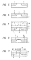
- Figs. 3 to 9 are a series of views showing successive steps for manufacture of the N-type MOS transistor according to this example.
- a non-porous single crystal Si layer 9 is formed through epitaxial growth on the surface of the porous Si substrate.
- a thickness of the single crystal Si layer 9 was set to 0.1 ⁇ m in one experimental example.
- the epitaxial growth is performed by any of such usual methods as a thermal CVD process, reduced-pressure CVD process, plasma CVD process, molecular beam epitaxial process, and sputtering process.
- the selective oxide films 5, 7 being as thick as about 1 ⁇ m are formed on the surface of the single crystal Si substrate in those regions which are to locate just below the source and drain regions.
- the selective oxide films 5, 7 can be formed by patterning an Si 3 N 4 film on the surface of the single crystal. Si substrate in the region which are to locate just below the channel region with an oxide film interposed therebetween, and making it subjected to wet oxidation at 1000°C. Then, as shown in Figs. 5 and 6, the Si 3 N 4 film is removed and SOG (Spin On Glass) is coated on the surface, followed by flattening through reflow. After the flattening, SiO 2 is etched to form the flattened selective oxide films 5, 7. Subsequently, the surface is oxidized to form the oxide film 6 as thin as 20 ⁇ m (200 ⁇ ).
- the single crystal Si substrate 1 having the selective oxide films 5, 7 and the oxide film 6 and the porous Si substrate 10 having the non-porous single crystal Si layer 9 are brought into close contact after cleaning, and then fixedly bonded to each other by being heated under an atmosphere of oxygen, nitrogen, hydrogen, rare gas or the like.
- an oxide film may be formed on the single crystal Si layer 9.
- a certain interface level is possibly produced when fabricating a thin film device through the interface, but such an interface level can be reduced by forming the oxide film on the single crystal Si layer 9.
- the higher the temperature of the heat treatment the stronger is bonding strength at the interface. This is attributable to that at the temperature not lower than about 200°C, both atoms of hydrogen and oxygen having been bonded to each other through the hydrogen bond are removed by dehydration in the form of H 2 O and the condensed silanol bond (Si-O-Si) is left to be formed.
- the bonding strength does not yet reach the maximum level, and it is maximized when those voids are dispersed and vanished thoroughly.
- the bonding strength is saturated in that state and will no longer be intensified even by further increasing the temperature of the heat treatment.
- the temperature at which the bonding strength is saturated is about 1000°C. Therefore, the temperature of the heat treatment was set to about 1000°C in one experimental example.
- the porous Si substrate 10 is etched away by using an etchant below.
- An etchant which can selectively etch the porous Si substrate 10 alone without etching single crystal Si is given by a hydrofluoric acid-base etchant such as hydrofluoric acid and buffered hydrofluoric acid.
- a hydrofluoric acid-base etchant such as hydrofluoric acid and buffered hydrofluoric acid.
- the oxidation of Si can be accelerated so as to realize a greater reaction speed than the case where hydrogen peroxide is not added. Additionally, the reaction speed is controllable by varying the content of the aqueous solution of hydrogen peroxide.
- the porous Si substrate 10 was subjected to selective etching using a mixture solution of 49% hydrofluoric acid, alcohol and a 30% aqueous solution of hydrogen peroxide (10 : 6 : 50) without agitating the etchant.
- the porous Si subtrate 10 was selectively etched and removed completely.
- the single crystal Si layer formed on the oxide film in that way had a uniform layer thickness.
- the gate electrode 8 is formed through a gate insulating film. Then, impurity ions are implanted by using the gate electrode 8 as a mask and annealed to form the source and drain regions 2, 4.
- the gate electrode 8 can be formed on the oxide film 6 with high accuracy by detecting the edges of the selective oxide films 5, 7 by an He-Ne laser from above and forming the gate electrode 8 with the detected edges being as reference. Alternatively, apart from the selective oxide films 5, 7, other selective oxide regions may be formed to serve as alignment marks.
- the N-type MOS transistor shown in Fig. 2 is manufactured.
- a short channel effect can be suppressed by reducing the thickness of the single crystal Si layer and the thickness of the oxide film below the channel region.
- the semiconductor device of the present invention has superior performance and high reliability because it is more simply manufactured than conventional and is free from a fear of reduction in characteristics caused by connection wiring leads.
- a liquid crystal display in which the present semiconductor device can be employed in a peripheral driver circuit it is possible not only to cut down the production cost, but also to drive the'display at a higher power supply voltage than conventional and to increase the degree of freedom in voltage setting, making studies for higher image quality easily made from the viewpoint of circuit arrangement. For instance, a voltage margin necessary for obtaining display with finer gradations is enlarged and, therefore, an allowable maximum value of parasitic capacity in the pixel section is also increased.
- the timings in driving of circuits and so forth required for the higher image quality can be combined in various manners.
- the present semiconductor device has essential conditions for realizing a finer, high-quality display in future. Furthermore, the liquid crystal display in which the present semiconductor device may be employed in a peripheral driver circuit makes it possible, in addition to cut down of the production cost, to speed up the driver circuit and improve its driving characteristics by utilizing the peripheral driver circuit with superior characteristics.
Landscapes
- Thin Film Transistor (AREA)
Claims (1)
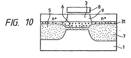
- Halbleitervorrichtung mit einem Transistor mit isolierter Gateelektrode, bei dem Source- und Drainbereiche (2, 4) in einer Einkristallhalbleiterschicht (9) bereitgestellt sind, die auf einer isolierenden Schicht (31) mit Rückflusseigenschaften ausgebildet ist, wobei ein Kanalbereich zwischen dem Source- und dem Drainbereich angeordnet ist, wobei
ein dickes LOCOS-Oxid (5, 7) in einem Substrat (1) genau unter dem Source- und Drainbereich dicker als ein dünnes Nicht-LOCOS-Oxid (6) genau unter dem Kanalbereich (3) ausgebildet ist; und
eine Gateelektrode (8) über dem Kanalbereich (3) ausgebildet ist; wobei
die isolierende Schicht (31) eine kleinere Dicke genau unter dem Source- und dem Drainbereich und eine größere Dicke genau unter dem Kanalbereich aufweist; und
der Niveauunterschied zwischen der isolierenden Schicht (31), dem dicken LOCOS-Oxid (5, 7) und dem dünnen Nicht-LOCOS-Oxid (6) so angeordnet ist, dass die Schnittstelle zwischen der isolierenden Schicht (31) und der Einkristallhalbleiterschicht (9) im wesentlichen flach ausgebildet ist.
Applications Claiming Priority (7)
| Application Number | Priority Date | Filing Date | Title |
|---|---|---|---|
| JP04035729A JP3114894B2 (ja) | 1992-01-28 | 1992-01-28 | 絶縁ゲート型電界効果トランジスタの製造方法、半導体装置の製造方法及び絶縁ゲート型電界効果トランジスタ |
| JP35729/92 | 1992-01-28 | ||
| JP3572992 | 1992-01-28 | ||
| JP4049492 | 1992-01-31 | ||
| JP40494/92 | 1992-01-31 | ||
| JP4049492A JPH05218326A (ja) | 1992-01-31 | 1992-01-31 | 半導体装置及び液晶表示装置 |
| EP93101168A EP0553775B1 (de) | 1992-01-28 | 1993-01-27 | Verfahren zur Herstellung einer Halbleiteranordnung |
Related Parent Applications (2)
| Application Number | Title | Priority Date | Filing Date |
|---|---|---|---|
| EP93101168A Division EP0553775B1 (de) | 1992-01-28 | 1993-01-27 | Verfahren zur Herstellung einer Halbleiteranordnung |
| EP93101168.8 Division | 1993-01-27 |
Publications (3)
| Publication Number | Publication Date |
|---|---|
| EP0810652A2 EP0810652A2 (de) | 1997-12-03 |
| EP0810652A3 EP0810652A3 (de) | 1998-05-20 |
| EP0810652B1 true EP0810652B1 (de) | 2003-05-07 |
Family
ID=26374720
Family Applications (2)
| Application Number | Title | Priority Date | Filing Date |
|---|---|---|---|
| EP97111478A Expired - Lifetime EP0810652B1 (de) | 1992-01-28 | 1993-01-27 | Halbleiteranordnung |
| EP93101168A Expired - Lifetime EP0553775B1 (de) | 1992-01-28 | 1993-01-27 | Verfahren zur Herstellung einer Halbleiteranordnung |
Family Applications After (1)
| Application Number | Title | Priority Date | Filing Date |
|---|---|---|---|
| EP93101168A Expired - Lifetime EP0553775B1 (de) | 1992-01-28 | 1993-01-27 | Verfahren zur Herstellung einer Halbleiteranordnung |
Country Status (3)
| Country | Link |
|---|---|
| US (1) | US6096582A (de) |
| EP (2) | EP0810652B1 (de) |
| DE (2) | DE69317800T2 (de) |
Families Citing this family (36)
| Publication number | Priority date | Publication date | Assignee | Title |
|---|---|---|---|---|
| JPH06314790A (ja) * | 1993-04-23 | 1994-11-08 | Internatl Business Mach Corp <Ibm> | 半導体デバイス及び半導体デバイス製造方法 |
| US7081938B1 (en) | 1993-12-03 | 2006-07-25 | Semiconductor Energy Laboratory Co., Ltd. | Electro-optical device and method for manufacturing the same |
| US6747627B1 (en) | 1994-04-22 | 2004-06-08 | Semiconductor Energy Laboratory Co., Ltd. | Redundancy shift register circuit for driver circuit in active matrix type liquid crystal display device |
| JP3402400B2 (ja) | 1994-04-22 | 2003-05-06 | 株式会社半導体エネルギー研究所 | 半導体集積回路の作製方法 |
| JP3253808B2 (ja) * | 1994-07-07 | 2002-02-04 | 株式会社半導体エネルギー研究所 | 半導体装置およびその作製方法 |
| US5726720A (en) * | 1995-03-06 | 1998-03-10 | Canon Kabushiki Kaisha | Liquid crystal display apparatus in which an insulating layer between the source and substrate is thicker than the insulating layer between the drain and substrate |
| TW335503B (en) | 1996-02-23 | 1998-07-01 | Semiconductor Energy Lab Kk | Semiconductor thin film and manufacturing method and semiconductor device and its manufacturing method |
| TW374196B (en) * | 1996-02-23 | 1999-11-11 | Semiconductor Energy Lab Co Ltd | Semiconductor thin film and method for manufacturing the same and semiconductor device and method for manufacturing the same |
| EP0844661A1 (de) * | 1996-11-20 | 1998-05-27 | STMicroelectronics S.r.l. | Silicium Gate CMOS-Transistore und Verfahren zu ihrer Herstellung |
| KR100238234B1 (ko) * | 1997-03-20 | 2000-01-15 | 윤종용 | 반도체소자용 인-시튜 세정장치 및 그를 이용한 반도체 소자의 세정방법 |
| US6686623B2 (en) | 1997-11-18 | 2004-02-03 | Semiconductor Energy Laboratory Co., Ltd. | Nonvolatile memory and electronic apparatus |
| JP2000012864A (ja) | 1998-06-22 | 2000-01-14 | Semiconductor Energy Lab Co Ltd | 半導体装置の作製方法 |
| US6271101B1 (en) | 1998-07-29 | 2001-08-07 | Semiconductor Energy Laboratory Co., Ltd. | Process for production of SOI substrate and process for production of semiconductor device |
| JP4476390B2 (ja) | 1998-09-04 | 2010-06-09 | 株式会社半導体エネルギー研究所 | 半導体装置の作製方法 |
| WO2000016153A1 (en) * | 1998-09-10 | 2000-03-23 | Seiko Epson Corporation | Substrate for liquid crystal panel, liquid crystal panel, electronic apparatus comprising the panel, and method for manufacturing substrate for liquid crystal panel |
| US6677613B1 (en) * | 1999-03-03 | 2004-01-13 | Semiconductor Energy Laboratory Co., Ltd. | Semiconductor device and method of fabricating the same |
| US6876145B1 (en) * | 1999-09-30 | 2005-04-05 | Semiconductor Energy Laboratory Co., Ltd. | Organic electroluminescent display device |
| US6261876B1 (en) * | 1999-11-04 | 2001-07-17 | International Business Machines Corporation | Planar mixed SOI-bulk substrate for microelectronic applications |
| US6613643B1 (en) | 2000-01-28 | 2003-09-02 | Advanced Micro Devices, Inc. | Structure, and a method of realizing, for efficient heat removal on SOI |
| JP3425603B2 (ja) * | 2000-01-28 | 2003-07-14 | 独立行政法人産業技術総合研究所 | 電界効果トランジスタの製造方法 |
| US6399427B1 (en) * | 2000-02-24 | 2002-06-04 | Advanced Micro Devices, Inc. | Formation of ultra-thin active device area on semiconductor on insulator (SOI) substrate |
| US7101772B2 (en) * | 2000-12-30 | 2006-09-05 | Texas Instruments Incorporated | Means for forming SOI |
| US6759282B2 (en) * | 2001-06-12 | 2004-07-06 | International Business Machines Corporation | Method and structure for buried circuits and devices |
| US6737332B1 (en) * | 2002-03-28 | 2004-05-18 | Advanced Micro Devices, Inc. | Semiconductor device formed over a multiple thickness buried oxide layer, and methods of making same |
| US7611928B2 (en) | 2002-04-16 | 2009-11-03 | Infineon Technologies Ag | Method for producing a substrate |
| DE50312772D1 (de) * | 2002-04-16 | 2010-07-15 | Infineon Technologies Ag | Substrat und verfahren zum herstellen eines substrats |
| US7078773B2 (en) * | 2002-12-23 | 2006-07-18 | International Business Machines Corporation | Nitride-encapsulated FET (NNCFET) |
| FR2860919B1 (fr) * | 2003-10-09 | 2009-09-11 | St Microelectronics Sa | Structures et procedes de fabrication de regions semiconductrices sur isolant |
| JP4420196B2 (ja) * | 2003-12-12 | 2010-02-24 | 三菱電機株式会社 | 誘電体分離型半導体装置およびその製造方法 |
| US7935958B2 (en) * | 2004-10-22 | 2011-05-03 | Semiconductor Energy Laboratory Co., Ltd. | Semiconductor device |
| DE102005027369A1 (de) * | 2005-06-14 | 2006-12-28 | Atmel Germany Gmbh | Integrierter Schaltkreis und Verfahren zur Herstellung eines integrierten Schaltkreises |
| US8049253B2 (en) | 2007-07-11 | 2011-11-01 | Semiconductor Energy Laboratory Co., Ltd. | Semiconductor device and method for manufacturing the same |
| KR101259727B1 (ko) | 2008-10-24 | 2013-04-30 | 가부시키가이샤 한도오따이 에네루기 켄큐쇼 | 반도체 장치 |
| US8859337B2 (en) * | 2009-12-15 | 2014-10-14 | Soitec | Thermal matching in semiconductor devices using heat distribution structures |
| EP2757580A1 (de) * | 2013-01-22 | 2014-07-23 | Nxp B.V. | Bipolar-CMOS-DMOS-Prozesse |
| US9570437B2 (en) | 2014-01-09 | 2017-02-14 | Nxp B.V. | Semiconductor die, integrated circuits and driver circuits, and methods of maufacturing the same |
Family Cites Families (10)
| Publication number | Priority date | Publication date | Assignee | Title |
|---|---|---|---|---|
| JPS5620370A (en) * | 1979-07-28 | 1981-02-25 | Oki Electric Ind Co Ltd | Answer system distributing-charging system |
| JPS5629369A (en) * | 1979-08-17 | 1981-03-24 | Nippon Telegr & Teleph Corp <Ntt> | Insulated gate type field effect transistor |
| JPS57177559A (en) * | 1981-04-24 | 1982-11-01 | Fujitsu Ltd | Semiconductor device and manufacture thereof |
| JPS61125163A (ja) * | 1984-11-22 | 1986-06-12 | Agency Of Ind Science & Technol | 3次元半導体装置 |
| US4829018A (en) * | 1986-06-27 | 1989-05-09 | Wahlstrom Sven E | Multilevel integrated circuits employing fused oxide layers |
| JPH0824162B2 (ja) * | 1989-07-10 | 1996-03-06 | 日本電装株式会社 | 半導体装置およびその製造方法 |
| JP2617798B2 (ja) * | 1989-09-22 | 1997-06-04 | 三菱電機株式会社 | 積層型半導体装置およびその製造方法 |
| US5750000A (en) * | 1990-08-03 | 1998-05-12 | Canon Kabushiki Kaisha | Semiconductor member, and process for preparing same and semiconductor device formed by use of same |
| CA2069038C (en) * | 1991-05-22 | 1997-08-12 | Kiyofumi Sakaguchi | Method for preparing semiconductor member |
| WO1993026041A1 (en) * | 1992-06-17 | 1993-12-23 | Harris Corporation | Bonded wafer processing |
-
1993
- 1993-01-27 EP EP97111478A patent/EP0810652B1/de not_active Expired - Lifetime
- 1993-01-27 DE DE69317800T patent/DE69317800T2/de not_active Expired - Fee Related
- 1993-01-27 DE DE69332960T patent/DE69332960T2/de not_active Expired - Fee Related
- 1993-01-27 EP EP93101168A patent/EP0553775B1/de not_active Expired - Lifetime
-
1997
- 1997-07-23 US US08/898,992 patent/US6096582A/en not_active Expired - Fee Related
Also Published As
| Publication number | Publication date |
|---|---|
| DE69332960D1 (de) | 2003-06-12 |
| DE69317800D1 (de) | 1998-05-14 |
| EP0810652A2 (de) | 1997-12-03 |
| EP0553775B1 (de) | 1998-04-08 |
| EP0810652A3 (de) | 1998-05-20 |
| DE69317800T2 (de) | 1998-09-03 |
| US6096582A (en) | 2000-08-01 |
| HK1004843A1 (en) | 1998-12-11 |
| EP0553775A1 (de) | 1993-08-04 |
| DE69332960T2 (de) | 2004-05-13 |
Similar Documents
| Publication | Publication Date | Title |
|---|---|---|
| EP0810652B1 (de) | Halbleiteranordnung | |
| JP3191061B2 (ja) | 半導体装置及び液晶表示装置 | |
| US20020168802A1 (en) | SiGe/SOI CMOS and method of making the same | |
| US20070075317A1 (en) | Semiconductor device and semiconductor device manufacturing method | |
| US7018882B2 (en) | Method to form local “silicon-on-nothing” or “silicon-on-insulator” wafers with tensile-strained silicon | |
| WO2002103760A2 (en) | Method of selective removal of sige alloys | |
| JP2014179661A (ja) | 半導体装置 | |
| JPH05303116A (ja) | 半導体装置 | |
| JPH05243579A (ja) | 半導体装置 | |
| EP0553774A1 (de) | Halbleiteranordnung und Verfahren zu seiner Herstellung | |
| US6642536B1 (en) | Hybrid silicon on insulator/bulk strained silicon technology | |
| US6169000B1 (en) | Process for the production of semiconductor substrate having silicon-on-insulating structure and process for the production of semiconductor device | |
| US7316943B2 (en) | Method for manufacturing semiconductor apparatus having drain/source on insulator | |
| US5827772A (en) | Fabrication process for thin film transistor | |
| JP3171673B2 (ja) | 薄膜トランジスタ及びその製造方法 | |
| JP3278944B2 (ja) | Soi型半導体装置およびその製造方法 | |
| JPS6227744B2 (de) | ||
| US6350659B1 (en) | Process of making semiconductor device having regions of insulating material formed in a semiconductor substrate | |
| HK1004843B (en) | Semiconductor device and manufacture method of same | |
| JP3114894B2 (ja) | 絶縁ゲート型電界効果トランジスタの製造方法、半導体装置の製造方法及び絶縁ゲート型電界効果トランジスタ | |
| JP2002299590A (ja) | 半導体基板の製造方法及び半導体装置の製造方法 | |
| JPH05218326A (ja) | 半導体装置及び液晶表示装置 | |
| JPH05218434A (ja) | 半導体装置及び液晶表示装置 | |
| JPH098308A (ja) | 半導体素子のトランジスター及びその製造方法 | |
| JP2920937B2 (ja) | Mis型半導体装置の製造方法 |
Legal Events
| Date | Code | Title | Description |
|---|---|---|---|
| PUAI | Public reference made under article 153(3) epc to a published international application that has entered the european phase |
Free format text: ORIGINAL CODE: 0009012 |
|
| AC | Divisional application: reference to earlier application |
Ref document number: 553775 Country of ref document: EP |
|
| AK | Designated contracting states |
Kind code of ref document: A2 Designated state(s): DE FR GB |
|
| PUAL | Search report despatched |
Free format text: ORIGINAL CODE: 0009013 |
|
| AK | Designated contracting states |
Kind code of ref document: A3 Designated state(s): DE FR GB |
|
| 17P | Request for examination filed |
Effective date: 19981009 |
|
| 17Q | First examination report despatched |
Effective date: 20010323 |
|
| RTI1 | Title (correction) |
Free format text: SEMICONDUCTOR DEVICE |
|
| GRAH | Despatch of communication of intention to grant a patent |
Free format text: ORIGINAL CODE: EPIDOS IGRA |
|
| GRAH | Despatch of communication of intention to grant a patent |
Free format text: ORIGINAL CODE: EPIDOS IGRA |
|
| GRAA | (expected) grant |
Free format text: ORIGINAL CODE: 0009210 |
|
| AC | Divisional application: reference to earlier application |
Ref document number: 0553775 Country of ref document: EP Kind code of ref document: P |
|
| AK | Designated contracting states |
Designated state(s): DE FR GB |
|
| REG | Reference to a national code |
Ref country code: GB Ref legal event code: FG4D |
|
| REF | Corresponds to: |
Ref document number: 69332960 Country of ref document: DE Date of ref document: 20030612 Kind code of ref document: P |
|
| ET | Fr: translation filed | ||
| PLBE | No opposition filed within time limit |
Free format text: ORIGINAL CODE: 0009261 |
|
| STAA | Information on the status of an ep patent application or granted ep patent |
Free format text: STATUS: NO OPPOSITION FILED WITHIN TIME LIMIT |
|
| 26N | No opposition filed |
Effective date: 20040210 |
|
| PGFP | Annual fee paid to national office [announced via postgrant information from national office to epo] |
Ref country code: FR Payment date: 20050110 Year of fee payment: 13 |
|
| PGFP | Annual fee paid to national office [announced via postgrant information from national office to epo] |
Ref country code: DE Payment date: 20050120 Year of fee payment: 13 |
|
| PGFP | Annual fee paid to national office [announced via postgrant information from national office to epo] |
Ref country code: GB Payment date: 20050126 Year of fee payment: 13 |
|
| PG25 | Lapsed in a contracting state [announced via postgrant information from national office to epo] |
Ref country code: GB Free format text: LAPSE BECAUSE OF NON-PAYMENT OF DUE FEES Effective date: 20060127 |
|
| PG25 | Lapsed in a contracting state [announced via postgrant information from national office to epo] |
Ref country code: FR Free format text: LAPSE BECAUSE OF NON-PAYMENT OF DUE FEES Effective date: 20060131 |
|
| PG25 | Lapsed in a contracting state [announced via postgrant information from national office to epo] |
Ref country code: DE Free format text: LAPSE BECAUSE OF NON-PAYMENT OF DUE FEES Effective date: 20060801 |
|
| GBPC | Gb: european patent ceased through non-payment of renewal fee |
Effective date: 20060127 |
|
| REG | Reference to a national code |
Ref country code: FR Ref legal event code: ST Effective date: 20060929 |