EP0811267B1 - Dispositif d'alimentation en courant - Google Patents
Dispositif d'alimentation en courant Download PDFInfo
- Publication number
- EP0811267B1 EP0811267B1 EP96901237A EP96901237A EP0811267B1 EP 0811267 B1 EP0811267 B1 EP 0811267B1 EP 96901237 A EP96901237 A EP 96901237A EP 96901237 A EP96901237 A EP 96901237A EP 0811267 B1 EP0811267 B1 EP 0811267B1
- Authority
- EP
- European Patent Office
- Prior art keywords
- power supply
- output
- supply device
- individual power
- uout2a
- Prior art date
- Legal status (The legal status is an assumption and is not a legal conclusion. Google has not performed a legal analysis and makes no representation as to the accuracy of the status listed.)
- Expired - Lifetime
Links
Images
Classifications
-
- G—PHYSICS
- G05—CONTROLLING; REGULATING
- G05F—SYSTEMS FOR REGULATING ELECTRIC OR MAGNETIC VARIABLES
- G05F1/00—Automatic systems in which deviations of an electric quantity from one or more predetermined values are detected at the output of the system and fed back to a device within the system to restore the detected quantity to its predetermined value or values, i.e. retroactive systems
- G05F1/10—Regulating voltage or current
- G05F1/46—Regulating voltage or current wherein the variable actually regulated by the final control device is DC
-
- H—ELECTRICITY
- H02—GENERATION; CONVERSION OR DISTRIBUTION OF ELECTRIC POWER
- H02J—ELECTRIC POWER NETWORKS; CIRCUIT ARRANGEMENTS OR SYSTEMS FOR SUPPLYING OR DISTRIBUTING ELECTRIC POWER; SYSTEMS FOR STORING ELECTRIC ENERGY
- H02J1/00—Circuit arrangements for DC mains or DC distribution networks
- H02J1/10—Parallel operation of DC sources
Definitions
- the invention relates to a power supply device decoupled from each other parallel single power supplies with outputs for coupled output voltages, one of which is regulated by duty cycle control and the others by linear readjustment units are adjusted.
- a power supply device is known from US-A-5 038 265, as described above.
- DE 3 941 052 C1 describes a circuit arrangement for parallel connection of power supply units known for Ensuring an even distribution of the burden on the a power supply package connected in parallel Power supply units that are subordinate to a voltage and Have working current control device, each between the voltage and current control device have the same resistance switching networks as averters, with each other via at least one bidirectional control line are connected and for all power supply units find a common mean of a signal for the respective power supply unit is a measure of the output Represents output power.
- EP-A-0 419 993 is a power supply device from the same decoupled in parallel Single power supplies known, the outputs for coupled Have output voltages.
- each individual power supply is for tapping an actuator within a Coupled output current associated with the power supply Actual electrical variable provided a tap circuit, the among other things a sink connected with threshold switches having.
- a target value the average of the measured currents a uniform current distribution effects on the individual power supplies.
- the power supplies but have no such coupled output voltages on that one each by a duty cycle control is regulated and the others by linear readjustment units with a linearly controllable actuator and with this connected comparators are adjusted.
- the present Power supply device therefore does not solve the problem such power supply devices a readjustment with minimal power loss and at the same time more uniform Current distribution to the parallel connected power supplies to ensure.
- the object of the invention is in a power supply device an adjustment of output voltages of the type mentioned at the beginning with minimal power loss and at the same time even power distribution to the parallel ones To ensure individual power supplies.
- the readjustment mentioned above is the lowest possible Residual voltage across the readjustment transistors guaranteed, can perform the tasks of the decoupling diodes and the readjustment transistors be taken over by a common component: From an n-channel MOSFET transistor whose drain diode is in Direction of the output current flow points. The difference between Drain diode residual voltage and residual voltage of the controlled Readjustment transistor of approximately 0.5 volts is then used for readjustment of tolerances in the output voltages of the single power supplies connected in parallel.
- the MOSFET readjustment transistors in the Be can be arranged so that their drain diodes against the Arranged towards the output of the power supply device are and that decoupling diodes are provided in the Are arranged so that they are related to a reverse current are polarized in the reverse direction.
- the same effect can also be accomplished in that the MOSFET readjustment transistors be connected in such a way that their Drain diodes towards the output of the power supply device are arranged.
- the decoupling diodes previously required can then be saved. With a single power supply with Output short circuit must be a relevant MOSFET readjustment transistor be actively switched off when reverse current flows. This is only an additional operational amplifier, for example necessary. Nevertheless, this alternative shows the advantage that with the elimination of the decoupling diode, the For example, 5 A must be able to handle what cooling cooling is also required, including the necessary Assembly is saved.
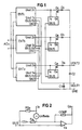
- Figure 1 shows a power supply device, the several same ENTa single power supplies; ENTb; ENTc has.
- the output voltages Uout1a, Uout1b and Uout1c can be, for example, a 5 volt Act voltage, which is regulated via a duty cycle control becomes.
- With the output voltages Uout2a, Uout2b and Uout2c is, for example, a 12 volt voltage.
- the individual power supplies ENTa; ENTb; ENTc are parallel on the input side switched and to an input AC voltage ACin connected. On the output side, the individual power supplies are ENTa, ENTb, ENTc per output voltage also generated in parallel switched. Via a parallel 5-volt bus line IBUS5V the individual power supplies with regard to the 5 volt output voltage parallelized. An even distribution of electricity over the Individual power supplies ENTa, ENTb, ENTc are carried out via an acquisition of the 5 volt output or primary input current, averaging via the 5-volt bus line IBUS5V and readjustment of the primary duty cycle according to the voltage the 5-volt bus line IBUS5V (compare the aforementioned Document DE 3 941 052 C1).
- a decoupling of the individual power supplies regarding the 5 volt output voltage is within the Accept boxes for the individual power supplies. It is for them 5 volt output voltage is not shown separately in FIG. 1.
- the 5-volt output voltage is via an output capacitor C1 to an output voltage UOUT1 of the power supply device smoothed.
- the 12 volt voltages of the individual power supplies ENTa; ENTb; ENTc are in each case before the parallel connection via linear readjustment units, as mentioned, adjusted.
- the linear readjustment units have linearly controllable actuators Qa, Qb, Qc on.
- the actuators Qa, Qb, Qc are in series with decoupling diodes Da, Db, Dc switched.
- the decoupling diodes Da, Db, Dc are polarized in the direction of the output of the power supply device.
- Each readjustment unit has a box in FIG. 1 shown circuit part, the inside of which in the Figure 2 is shown in more detail. Overall, it is the case that circuit part shown as a box to be readjusted Output current is fed through a tap circuit.
- the supply line is via lines Ia, Ib, Ic.
- the tap can be done for example by means of a shunt resistor.
- the actuators Qa, Qb, Qc are connected via lines Ga, Gb, Gc controlled from a respective box.
- a line IBUS connects the individual boxes of the readjustment units.
- FIG. 2 shows an example of the structure of the one with ENTa designated box belonging to the power supply from the figure 1 shown in more detail.
- the display can be analogous to the boxes for those designated in FIG. 1 by ENTb and ENTc Individual power supplies are transferred.
- a comparator Va is shown in the box shown in more detail, the one with a Comp Comp to eliminate the tendency to oscillate is connected.
- Comparator Va can around an operational amplifier with a negative and a act positive input.
- Comp Comp is between the negative input and the output of the comparator Va switched.
- the output of the comparator Va is connected to the line Ga.
- the negative input of comparator Va is over one Resistor Ra switched to a negative voltage potential.
- the negative voltage potential is -12 volts.
- a sink Uoffseta connected at the negative input of comparator Va.
- the connection is made via one of the Connection sides of the sink. With the other connection side is the Uoffseta valley with a connection side of a resistance component RSa and connected to line Ia.
- connection side of the resistance component is RSa with a positive input from the comparator Va and with the IBUS line connected.
- the Uoffseta depression can be caused, for example, by a resistor be formed, together with the resistor Ra a voltage divider forms.
- the Uoffseta valley could, for example also formed by a zener diode and two resistors be.
- the comparator Va carries out a comparison of a target current an actual current through.
- the target current is at the positive input and the actual current is at the negative input of the comparator Va an.
Landscapes
- Engineering & Computer Science (AREA)
- Power Engineering (AREA)
- Physics & Mathematics (AREA)
- Electromagnetism (AREA)
- General Physics & Mathematics (AREA)
- Radar, Positioning & Navigation (AREA)
- Automation & Control Theory (AREA)
- Direct Current Feeding And Distribution (AREA)
- Control Of Voltage And Current In General (AREA)
- Dc-Dc Converters (AREA)
- Control Of Electrical Variables (AREA)
- Fluid-Damping Devices (AREA)
- Apparatus For Radiation Diagnosis (AREA)
- Valve Device For Special Equipments (AREA)
- Supply And Distribution Of Alternating Current (AREA)
- Stand-By Power Supply Arrangements (AREA)
Claims (6)
- Dispositif d'alimentation en courant, formé par des blocs d'alimentation individuels (ENTa; ENTb; ENTc) identiques montés en parallèle de manière découplée les uns par rapport aux autres,a) qui sont pourvus de sorties pour des tensions de sortie couplées (par exemple ENTa: Uout1a, Uout2a) dont une (par exemple Uout1a) est, à chaque fois, réglée par une commande basée sur le taux d'impulsions et dont les autres (par exemple Uout2a) sont ajustées par des unités d'ajustage linéaire comprenant un organe de réglage à commande linéaire (par exemple Qa) et un comparateur (par exemple Va) relié à une entrée de commande de l'organe de réglage (par exemple Qa), lequel comparateur compare une grandeur électrique de consigne à une grandeur électrique effective et commande l'organe de réglage (par exemple Qa) en conséquence, en fonction du résultat de la comparaison,b) auxquels est associé, avant chacun des organes de réglage à commande linéaire (par exemple Qa), un circuit de prélèvement pour le prélèvement, en tant que grandeur électrique effective, d'un courant de sortie (par exemple Uout2a) couplé associé à l'organe de réglage (par exemple Qa), lequel circuit de prélèvement est relié, en même temps, avec les premières bornes d'un composant à résistance (par exemple RSa) et d'un réducteur de courant (par exemple Uoffseta), respectivement, le réducteur de courant (par exemple Uoffseta) étant relié, par une seconde borne, à une entrée pour la grandeur effective du comparateur (par exemple Va) et le composant à résistance (par exemple RSa) étant relié, par une seconde borne, à une entrée pour la grandeur de consigne du comparateur (par exemple Va) et, en même temps, à une ligne collectrice (IBUS) qui est reliée, en même temps, aux secondes bornes respectives des composants à résistance (RSb; RSc) des unités d'ajustage des autres blocs d'alimentation individuels respectifs montés en parallèle (par exemple ENTb; ENTc) et donne ainsi une valeur de consigne du courant qui est obtenue en faisant la moyenne de toutes les valeurs effectives du courant, etc) dont les circuits de prélèvement associés respectifs contiennent des réducteurs de courant dimensionnés de manière à provoquer, à chaque fois, une erreur définie de syntonisation de la comparaison des courants de consigne et effectif.
- Dispositif d'alimentation en courant selon la revendication 1, caractérisé en ce que les organes de réglage (par exemple Qa) sont formés par des transistors MOS dont la diode de drain est située dans le sens contraire à la sortie du dispositif d'alimentation en courant, et en ce que le découplage réciproque des blocs d'alimentation individuels (ENTa; ENTb; ENTc) pour des tensions de sortie (par exemple Uout2a, Uout2b, Uout2c) toutes identiques les unes aux autres est produit par des diodes de découplage (par exemple Da, Db, Dc) qui sont polarisées dans le sens de conduction d'un courant de sortie correspondant respectif et qui sont interconnectées, sur le côté de sortie, pour former une sortie commune pour une tension accumulée de sortie (par exemple UOUT2) résultante.
- Dispositif d'alimentation en courant selon la revendication 1, caractérisé en ce que les organes de réglage (par exemple Qa) sont formés par des transistors MOS dont la diode de drain est située dans le sens de la sortie du dispositif d'alimentation en courant, et en ce que les organes de réglage (par exemple Qa; Qb; Qc) pour les tensions de sortie (par exemple Uout2a, Uout2b, Uout2c) identiques pour chacun des blocs d'alimentation individuels (ENTa; ENTb; ENTc) sont interconnectés, sur le côté de la sortie, de manière à former une sortie commune pour une tension accumulée de sortie (par exemple UOUT2) résultante.
- Alimentation en courant selon l'une des revendications 1 à 3, caractérisée en ce que le réducteur de courant (par exemple Uoffseta) pour une grandeur électrique effective prélevée (par exemple Uout2a) est formé par une résistance.
- Alimentation en courant selon l'une des revendications 1 à 3, caractérisée en ce que le réducteur de courant (par exemple Uoffseta) pour une grandeur électrique effective prélevée (la) est formé par au moins une diode Zener.
- Dispositif d'alimentation en courant selon l'une des revendications précédentes, caractérisé en ce que, pour obtenir une redondance, on prévoit, par rapport au nombre de blocs d'alimentation individuels (par exemple ENTa; ENTb) nécessaires pour une application, un bloc d'alimentation individuel supplémentaire (par exemple ENTc).
Applications Claiming Priority (3)
| Application Number | Priority Date | Filing Date | Title |
|---|---|---|---|
| DE19506405 | 1995-02-23 | ||
| DE19506405A DE19506405C1 (de) | 1995-02-23 | 1995-02-23 | Stromversorgungseinrichtung |
| PCT/DE1996/000178 WO1996026571A1 (fr) | 1995-02-23 | 1996-02-06 | Dispositif d'alimentation en courant |
Publications (2)
| Publication Number | Publication Date |
|---|---|
| EP0811267A1 EP0811267A1 (fr) | 1997-12-10 |
| EP0811267B1 true EP0811267B1 (fr) | 1998-11-11 |
Family
ID=7754890
Family Applications (1)
| Application Number | Title | Priority Date | Filing Date |
|---|---|---|---|
| EP96901237A Expired - Lifetime EP0811267B1 (fr) | 1995-02-23 | 1996-02-06 | Dispositif d'alimentation en courant |
Country Status (8)
| Country | Link |
|---|---|
| US (1) | US5864476A (fr) |
| EP (1) | EP0811267B1 (fr) |
| CN (1) | CN1068146C (fr) |
| AT (1) | ATE173362T1 (fr) |
| DE (2) | DE19506405C1 (fr) |
| ES (1) | ES2125093T3 (fr) |
| TW (1) | TW293104B (fr) |
| WO (1) | WO1996026571A1 (fr) |
Families Citing this family (8)
| Publication number | Priority date | Publication date | Assignee | Title |
|---|---|---|---|---|
| DE19722127C1 (de) * | 1997-05-27 | 1998-07-02 | Siemens Nixdorf Inf Syst | Schaltungsanordnung einer eine gekoppelte, linear nachgeregelte Ausgangsspannung liefernden Stromversorgungseinheit |
| US6191566B1 (en) | 1999-08-26 | 2001-02-20 | Lucent Technologies Inc. | Board mountable power supply module with multi-function control pin |
| JP2002135975A (ja) * | 2000-10-30 | 2002-05-10 | Furukawa Battery Co Ltd:The | 電源システム |
| EP1349254B1 (fr) * | 2002-03-29 | 2012-03-28 | POWER ONE ITALY S.p.A. | Redresseur de puissance avec moyens de coupure de alimentation de puissance |
| JP2006268656A (ja) * | 2005-03-25 | 2006-10-05 | Elpida Memory Inc | 内部電源制御方法、内部電源回路、および半導体装置 |
| US7732941B2 (en) * | 2007-03-29 | 2010-06-08 | Intersil Americas Inc. | Multi-module current sharing scheme |
| CN103997276B (zh) * | 2009-12-18 | 2018-03-27 | 株式会社电装 | 用于电功率转换电路的驱动器件 |
| TW202015305A (zh) * | 2018-10-09 | 2020-04-16 | 和碩聯合科技股份有限公司 | 電子裝置及其電源供應模組 |
Family Cites Families (9)
| Publication number | Priority date | Publication date | Assignee | Title |
|---|---|---|---|---|
| DE278011C (fr) * | ||||
| JPS58215928A (ja) * | 1982-06-10 | 1983-12-15 | 富士電機株式会社 | 安定化電源の並列運転方式 |
| JPS5999930A (ja) * | 1982-11-26 | 1984-06-08 | 三菱電機株式会社 | 電源システム |
| DD278011A1 (de) * | 1988-12-12 | 1990-04-18 | Koepenick Funkwerk Veb | Schaltungsanordnung zur stromausgleichsregelung bei ausgangsseitiger parallelschaltung von stabilisierten leistungsquellen |
| FR2650410B1 (fr) * | 1989-07-28 | 1991-10-11 | Bull Sa | Dispositif convertisseur d'energie a sorties multiples |
| DE3932437C1 (fr) * | 1989-09-28 | 1990-10-04 | Bicc-Vero Elektronics Gmbh, 2800 Bremen, De | |
| DE3941052C1 (fr) * | 1989-12-12 | 1991-05-29 | Siemens Ag, 1000 Berlin Und 8000 Muenchen, De | |
| DE4025718A1 (de) * | 1990-08-14 | 1992-02-27 | Kloeckner Moeller Gmbh | Verfahren zur symmetrischen lastverteilung bei ausgangsseitig parallelgeschalteten stromversorgungsgeraeten |
| US5319536A (en) * | 1991-12-17 | 1994-06-07 | International Business Machines Corporation | Power system for parallel operation of AC/DC convertrs |
-
1995
- 1995-02-23 DE DE19506405A patent/DE19506405C1/de not_active Expired - Fee Related
-
1996
- 1996-02-02 TW TW085101306A patent/TW293104B/zh not_active IP Right Cessation
- 1996-02-06 EP EP96901237A patent/EP0811267B1/fr not_active Expired - Lifetime
- 1996-02-06 DE DE59600809T patent/DE59600809D1/de not_active Expired - Lifetime
- 1996-02-06 US US08/894,537 patent/US5864476A/en not_active Expired - Lifetime
- 1996-02-06 WO PCT/DE1996/000178 patent/WO1996026571A1/fr not_active Ceased
- 1996-02-06 ES ES96901237T patent/ES2125093T3/es not_active Expired - Lifetime
- 1996-02-06 CN CN96192073A patent/CN1068146C/zh not_active Expired - Fee Related
- 1996-02-06 AT AT96901237T patent/ATE173362T1/de not_active IP Right Cessation
Also Published As
| Publication number | Publication date |
|---|---|
| EP0811267A1 (fr) | 1997-12-10 |
| CN1068146C (zh) | 2001-07-04 |
| ATE173362T1 (de) | 1998-11-15 |
| DE59600809D1 (de) | 1998-12-17 |
| WO1996026571A1 (fr) | 1996-08-29 |
| CN1176025A (zh) | 1998-03-11 |
| ES2125093T3 (es) | 1999-02-16 |
| TW293104B (fr) | 1996-12-11 |
| DE19506405C1 (de) | 1996-03-07 |
| US5864476A (en) | 1999-01-26 |
Similar Documents
| Publication | Publication Date | Title |
|---|---|---|
| DE69226340T2 (de) | Leistungssystem zum Parallelbetrieb von Wechselstrom-Gleichstrom-Umwandlern | |
| DE10214190B4 (de) | Stromversorgung mit mehreren parallel geschalteten Schaltnetzteilen | |
| DE3015610A1 (de) | Schaltung zur regelung eines gleichstroms | |
| DE3613895C2 (fr) | ||
| EP0143955A1 (fr) | Dispositif d'alimentation | |
| DE3320885A1 (de) | Parallelbetriebssysteme fuer stabilisierte leistungsquellen | |
| DE19506405C1 (de) | Stromversorgungseinrichtung | |
| DE69824751T2 (de) | Regler | |
| EP0708998B1 (fr) | Systeme d'alimentation en tension continue fonctionnant en tampon | |
| DE2543537C3 (de) | Anordnung zur Spannungsregelung eines Solargenerators | |
| EP1327290B1 (fr) | Ensemble circuit pour surveiller et/ou regler des tensions d'alimentation | |
| EP0881735B1 (fr) | Disposition de circuit pour une unité d'alimentation de puissance | |
| DE3941052C1 (fr) | ||
| DE2239796A1 (de) | Auf einen ueberspannungszustand ansprechende anordnung zur erzeugung eines frequenzerhoehungs-steuersignales | |
| DE4037722C1 (en) | Current supply circuitry with no mains transformer - has controlled transistor acting as limiting stage across output of rectifier stage | |
| EP0985260B1 (fr) | Circuit de commutation pour unite d'alimentation en courant fournissant des tensions de sortie couplees et rajustees de maniere lineaire | |
| DE3891380C2 (de) | Verstärker mit vier Transistoren, die in einer Brückenschaltung miteinander verbunden sind | |
| EP0881736A2 (fr) | Disposition de circuit pour une unité d'alimentation de puissance | |
| EP3830944B1 (fr) | Source de tension longitudinale commutable, système de transmission de courant continu pourvu de la source de tension longitudinale et procédé pour faire fonctionner une source de tension longitudinale | |
| DE19710484C2 (de) | Kontaktloses Relais | |
| DE4009077C2 (fr) | ||
| EP0589228A1 (fr) | Amplificateur de puissance HF | |
| AT412684B (de) | Vorrichtung zur verlustarmen symmetrierung der kondensatorspannungen bei leistungselektronischen konvertern mit spannungszwischenkreis | |
| DE102011122076B4 (de) | Schaltung zur Kompensation von Spannungsänderungen an geschalteten stromübernehmenden Baugruppen zur Anwendung in Bussystemen | |
| EP0572452B1 (fr) | Bloc d'alimentation secteur a alimentation polyphasee |
Legal Events
| Date | Code | Title | Description |
|---|---|---|---|
| PUAI | Public reference made under article 153(3) epc to a published international application that has entered the european phase |
Free format text: ORIGINAL CODE: 0009012 |
|
| 17P | Request for examination filed |
Effective date: 19970806 |
|
| AK | Designated contracting states |
Kind code of ref document: A1 Designated state(s): AT BE CH DE ES FR GB IT LI NL SE |
|
| GRAG | Despatch of communication of intention to grant |
Free format text: ORIGINAL CODE: EPIDOS AGRA |
|
| 17Q | First examination report despatched |
Effective date: 19980220 |
|
| GRAG | Despatch of communication of intention to grant |
Free format text: ORIGINAL CODE: EPIDOS AGRA |
|
| GRAH | Despatch of communication of intention to grant a patent |
Free format text: ORIGINAL CODE: EPIDOS IGRA |
|
| GRAH | Despatch of communication of intention to grant a patent |
Free format text: ORIGINAL CODE: EPIDOS IGRA |
|
| GRAA | (expected) grant |
Free format text: ORIGINAL CODE: 0009210 |
|
| AK | Designated contracting states |
Kind code of ref document: B1 Designated state(s): AT BE CH DE ES FR GB IT LI NL SE |
|
| REF | Corresponds to: |
Ref document number: 173362 Country of ref document: AT Date of ref document: 19981115 Kind code of ref document: T |
|
| REG | Reference to a national code |
Ref country code: CH Ref legal event code: NV Representative=s name: SIEMENS SCHWEIZ AG Ref country code: CH Ref legal event code: EP |
|
| REF | Corresponds to: |
Ref document number: 59600809 Country of ref document: DE Date of ref document: 19981217 |
|
| ITF | It: translation for a ep patent filed | ||
| GBT | Gb: translation of ep patent filed (gb section 77(6)(a)/1977) |
Effective date: 19990119 |
|
| ET | Fr: translation filed | ||
| REG | Reference to a national code |
Ref country code: ES Ref legal event code: FG2A Ref document number: 2125093 Country of ref document: ES Kind code of ref document: T3 |
|
| PLBE | No opposition filed within time limit |
Free format text: ORIGINAL CODE: 0009261 |
|
| STAA | Information on the status of an ep patent application or granted ep patent |
Free format text: STATUS: NO OPPOSITION FILED WITHIN TIME LIMIT |
|
| 26N | No opposition filed | ||
| REG | Reference to a national code |
Ref country code: CH Ref legal event code: PUE Owner name: SIEMENS NIXDORF INFORMATIONSSYSTEME AG TRANSFER- F |
|
| REG | Reference to a national code |
Ref country code: CH Ref legal event code: NV Representative=s name: E. BLUM & CO. PATENTANWAELTE |
|
| REG | Reference to a national code |
Ref country code: FR Ref legal event code: TP |
|
| REG | Reference to a national code |
Ref country code: GB Ref legal event code: 732E |
|
| REG | Reference to a national code |
Ref country code: GB Ref legal event code: IF02 |
|
| REG | Reference to a national code |
Ref country code: CH Ref legal event code: PFA Owner name: FUJITSU SIEMENS COMPUTERS GMBH Free format text: FUJITSU SIEMENS COMPUTERS GMBH#OTTO-HAHN-RING 6#81739 MUENCHEN (DE) -TRANSFER TO- FUJITSU SIEMENS COMPUTERS GMBH#OTTO-HAHN-RING 6#81739 MUENCHEN (DE) |
|
| PGFP | Annual fee paid to national office [announced via postgrant information from national office to epo] |
Ref country code: ES Payment date: 20100225 Year of fee payment: 15 Ref country code: CH Payment date: 20100224 Year of fee payment: 15 |
|
| PGFP | Annual fee paid to national office [announced via postgrant information from national office to epo] |
Ref country code: IT Payment date: 20100225 Year of fee payment: 15 |
|
| PGFP | Annual fee paid to national office [announced via postgrant information from national office to epo] |
Ref country code: BE Payment date: 20100223 Year of fee payment: 15 Ref country code: AT Payment date: 20100120 Year of fee payment: 15 |
|
| PGFP | Annual fee paid to national office [announced via postgrant information from national office to epo] |
Ref country code: NL Payment date: 20100223 Year of fee payment: 15 |
|
| PGFP | Annual fee paid to national office [announced via postgrant information from national office to epo] |
Ref country code: SE Payment date: 20100226 Year of fee payment: 15 |
|
| REG | Reference to a national code |
Ref country code: GB Ref legal event code: 746 Effective date: 20110527 |
|
| BERE | Be: lapsed |
Owner name: *FUJITSU SIEMENS COMPUTERS G.M.B.H. Effective date: 20110228 |
|
| REG | Reference to a national code |
Ref country code: NL Ref legal event code: V1 Effective date: 20110901 |
|
| REG | Reference to a national code |
Ref country code: CH Ref legal event code: PL |
|
| REG | Reference to a national code |
Ref country code: SE Ref legal event code: EUG |
|
| PG25 | Lapsed in a contracting state [announced via postgrant information from national office to epo] |
Ref country code: CH Free format text: LAPSE BECAUSE OF NON-PAYMENT OF DUE FEES Effective date: 20110228 Ref country code: LI Free format text: LAPSE BECAUSE OF NON-PAYMENT OF DUE FEES Effective date: 20110228 |
|
| PG25 | Lapsed in a contracting state [announced via postgrant information from national office to epo] |
Ref country code: AT Free format text: LAPSE BECAUSE OF NON-PAYMENT OF DUE FEES Effective date: 20110206 Ref country code: BE Free format text: LAPSE BECAUSE OF NON-PAYMENT OF DUE FEES Effective date: 20110228 |
|
| PG25 | Lapsed in a contracting state [announced via postgrant information from national office to epo] |
Ref country code: IT Free format text: LAPSE BECAUSE OF NON-PAYMENT OF DUE FEES Effective date: 20110206 Ref country code: NL Free format text: LAPSE BECAUSE OF NON-PAYMENT OF DUE FEES Effective date: 20110901 |
|
| REG | Reference to a national code |
Ref country code: DE Ref legal event code: R082 Ref document number: 59600809 Country of ref document: DE Representative=s name: EPPING HERMANN FISCHER, PATENTANWALTSGESELLSCH, DE Effective date: 20111229 Ref country code: DE Ref legal event code: R081 Ref document number: 59600809 Country of ref document: DE Owner name: FUJITSU TECHNOLOGY SOLUTIONS INTELLECTUAL PROP, DE Free format text: FORMER OWNER: FUJITSU SIEMENS COMPUTERS GMBH, 80807 MUENCHEN, DE Effective date: 20111229 |
|
| REG | Reference to a national code |
Ref country code: ES Ref legal event code: FD2A Effective date: 20120411 |
|
| PG25 | Lapsed in a contracting state [announced via postgrant information from national office to epo] |
Ref country code: ES Free format text: LAPSE BECAUSE OF NON-PAYMENT OF DUE FEES Effective date: 20110207 |
|
| PGFP | Annual fee paid to national office [announced via postgrant information from national office to epo] |
Ref country code: FR Payment date: 20120306 Year of fee payment: 17 |
|
| PGFP | Annual fee paid to national office [announced via postgrant information from national office to epo] |
Ref country code: DE Payment date: 20120221 Year of fee payment: 17 |
|
| PGFP | Annual fee paid to national office [announced via postgrant information from national office to epo] |
Ref country code: GB Payment date: 20120224 Year of fee payment: 17 |
|
| PG25 | Lapsed in a contracting state [announced via postgrant information from national office to epo] |
Ref country code: SE Free format text: LAPSE BECAUSE OF NON-PAYMENT OF DUE FEES Effective date: 20110207 |
|
| GBPC | Gb: european patent ceased through non-payment of renewal fee |
Effective date: 20130206 |
|
| REG | Reference to a national code |
Ref country code: FR Ref legal event code: ST Effective date: 20131031 |
|
| REG | Reference to a national code |
Ref country code: DE Ref legal event code: R119 Ref document number: 59600809 Country of ref document: DE Effective date: 20130903 |
|
| PG25 | Lapsed in a contracting state [announced via postgrant information from national office to epo] |
Ref country code: FR Free format text: LAPSE BECAUSE OF NON-PAYMENT OF DUE FEES Effective date: 20130228 Ref country code: GB Free format text: LAPSE BECAUSE OF NON-PAYMENT OF DUE FEES Effective date: 20130206 Ref country code: DE Free format text: LAPSE BECAUSE OF NON-PAYMENT OF DUE FEES Effective date: 20130903 |