EP0815577B1 - Schmelzbarer widerstand für fehlerstrom und verfahren dafür - Google Patents
Schmelzbarer widerstand für fehlerstrom und verfahren dafür Download PDFInfo
- Publication number
- EP0815577B1 EP0815577B1 EP96906648A EP96906648A EP0815577B1 EP 0815577 B1 EP0815577 B1 EP 0815577B1 EP 96906648 A EP96906648 A EP 96906648A EP 96906648 A EP96906648 A EP 96906648A EP 0815577 B1 EP0815577 B1 EP 0815577B1
- Authority
- EP
- European Patent Office
- Prior art keywords
- film
- line
- fault
- fuse
- inch
- Prior art date
- Legal status (The legal status is an assumption and is not a legal conclusion. Google has not performed a legal analysis and makes no representation as to the accuracy of the status listed.)
- Expired - Lifetime
Links
Images

Classifications
-
- H—ELECTRICITY
- H01—ELECTRIC ELEMENTS
- H01H—ELECTRIC SWITCHES; RELAYS; SELECTORS; EMERGENCY PROTECTIVE DEVICES
- H01H85/00—Protective devices in which the current flows through a part of fusible material and this current is interrupted by displacement of the fusible material when this current becomes excessive
- H01H85/02—Details
- H01H85/04—Fuses, i.e. expendable parts of the protective device, e.g. cartridges
-
- H—ELECTRICITY
- H01—ELECTRIC ELEMENTS
- H01H—ELECTRIC SWITCHES; RELAYS; SELECTORS; EMERGENCY PROTECTIVE DEVICES
- H01H85/00—Protective devices in which the current flows through a part of fusible material and this current is interrupted by displacement of the fusible material when this current becomes excessive
- H01H85/02—Details
- H01H85/04—Fuses, i.e. expendable parts of the protective device, e.g. cartridges
- H01H85/041—Fuses, i.e. expendable parts of the protective device, e.g. cartridges characterised by the type
- H01H85/048—Fuse resistors
-
- H—ELECTRICITY
- H01—ELECTRIC ELEMENTS
- H01H—ELECTRIC SWITCHES; RELAYS; SELECTORS; EMERGENCY PROTECTIVE DEVICES
- H01H85/00—Protective devices in which the current flows through a part of fusible material and this current is interrupted by displacement of the fusible material when this current becomes excessive
- H01H85/02—Details
- H01H85/04—Fuses, i.e. expendable parts of the protective device, e.g. cartridges
- H01H85/041—Fuses, i.e. expendable parts of the protective device, e.g. cartridges characterised by the type
- H01H85/046—Fuses formed as printed circuits
-
- H—ELECTRICITY
- H01—ELECTRIC ELEMENTS
- H01H—ELECTRIC SWITCHES; RELAYS; SELECTORS; EMERGENCY PROTECTIVE DEVICES
- H01H85/00—Protective devices in which the current flows through a part of fusible material and this current is interrupted by displacement of the fusible material when this current becomes excessive
- H01H85/02—Details
- H01H85/38—Means for extinguishing or suppressing arc
-
- Y—GENERAL TAGGING OF NEW TECHNOLOGICAL DEVELOPMENTS; GENERAL TAGGING OF CROSS-SECTIONAL TECHNOLOGIES SPANNING OVER SEVERAL SECTIONS OF THE IPC; TECHNICAL SUBJECTS COVERED BY FORMER USPC CROSS-REFERENCE ART COLLECTIONS [XRACs] AND DIGESTS
- Y10—TECHNICAL SUBJECTS COVERED BY FORMER USPC
- Y10T—TECHNICAL SUBJECTS COVERED BY FORMER US CLASSIFICATION
- Y10T29/00—Metal working
- Y10T29/49—Method of mechanical manufacture
- Y10T29/49002—Electrical device making
- Y10T29/49082—Resistor making
Definitions
- power-semiconductors transistors, thyristors, SCRs etc.
- An illustration is the power drivers for motors such as are used on electric trains.
- the power-semiconductors associated with the control circuits or drive circuits occasionally short internally, which can cause the portion of the circuit that is in the short circuit path caused by the shorted power-semiconductor to be exposed suddenly to a very high fault current and fault voltage.
- fault current fusing devices which operate at relatively high currents and that can interrupt relatively high voltages are quite large, and/or expensive, and/or slow-acting, and/or have other disadvantages.
- Simple fuses are shown in GB-A-1184056, US-A-3401452 and EP-A-0270954.
- the fuse element is formed as an electrically conducting layer of silver in particular a flake form mixed with glass particles sandwiched between two insulating layers.
- the fuse is formed by a metal layer, typically gold, deposited on a substrate and covered with a layer of glass.
- the fuse is formed by a conductive track deposited on a ceramic substrate and covered with a silicone resin film.
- a fault current fusing resistor operates very quickly when exposed to the described (and other) relatively high fault currents and relatively high fault AC/DC voltages.
- the device opens (clears) in a way that is controlled, contained, and nonexplosive, thus substantially safe, and that does not generate debris. There is substantially no uncontained arcing, or no arcing at all.
- the device When the device is placed in a power-semiconductor circuit, or the like, it operates for great periods of time with only the normal low current passing through it. However, upon sudden occurrence of a fault current, the step change in current flow results in the stated very fast cessation of flow of the fault current.
- a fuse comprises
- a method of protecting a circuit portion from short circuits and other electrical faults comprises connecting in circuit with said circuit portion a fault current fusing resistor having an elongate line of resistive film having a substantially uniform width on a substrate with a confining and sealing means closely confining and sealing said film to prevent escape of vapours of said film by remaining intact, unbroken and unruptured when a fault occurs in said circuit portion, and so selecting said film that upon occurrence of said fault there are formed many breaks in said line, said breaks extending transversely of said line and being spaced from each other longitudinally of said line.
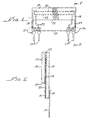
- an elongate resistive element 10 is extended between terminal means 11, 11a (FIG. 1).
- the element 10 is contained and sealed-in by containing and sealing means 12 (FIG. 2) that are sufficiently strong to withstand the forces related to the heating and opening of the resistive element caused by fault current.
- Resistive element 10 is preferably a screen-printed resistive thick-film composition on a base or substrate 13, the latter also forming part of the containing and sealing means described below.
- the resistive element 10 may be formed by vacuum deposition, sputtered deposition, "inkjet", or other similar means.
- the thick-film screen-printed element 10 is a palladium-silver composition.
- the element 10 is screen-printed thin, using a 325 or 400 mesh screen.
- An example of the palladium-silver compositions that may be employed is "Ferro 850" series, sold by Ferro Corporation, Electronic Materials Division, Santa Barbara, California.
- the composition and shape of the resistive element 10 are such that it has a relatively low resistance of usually under 30 ohms, preferably 10 ohms down to 1.0 or 0.5 ohm (or even sonewhat lower).
- the resistance of resistive element 10 is not down to a small fraction of an ohm, for example, a few milliohms.
- the resistivity of the material forming the resistive element 10 is typically in the fractional ohms per square.
- this is made sufficiently long to withstand the applied voltage after the fault current has ceased, but sufficiently short to prevent the resistance from being excessively high and sufficiently short for proper operation.
- a line length of less than 1 inch is preferred. The lower the voltage rating of the device, the shorter the line length necessary for proper operation.
- the narrower lines are preferred insofar as operation during a fault is concerned.
- a 0.01 inch line width is preferred over the 0.03 inch line width.
- the wider (e.g. 0.03 inch) line spreads the power over a greater surface area and aids in heat dissipation.
- a narrower line such as the 0.01 inch wide line is preferred.
- a wider line such as the 0.03 inch wide line is preferred.
- Higher resistance values (such as 10 ohms) in the range specified in the preceding paragraph limit the magnitude of the fault current during the moment just before the FCFR opens.
- Configurations that may be employed include arcuate and meandering, provided there is a shallow angle that avoids a small dimension between adjacent lines in the meandering pattern so that there will not be arcing between loops.
- a straight line is preferred.
- the line may also be arcuate (as stated) or a wide angle that is preferably obtuse.
- the line (forming element 10) should progress forwardly (toward the opposite terminal) instead of doubling back. In any event, there may be no doubling back where different parts of the adjacent lines are so close together as to cause arcing.
- the size of the actual resistive element 10, in a specific example given for purposes of illustration, not limitation, is about 0.680 inch long, having a width of 0.030 inch.
- the resistance of this specific example element is 10 ohms.
- the size of substrate 13 is 0.80 inch long by 0.50 inch high.
- the line of resistive film in the present example, is 0.0004 inch to 0.001 inch thick (fired thickness).
- terminal means 11 may be a wide variety of terminals including (for example) terminals generally in line with the resistive element 10. It is not necessary that the terminals connect to the substrate 13 mechanically, but this is preferred for the present embodiment, which has solder attachment of the terminals.
- the illustrated screen-printed traces 14 and pads 16 form part of the terminal means 11 (FIG. 1), being located adjacent the ends of substrate 13 with the traces generally parallel to the ends of the substrate.
- Traces 14 and pads 16 are simultaneously screen-printed of a low resistivity material, preferably having a resistivity less than 5 milliohms per square.
- An example of this is DuPont 9770.
- DuPont 9770 is a platinum-silver composition.
- the terminal means in the illustrated example include jaw-type terminal pins 17 that clamp on pads 16, 18 and are soldered thereon.
- the pins 17 are prevented from heating excessively, not only by the high conductivity of the traces 14 and pads 16, but also because the resistive element 10 is spaced away from the lower edge of the substrate 13, being relatively near the upper edge thereof.
- the resistive element 10 is spaced away from the lower edge of the substrate 13, being relatively near the upper edge thereof.
- the thermal gradient is increased by thinness of the substrate.
- the illustrated preferred such means comprises the substrate 13 which therefore (in the preferred form) serves not only for application of the films but as part of the containing and sealing means. It further comprises a lid 19 (FIGS. 1 and 2) that is preferably positioned with its top and side margins registered with the upper and vertical margins of substrate 13 and with its lower edge 21 spaced from resistive element 10.
- An exemplary material forming the substrate 13 and lid 19 is aluminum oxide.
- Elements 13, 19 may each have a thickness of 0.030 inch. When the pressures are higher, each is made 0.040 inch thick. Even these relatively thin layers, formed of brittle aluminum oxide (for example), will contain the pressures resulting from large current flows through resistive element 10.
- the containing and sealing means 12 further comprises sealing and connecting material 22 (FIG. 2) that fills the entire space between the facing surfaces of elements 13, 19.
- the preferred such material is epoxy adhesive. Because it fills the entire space, except that space occupied by the films, there is substantially no air between the elements 13, 19 (there may be very small air bubbles in the epoxy).
- the resistive element 10 is covered with an overglaze (glass layer) 23.
- This glass layer is preferably screen-printed and is then fired.
- An exemplary material is DuPont 9137. There are preferably two passes during screen-printing, using a 200 mesh screen, fired after each pass at 550°C to a highly glassy finish.
- glass layer 23 is substantially larger than resistive element 10 so that is extends substantially beyond the sides and ends of the resistive element.
- the resistive element 10 increases in width by typically less than 10% along each side. There may be no increase in width.
- the ceramic substrate and lid, the epoxy, and (preferably) the glass layer cooperate to form an effective containing and sealing means 12 that (as above stated) prevent explosion of the FCFR and prevent blowouts. There is no debris after the fuse opens, and the product is characterized by a high degree of safety.
- the lower edge 21 of lid 19 is much lower than that illustrated in FIGS. 1 and 2, being adjacent the upper portions of the jaws of pins 17.
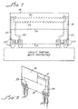
- the present article or device (preferably the preferred form shown in the drawings and described in detail above) is mounted on a circuit board or otherwise connected in series relationship with the components or circuit board traces to be protected against short circuit current.
- Fig. 7. In the exemplary situation described at the beginning of this specification, this is a circuit for a power-semiconductor.
- the present FCFR is connected in series with the potential short circuit current path of the power-semiconductor circuit.
- the present invention includes (in one of its aspects) the combination of a power-semiconductor (and the control circuit associated therewith) with the present FCFR.
- the FCFR in the combination stated in the preceding sentence safely opens at voltages in the range of 150 volts to 1,000 volts AC/DC.
- the present device should not have any portion of the resistive element that is not contained. Thus, for example, there should be no unlidded resistive element portion exposed on the backside (exposed side) of the base or substrate and which is in circuit with the lidded resistive element on the frontside.
- the present FCFR method and article are characterized by results that far exceed any of which applicant has ever heard.
- a practical size of the present FCFR can operate at 2000 volts DC during a fault condition, and clear within 50 micro seconds. This occurs safely, with no breakage or other undesired consequence. It is only a flash of light that is an exteriorly visible consequence of the fault.
- the above-recited palladium-silver Ferro 850 contains palladium and silver and glass. These are present in powder (particle) form, in a suitable vehicle that is present during application to the substrate (as by screen printing) but is driven off by the firing.
- the palladium-silver Ferro 850 is an example of the distinctly preferred form of the present invention, namely certain metal and glass particles (powder) mixed with each other. After firing, the particles of metal are combined with glass in a conductive film. The majority of said film, by weight, is metal particles.
- the second element indicated in the paragraph before last is close containment or encapsulation of the resistive element (such as 10).
- the substrate 13, the lid 19, the sealing and connecting material 22 and (in one form) overglaze 23 accomplish containment in a practical and economical manner.
- effective close containment involves exclusion of substantial air and elimination of substantial voids; air is not desired at or near the resistive element (such as 10) because electric arcing is to be prevented to the maximum extent reasonable.
- the resistive line (such as 10) be quite thin.
- a 325 or 400 mesh screen is used in the screen-printing operation.
- the film after firing is then about 0.0005 inch thick.
- a 200 mesh screen is used the results are less satisfactory.
- the particles of metal in the resistive film 10 are small. Exemplary such particles are about 1 micrometer in size.
- the resistive film (such as 10) after the fault this is determined by first removing the lid 19, epoxy 22 and overglaze 23. Examination by microscope of the resistive film (line) 10 thus exposed reveals the presence of many interruptions, breaks, or discontinuities in the resistive film (line) 10 and extending generally perpendicular to the longitudinal axis of the film (line). The number of such breaks is, applicant believes, related to the magnitude of the voltage present across the FCFR during continuance of the fault. The breaks are spaced from each other longitudinally of the film (line).
- each such break is about 0.0005 inch to 0.003 inch wide.
- These breaks are usually not empty; they contain some residue and also some metal balls or spheres. They also contain some glass, which may be dissolved out by acid in order that the metal may be better seen.
- the breaks may present the appearance of aerial photos of large rivers, in which there are islands and channels--the "river” edges (banks) being not straight but irregular.
- the "rivers” extend substantially the entire distance (0.030 inch in the above-stated example) across the resistive element (such as resistive line 10).
- the metal balls give the appearance, from above, of very large balloons that are hovering over the "rivers"--typically at their "banks".
- the balls have a variety of sizes.
- the breaks (or series thereof) give the appearance of having been produced by pulling the resistive film or line apart, by tensile forces that are longitudinal to the line.
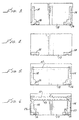
- Fig. 8 is identical to that described above and exemplified below in the specific examples.
- the resistive line (film) 10 is usually not covered by the overglaze 23, although it may be so covered.
- the lid 19 is not present, nor is the sealing and connecting material (epoxy) 22 present.
- a chemically-bonded ceramic substance 26 having sufficient thickness that it will not blow out during a fault condition but will instead contain the pressure resulting from the heating and fusing caused by the high current.
- the preferred form of the substance 26 may be about 0.03 inch thick. However, with some resistive line compositions the thickness is made 0.040 inch-0.060 inch, to prevent blowout.
- Substance 26 is applied in paste form by a syringe and then allowed to air dry. It is then baked and cured. For example, it may (after air drying) be baked at 200°F for 3 hours, then cured at 300°F for one hour. It adheres very tightly to the substrate.
- a preferred such ceramic substance 26 is "Cerama-Dip 538", which is a dielectric coating used for embedding high-temperature resistance wires, etc. Its major constituent is alumina. It is sold by Aremco Products, Inc., of ossining New York.
- FCFR may be packaged in ways desired by the electronics industry.
- it may be packaged as a heatsink-mount device, or a radial lead device, or an axial lead device, or a surface mount device. These devices may have standard physical sizes and footprints.
- the substrate 13a corresponds to substrate 13 except that it is vertically somewhat elongate.
- Low resistivity traces 14a and pads 16a are screen-printed thereon and then fired.
- resistive film (line) 10a is screen-printed thereon and fired.
- Overglaze 23a is screen-printed there over and fired.
- leads or pins 28 are soldered to the pads 16a, and extend parallel to each other outwardly from the substrate 13a.
- Lid 19a (Fig. 13) is then applied by the containing and sealing material (epoxy). Or, ceramic (such as 26) is used.
- a molded package or body 29 (Fig. 14) of synthetic resin is then formed around the assembly shown in Fig. 13, by transfer molding or injection molding.
- the illustrated package 29 has a bolt hole 30 therethrough, so that the device is used as a heatsink-mount device.
- the resistive film (line) 10b corresponds to lines 10 and 10a in composition, etc., but is different in major ways. It is not continuous but segmented. The segments are connected together by low-resistivity pads corresponding in composition to pads (and traces) 14-16 and 14a-16a.
- pads 32, 33, 34 and 35 at the corner portion of substrate 13a (which is the same as the substrate in the previous embodiment).
- Sections 36, 37 and 38 of the resistive film connect respectively between pads 32-33, 33-34, and 34-35. Except for length and orientation, sections 36, 37 and 38 are each identical to resistive film 10.
- the illustrated sections 36, 37 and 38 are at right angles to each other. Their combined lengths are much longer than (for example) the length of line 10a in Fig. 10. Accordingly, the embodiment of Figs. 15-16 can withstand a higher voltage; after the fault condition ends, than can the embodiment of Figs. 9-14.
- the fault voltage drop is distributed along the film line--more specifically along the breaks in such line--so that the longer line provides better isolation of higher fault voltages.
- the low-resistivity corner pads 33,34 reduce the chances that there will be arcing at the corners, or that there will be undesirably large breaks at the corners. No large break is desired; what are wanted are a multiplicity of small breaks such as were described relative to the first embodiment.
- Figs. 15-16 The device of Figs. 15-16 is completed by following the steps shown and described relative to Figs. 11, 12, 13 and 14.
- the result is a high-voltage FCFR, that is small and shaped and packaged as desired, at that clears high currents with amazing speed.
- glass as used in the appended claims includes not only the conventional meaning of that word, but also any ceramic substances having a capability of forming during firing a glass-like matrix in the conductive film, which glass-like matrix functions equivalently to glass so as to achieve the multiple breaks described in detail above. It is also to be understood that under some conditions glass may be "made” during firing from glass-forming ingredients in the deposited material. The glass material may contain reinforcing fillers.
- metal as used in the appended claims, may include also some conductive metal oxides employed together with the metallic metal.
- Construction is as shown in Fig 3 through Fig 6 with ceramic coat encapsulation except substrate is larger and element is slightly longer.
- Construction is as shown in Fig 3, Fig. 4, and Fig. 5. Except larger substrate and slightly larger element. There is no overglaze. This group has a ceramic coating as the encapsulation.
- Construction is as shown in Fig 3 through Fig 6 except 0.015 inch wide (vertical dimension) element with lid. And substrate size is larger and element is slightly larger.
- Construction is as shown in Fig 3 through Fig 6 except 0.015 inch wide (vertical dimension) element overglaze with ceramic coat encapsulation. And substrate size is larger and element is slightly larger.
- Construction is as shown in Fig 3 through Fig 6 except 0.015 inch wide (vertical dimension) element, overglaze and ceramic coat encapsulation. And substrate size is larger and element is slightly larger.
Landscapes
- Emergency Protection Circuit Devices (AREA)
- Apparatuses And Processes For Manufacturing Resistors (AREA)
- Fuses (AREA)
- Thermistors And Varistors (AREA)
- Control Of Electrical Variables (AREA)
- Non-Adjustable Resistors (AREA)
- Details Of Resistors (AREA)
- Crystals, And After-Treatments Of Crystals (AREA)
- Glass Compositions (AREA)
Claims (27)
- Sicherung mit:wobei die streifenförmige Schicht (10) und die Aufnahme- und Dichtungseinrichtung (19, 26) derart ausgewählt sind, daß beim Auftreten einer elektrischen Störung mit einer ausreichenden Größe, durch die veranlaßt wird, daß die streifenförmige Schicht (10) schmilzt, die Aufnahme- und Dichtungseinrichtung (19, 26) eine ausreichende Festigkeit besitzt, so daß sie während des Auftretens und nach dem Auftreten einer elektrischen Störung intakt bleibt, nicht bricht und nicht unterbrochen wird, und, wenn eine elektrische Störung mit einer ausreichenden Größe auftritt, so daß die streifenförmige Schicht (10) schmilzt, viele Unterbrechungen oder Brüche in der streifenförmigen Schicht (10) erzeugt werden, die sich in Querrichtung der streifenförmigen Schicht erstrecken und in ihrer Längsrichtung beabstandet sind.(a) einer länglichen, streifenförmigen elektrischen Widerstandsschicht (10) auf einem Substrat (13), wobei die Schicht Metallpartikel und Glas aufweist;(b) einer Anschlußeinrichtung (14, 17), die mit der längliche, streifenförmigen Schicht (10) an entgegengesetzten Endabschnitten davon verbunden ist; und(c) einer um die streifenförmige Schicht (10) herum angeordneten Aufnahme- und Dichtungseinrichtung (19, 26) zum engen Einschließen und Abdichten der gesamten streifenförmigen Schicht (10), wobei die Aufnahme- und Dichtungseinrichtung (19, 26) eine Dichtstruktur aufweist, die mehrfach dicker ist als die elektrische Widerstandsschicht (10);
- Sicherung nach Anspruch 1, wobei die Metallpartikel ein Metallpulver aufweisen, und wobei die Schicht (10) das Metallpulver und das Glas aufweist.
- Sicherung nach Anspruch 2, wobei das Metallpulver in der Schicht (10) Palladium, Palladium und Silber, Gold und Platin oder Silber und Platin ist, oder das Metallpulver Gold und Platin oder Silber und Platin aufweist.
- Sicherung nach einem der vorangehenden Ansprüche, wobei die Aufnahme- und Dichtungseinrichtung eine Überglasur (23) und eine Einrichtung (19, 26) zum Verstärken der Überglasur (23) aufweist, die verhindert, daß die Überglasur während eines elektrischen Störungszustands platzt.
- Sicherung nach Anspruch 4, wobei die Überglasur (23) eine Glasschicht ist, und wobei die Dichtungseinrichtung (19, 26) wesentlich stabiler ist als die Glasschicht.
- Sicherung nach einem der vorangehenden Ansprüche, wobei die Aufnahme- und Dichtungseinrichtung oder die Einrichtung zum Verstärken der Überglasur (23) ein Keramikmaterial (26) ist, das in Pastenform auf der Schicht (10) aufgebracht wird und am Substrat (13) anhaftet und eine ausreichende Dicke hat, so daß es den Druck aushält und bei einem elektrischen Störungszustand nicht platzt.
- Sicherung nach Anspruch 4 oder 5, wobei die Einrichtung zum Verstärken der Überglasur (23) eine Keramikabdeckung (19) und ein Klebemittel zum Befestigen der Abdeckung (19) über der Überglasur am Substrat (13) ist.
- Sicherung nach einem der vorangehenden Ansprüche, wobei die streifenförmige Schicht (10) eine Dicke von etwa 0,01 mm bis 0,025 mm (0,0004 Zoll bis 0,001 Zoll) hat.
- Sicherung nach einem der vorangehenden Ansprüche, wobei die streifenförmige Schicht (10) eine Breite von etwa 0,25 mm bis 0,75 mm (0,01 Zoll bis 0,03 Zoll) hat.
- Sicherung nach einem der vorangehenden Ansprüche, wobei die streifenförmige Schicht (10) eine Länge von weniger als etwa 25,4 mm (1 Zoll) hat.
- Sicherung nach einem der vorangehenden Ansprüche, wobei die streifenförmige Schicht (10) einen Widerstand im Bereich von 0,5 bis 30 Ohm aufweist.
- Sicherung nach einem der vorangehenden Ansprüche, wobei die streifenförmige Schicht (10) eine längliche, streifenförmige Schicht ist, und wobei die streifenförmige Schicht in Abschnitte geteilt ist, die Abschnitte durch eine Schicht mit niedrigem Widerstand elektrisch voneinander getrennt sind, und wobei die Schicht mit niedrigem Widerstand die Verbindung zwischen den Abschnitten bereitstellt.
- Sicherung nach Anspruch 12, wobei die Abschnitte nicht miteinander ausgerichtet sondern in wesentlichen Winkeln zueinander angeordnet sind, um eine signifikante Spannungsteilerwirkung in einem kleinen Bereich zu erzielen.
- Sicherung nach einem der vorangehenden Ansprüche, wobei die streifenförmige Schicht (10) eine derartige Zusammensetzung und Form aufweist, daß beim Auftreten der elektrischen Störung, die einen Fehlerstrom und eine Fehlerspannung verursacht, die streifenförmige Schicht (10) unterbrochen wird, indem darin in der Querrichtung mehrere Brüche erzeugt werden, die in der Längsrichtung beabstandet sind.
- Sicherung nach Anspruch 14, wobei die streifenförmige Schicht (10) eine derartige Zusammensetzung und Form aufweist, daß beim Auftreten eines Fehlerstromzustands bei einer ersten Spannung die streifenförmige Schicht (10) derart unterbrochen wird, daß darin viele der Brüche erzeugt werden, und wobei, wenn in einer zweiten, identischen Sicherung ein Fehlerstromzustand bei einer Spannung auftritt, die wesentlich höher ist als die erste Spannung, die streifenförmige Schicht (10) in der zweiten Sicherung derart unterbrochen wird, daß darin wesentlich mehr Brüche erzeugt werden als die vielen Brüche.
- Sicherung nach einem der vorangehenden Ansprüche, wobei das Substrat (13) und die Aufnahme- und Dichtungseinrichtung (19, 23, 26) während des elektrischen Störungszustands nicht brechen, und wobei die streifenförmige Schicht (10) schmal und dünn ist und einen elektrischen Widerstand von weniger als 30 Ohm aufweist.
- Sicherung nach einem der Ansprüche 14 bis 16, wobei die Fehlerspannung im Bereich von etwa 250 Volt bis etwa 2000 Volt liegt.
- Sicherung nach einem der vorangehenden Ansprüche, wobei die streifenförmige Schicht (10) so gewählt ist, daß beim Auftreten einer elektrischen Störung ein Fehlerstromfluß endet, wenn die streifenförmige Schicht (10) eine Leistungsdichte von mindestens 77,5 kW/cm2 (500 kW/Zoll2) bei einer Fehlerspannung von mindestens 250 Volt erfährt, und wobei das Ende des Stromflusses extrem schnell auftritt.
- Verfahren zum Schützen eines Schaltungsteils vor Kurzschlüssen und anderen elektrischen Störungen, wobei das Verfahren die Schritte aufweist:wobei die streifenförmige Schicht (10) und die Aufnahme- und Dichtungseinrichtung (19, 26) derart ausgewählt sind, daß beim Auftreten einer elektrischen Störung mit einer ausreichenden Größe, durch die veranlaßt wird, daß die streifenförmige Schicht (10) schmilzt, die Aufnahme- und Dichtungseinrichtung (19, 26) eine ausreichende Festigkeit besitzt, so daß sie während des Auftretens einer elektrischen Störung intakt bleibt, nicht bricht und nicht unterbrochen wird, und, wenn eine elektrische Störung mit einer ausreichenden Größe auftritt, so daß die streifenförmige Schicht (10) schmilzt, viele Brüche in der streifenförmigen Schicht (10) erzeugt werden, die sich in Querrichtung der streifenförmigen Schicht erstrecken und in ihrer Längsrichtung beabstandet sind.Schalten eines Fehlerstrom-Sicherungswiderstands mit einer länglichen, streifenförmigen Widerstandsschicht (10) in Serie mit dem Schaltungsteil, wobei die Widerstandsschicht Metallpartikel und Glas auf einem Substrat (13) aufweist, wobei eine Aufnahme- und Dichtungseinrichtung (19, 26) die gesamte Schicht (10) eng umschließt und abdichtet, wobei die Aufnahme- und Dichtungseinrichtung (19, 26) eine Dichtstruktur aufweist, die mehrfach dicker ist als die elektrische Widerstandsschicht (10);
- Verfahren nach Anspruch 19, wobei die Metallpartikel Metallpulver aufweisen, und wobei die Schicht (10) das Metallpulver und das Glas aufweist.
- Verfahren nach Anspruch 20, wobei das Metallpulver in der Schicht (10) Palladium, Palladium und Silber, Gold und Platin oder Silber und Platin ist, oder das Metallpulver Gold und Platin oder Silber und Platin aufweist.
- Verfahren nach einem der Ansprüche 19 bis 21, wobei die Störung eine über entgegengesetzte Enden der streifenförmigen Schicht (10) angelegte Fehlerspannung in einem Bereich von etwa 150 Volt bis etwa 2000 Volt ist.
- Verfahren nach Anspruch 22, wobei die Fehlerspannung eine Gleichspannung ist.
- Verfahren nach einem der Ansprüche 19 bis 23, wobei die Störung ein Fehlerstrom in einem Bereich von etwa 15 Ampere bis etwa 500 Ampere ist.
- Verfahren nach einem der Ansprüche 19 bis 24, wobei die streifenförmige Schicht (10) einen elektrischen Widerstand von weniger als etwa 30 Ohm aufweist.
- Verfahren nach einem der Ansprüche 19 bis 25, wobei die streifenförmige Schicht (10) einen elektrischen Widerstand im Bereich von etwa 10 Ohm bis etwa 0,5 Ohm aufweist.
- Verfahren nach einem der Ansprüche 20 bis 26, wobei beim Auftreten der Störung das Metallpulver sich nicht in irgendeiner dem Metallpulver benachbarten Substanz auflöst.
Applications Claiming Priority (5)
| Application Number | Priority Date | Filing Date | Title |
|---|---|---|---|
| US40004695A | 1995-03-07 | 1995-03-07 | |
| US400046 | 1995-03-07 | ||
| US599813 | 1996-02-12 | ||
| US08/599,813 US5914648A (en) | 1995-03-07 | 1996-02-12 | Fault current fusing resistor and method |
| PCT/US1996/002630 WO1996027893A1 (en) | 1995-03-07 | 1996-02-27 | Fault current fusing resistor and method |
Publications (3)
| Publication Number | Publication Date |
|---|---|
| EP0815577A1 EP0815577A1 (de) | 1998-01-07 |
| EP0815577A4 EP0815577A4 (de) | 1999-06-23 |
| EP0815577B1 true EP0815577B1 (de) | 2005-04-13 |
Family
ID=27016880
Family Applications (1)
| Application Number | Title | Priority Date | Filing Date |
|---|---|---|---|
| EP96906648A Expired - Lifetime EP0815577B1 (de) | 1995-03-07 | 1996-02-27 | Schmelzbarer widerstand für fehlerstrom und verfahren dafür |
Country Status (12)
| Country | Link |
|---|---|
| US (2) | US5914648A (de) |
| EP (1) | EP0815577B1 (de) |
| JP (1) | JPH11503554A (de) |
| KR (1) | KR100331129B1 (de) |
| CN (1) | CN1084923C (de) |
| AT (1) | ATE293282T1 (de) |
| AU (1) | AU715850B2 (de) |
| CA (1) | CA2214710A1 (de) |
| DE (1) | DE69634599T2 (de) |
| FI (1) | FI973612A0 (de) |
| NO (1) | NO974096L (de) |
| WO (1) | WO1996027893A1 (de) |
Families Citing this family (4)
| Publication number | Priority date | Publication date | Assignee | Title |
|---|---|---|---|---|
| US7489229B2 (en) * | 2001-06-11 | 2009-02-10 | Wickmann-Werke Gmbh | Fuse component |
| EP1274110A1 (de) * | 2001-07-02 | 2003-01-08 | Abb Research Ltd. | Schmelzsicherung |
| CN110783048B (zh) * | 2019-10-31 | 2021-12-21 | 褚健翔 | 一种保险丝电阻器 |
| CN115238730A (zh) * | 2022-05-31 | 2022-10-25 | 厦门科华数能科技有限公司 | 光伏组件的诊断方法、装置、电子设备及存储介质 |
Family Cites Families (43)
| Publication number | Priority date | Publication date | Assignee | Title |
|---|---|---|---|---|
| US3401452A (en) * | 1966-04-28 | 1968-09-17 | Electra Midland Corp | Method of making a precision electric fuse |
| GB1184056A (en) * | 1966-05-20 | 1970-03-11 | Johnson Matthey Co Ltd | Improved Fuse |
| GB1220843A (en) * | 1967-05-30 | 1971-01-27 | Gen Electric Information Syste | Integrated assembly of circuit elements |
| GB1466569A (en) * | 1973-10-05 | 1977-03-09 | Erie Electronics Ltd | Resistors |
| US4093932A (en) * | 1977-03-07 | 1978-06-06 | Gould Inc. | Electric all purpose fuse |
| CH632102A5 (en) * | 1978-12-01 | 1982-09-15 | Siemens Ag Albis | Resistor using thick-film technology |
| DE3245629A1 (de) * | 1982-12-09 | 1984-06-14 | Telefunken electronic GmbH, 6000 Frankfurt | Sicherungselement mit einer dickschichtwiderstandsanordnung |
| US4626818A (en) * | 1983-11-28 | 1986-12-02 | Centralab, Inc. | Device for programmable thick film networks |
| JPH0831303B2 (ja) * | 1986-12-01 | 1996-03-27 | オムロン株式会社 | チツプ型ヒユ−ズ |
| US5032817A (en) * | 1987-01-22 | 1991-07-16 | Morrill Glassteck, Inc. | Sub-miniature electrical component, particularly a fuse |
| US5027101A (en) * | 1987-01-22 | 1991-06-25 | Morrill Jr Vaughan | Sub-miniature fuse |
| US4771260A (en) * | 1987-03-24 | 1988-09-13 | Cooper Industries, Inc. | Wire bonded microfuse and method of making |
| JPH0720803B2 (ja) * | 1988-08-10 | 1995-03-08 | シャープ株式会社 | 原稿供給装置 |
| JPH06101197B2 (ja) * | 1988-10-12 | 1994-12-12 | パイオニア株式会社 | Clvディスク駆動用スピンドルサーボループのループゲイン制御方法 |
| DE8908139U1 (de) * | 1989-07-04 | 1989-10-12 | Siegert GmbH, 8501 Cadolzburg | Sicherungselement in Bauelementen der Dickschichttechnik |
| US5097246A (en) * | 1990-04-16 | 1992-03-17 | Cooper Industries, Inc. | Low amperage microfuse |
| CH682959A5 (fr) * | 1990-05-04 | 1993-12-15 | Battelle Memorial Institute | Fusible. |
| JPH0465046A (ja) * | 1990-07-02 | 1992-03-02 | Tateyama Kagaku Kogyo Kk | チップ形ヒューズ抵抗器 |
| SU1749943A1 (ru) * | 1990-07-27 | 1992-07-23 | Всесоюзный научно-исследовательский проектно-конструкторский и технологический институт низковольтного аппаратостроения | Плавкий предохранитель |
| US5168416A (en) * | 1990-09-18 | 1992-12-01 | General Electric Company | Automatic flashover protection for locomotive traction motors |
| JP2940153B2 (ja) * | 1990-11-26 | 1999-08-25 | 日新電機株式会社 | エキシマレーザ装置の共振用ミラーの調整方法 |
| US5254969A (en) * | 1991-04-02 | 1993-10-19 | Caddock Electronics, Inc. | Resistor combination and method |
| EP0508615B1 (de) * | 1991-04-10 | 1997-07-02 | Caddock Electronics, Inc. | Schichtwiderstand |
| GB2255455A (en) * | 1991-04-22 | 1992-11-04 | Electronic Components Ltd | Fuse |
| US5207101A (en) * | 1991-09-06 | 1993-05-04 | Magnetrol International Inc. | Two-wire ultrasonic transmitter |
| US5252944A (en) * | 1991-09-12 | 1993-10-12 | Caddock Electronics, Inc. | Film-type electrical resistor combination |
| US5304977A (en) * | 1991-09-12 | 1994-04-19 | Caddock Electronics, Inc. | Film-type power resistor combination with anchored exposed substrate/heatsink |
| JPH05144368A (ja) * | 1991-11-22 | 1993-06-11 | Hitachi Chem Co Ltd | チツプ型ヒユーズ及びその製造法 |
| US5166656A (en) * | 1992-02-28 | 1992-11-24 | Avx Corporation | Thin film surface mount fuses |
| JPH05274994A (ja) * | 1992-03-27 | 1993-10-22 | Tokyo Electric Power Co Inc:The | 電流ヒューズ |
| JPH0636672A (ja) * | 1992-07-16 | 1994-02-10 | Sumitomo Wiring Syst Ltd | カード型ヒューズおよびその製造方法 |
| JPH06150802A (ja) * | 1992-11-12 | 1994-05-31 | Kamaya Denki Kk | チップ型ヒューズ抵抗器 |
| US5361300A (en) * | 1993-01-19 | 1994-11-01 | Caddock Electronics, Inc. | Balancing resistor and thermistor network for telephone circuits, and combination thereof with relay |
| SE505448C2 (sv) * | 1993-05-28 | 1997-09-01 | Ericsson Telefon Ab L M | Förfarande för framställning av en mönsterkortssäkring och mönsterkortssäkring |
| US5363082A (en) * | 1993-10-27 | 1994-11-08 | Rapid Development Services, Inc. | Flip chip microfuse |
| US5479147A (en) * | 1993-11-04 | 1995-12-26 | Mepcopal Company | High voltage thick film fuse assembly |
| DE9319473U1 (de) * | 1993-12-17 | 1994-06-23 | Siemens AG, 80333 München | Hybridschaltungsanordnung |
| US5453726A (en) * | 1993-12-29 | 1995-09-26 | Aem (Holdings), Inc. | High reliability thick film surface mount fuse assembly |
| US5481242A (en) * | 1994-05-10 | 1996-01-02 | Caddock Electronics, Inc. | Debris-reducing telephone resistor combination and method |
| US5594407A (en) * | 1994-07-12 | 1997-01-14 | Caddock Electronics, Inc. | Debris-reducing film-type resistor and method |
| US5440802A (en) * | 1994-09-12 | 1995-08-15 | Cooper Industries | Method of making wire element ceramic chip fuses |
| US5621378A (en) * | 1995-04-20 | 1997-04-15 | Caddock Electronics, Inc. | Heatsink-mountable power resistor having improved heat-transfer interface with the heatsink |
| US5633620A (en) * | 1995-12-27 | 1997-05-27 | Microelectronic Modules Corporation | Arc containment system for lightning surge resistor networks |
-
1996
- 1996-02-12 US US08/599,813 patent/US5914648A/en not_active Expired - Lifetime
- 1996-02-27 AT AT96906648T patent/ATE293282T1/de not_active IP Right Cessation
- 1996-02-27 FI FI973612A patent/FI973612A0/fi unknown
- 1996-02-27 CN CN96193743A patent/CN1084923C/zh not_active Expired - Fee Related
- 1996-02-27 DE DE69634599T patent/DE69634599T2/de not_active Expired - Lifetime
- 1996-02-27 WO PCT/US1996/002630 patent/WO1996027893A1/en not_active Ceased
- 1996-02-27 EP EP96906648A patent/EP0815577B1/de not_active Expired - Lifetime
- 1996-02-27 AU AU49973/96A patent/AU715850B2/en not_active Ceased
- 1996-02-27 CA CA002214710A patent/CA2214710A1/en not_active Abandoned
- 1996-02-27 JP JP8526913A patent/JPH11503554A/ja active Pending
- 1996-02-27 KR KR1019970706222A patent/KR100331129B1/ko not_active Expired - Fee Related
-
1997
- 1997-09-05 NO NO974096A patent/NO974096L/no not_active Application Discontinuation
-
1999
- 1999-01-25 US US09/237,977 patent/US6253446B1/en not_active Expired - Lifetime
Also Published As
| Publication number | Publication date |
|---|---|
| AU4997396A (en) | 1996-09-23 |
| NO974096D0 (no) | 1997-09-05 |
| CN1188561A (zh) | 1998-07-22 |
| FI973612L (fi) | 1997-09-05 |
| FI973612A7 (fi) | 1997-09-05 |
| AU715850B2 (en) | 2000-02-10 |
| WO1996027893A1 (en) | 1996-09-12 |
| FI973612A0 (fi) | 1997-09-05 |
| CN1084923C (zh) | 2002-05-15 |
| CA2214710A1 (en) | 1996-09-12 |
| HK1015525A1 (en) | 1999-10-15 |
| US5914648A (en) | 1999-06-22 |
| US6253446B1 (en) | 2001-07-03 |
| KR100331129B1 (ko) | 2002-10-04 |
| NO974096L (no) | 1997-11-05 |
| EP0815577A1 (de) | 1998-01-07 |
| JPH11503554A (ja) | 1999-03-26 |
| KR19980702815A (ko) | 1998-08-05 |
| EP0815577A4 (de) | 1999-06-23 |
| DE69634599T2 (de) | 2006-02-02 |
| DE69634599D1 (de) | 2005-05-19 |
| ATE293282T1 (de) | 2005-04-15 |
Similar Documents
| Publication | Publication Date | Title |
|---|---|---|
| EP0364570B1 (de) | Mikroschmelzsicherheiten mit metall-organichem film sowie herstellungsverfahren | |
| US6403145B1 (en) | High voltage thick film fuse assembly | |
| EP0270954B1 (de) | Chip-Sicherung | |
| US4751489A (en) | Subminiature fuses | |
| EP1010190B1 (de) | Elektrisches sicherungselement | |
| US5963121A (en) | Resettable fuse | |
| JPH0750128A (ja) | 超小型ヒューズ | |
| WO1998023018A1 (en) | A transient voltage protection device and method of making same | |
| EP0715328B1 (de) | Schutzeinrichtung | |
| US20030001716A1 (en) | Fusible link | |
| CN1048116C (zh) | 带熔断器的保护电路 | |
| US4988969A (en) | Higher current carrying capacity 250V subminiature fuse | |
| US5262750A (en) | Ceramic coating material for a microfuse | |
| US5914648A (en) | Fault current fusing resistor and method | |
| US4926153A (en) | Ceramic fuse wire coating | |
| US20060066435A1 (en) | Composite fuse element and methods of making same | |
| JPH0433230A (ja) | チップ型ヒューズ | |
| US8525633B2 (en) | Fusible substrate | |
| US10204757B2 (en) | Electrical circuit protection device with high resistive bypass material | |
| EP0507465B1 (de) | Widerstand, der imstande ist, als Überlastschalter zu agieren | |
| US6873243B1 (en) | Small-footprint fuse | |
| JP2688921B2 (ja) | ヒューズ | |
| US5015176A (en) | Method of making a ceramic coated microfuse | |
| GB2345187A (en) | Metal oxide varistors | |
| US20250183655A1 (en) | Rapid reaction ptc circuit protection device |
Legal Events
| Date | Code | Title | Description |
|---|---|---|---|
| PUAI | Public reference made under article 153(3) epc to a published international application that has entered the european phase |
Free format text: ORIGINAL CODE: 0009012 |
|
| 17P | Request for examination filed |
Effective date: 19971003 |
|
| AK | Designated contracting states |
Kind code of ref document: A1 Designated state(s): AT BE CH DE DK ES FR GB GR IE IT LI LU NL PT SE |
|
| A4 | Supplementary search report drawn up and despatched |
Effective date: 19990511 |
|
| AK | Designated contracting states |
Kind code of ref document: A4 Designated state(s): AT BE CH DE DK ES FR GB GR IE IT LI LU NL PT SE |
|
| RA4 | Supplementary search report drawn up and despatched (corrected) |
Effective date: 19990618 |
|
| 17Q | First examination report despatched |
Effective date: 20030226 |
|
| GRAP | Despatch of communication of intention to grant a patent |
Free format text: ORIGINAL CODE: EPIDOSNIGR1 |
|
| GRAS | Grant fee paid |
Free format text: ORIGINAL CODE: EPIDOSNIGR3 |
|
| GRAA | (expected) grant |
Free format text: ORIGINAL CODE: 0009210 |
|
| AK | Designated contracting states |
Kind code of ref document: B1 Designated state(s): AT BE CH DE DK ES FR GB GR IE IT LI LU NL PT SE |
|
| PG25 | Lapsed in a contracting state [announced via postgrant information from national office to epo] |
Ref country code: LI Free format text: LAPSE BECAUSE OF FAILURE TO SUBMIT A TRANSLATION OF THE DESCRIPTION OR TO PAY THE FEE WITHIN THE PRESCRIBED TIME-LIMIT Effective date: 20050413 Ref country code: IT Free format text: LAPSE BECAUSE OF FAILURE TO SUBMIT A TRANSLATION OF THE DESCRIPTION OR TO PAY THE FEE WITHIN THE PRESCRIBED TIME-LIMIT;WARNING: LAPSES OF ITALIAN PATENTS WITH EFFECTIVE DATE BEFORE 2007 MAY HAVE OCCURRED AT ANY TIME BEFORE 2007. THE CORRECT EFFECTIVE DATE MAY BE DIFFERENT FROM THE ONE RECORDED. Effective date: 20050413 Ref country code: CH Free format text: LAPSE BECAUSE OF FAILURE TO SUBMIT A TRANSLATION OF THE DESCRIPTION OR TO PAY THE FEE WITHIN THE PRESCRIBED TIME-LIMIT Effective date: 20050413 Ref country code: BE Free format text: LAPSE BECAUSE OF FAILURE TO SUBMIT A TRANSLATION OF THE DESCRIPTION OR TO PAY THE FEE WITHIN THE PRESCRIBED TIME-LIMIT Effective date: 20050413 Ref country code: AT Free format text: LAPSE BECAUSE OF FAILURE TO SUBMIT A TRANSLATION OF THE DESCRIPTION OR TO PAY THE FEE WITHIN THE PRESCRIBED TIME-LIMIT Effective date: 20050413 |
|
| REG | Reference to a national code |
Ref country code: GB Ref legal event code: FG4D |
|
| REG | Reference to a national code |
Ref country code: CH Ref legal event code: EP |
|
| REG | Reference to a national code |
Ref country code: IE Ref legal event code: FG4D |
|
| REF | Corresponds to: |
Ref document number: 69634599 Country of ref document: DE Date of ref document: 20050519 Kind code of ref document: P |
|
| PG25 | Lapsed in a contracting state [announced via postgrant information from national office to epo] |
Ref country code: SE Free format text: LAPSE BECAUSE OF FAILURE TO SUBMIT A TRANSLATION OF THE DESCRIPTION OR TO PAY THE FEE WITHIN THE PRESCRIBED TIME-LIMIT Effective date: 20050713 Ref country code: GR Free format text: LAPSE BECAUSE OF FAILURE TO SUBMIT A TRANSLATION OF THE DESCRIPTION OR TO PAY THE FEE WITHIN THE PRESCRIBED TIME-LIMIT Effective date: 20050713 Ref country code: DK Free format text: LAPSE BECAUSE OF FAILURE TO SUBMIT A TRANSLATION OF THE DESCRIPTION OR TO PAY THE FEE WITHIN THE PRESCRIBED TIME-LIMIT Effective date: 20050713 |
|
| PG25 | Lapsed in a contracting state [announced via postgrant information from national office to epo] |
Ref country code: ES Free format text: LAPSE BECAUSE OF FAILURE TO SUBMIT A TRANSLATION OF THE DESCRIPTION OR TO PAY THE FEE WITHIN THE PRESCRIBED TIME-LIMIT Effective date: 20050724 |
|
| PG25 | Lapsed in a contracting state [announced via postgrant information from national office to epo] |
Ref country code: PT Free format text: LAPSE BECAUSE OF FAILURE TO SUBMIT A TRANSLATION OF THE DESCRIPTION OR TO PAY THE FEE WITHIN THE PRESCRIBED TIME-LIMIT Effective date: 20050913 |
|
| REG | Reference to a national code |
Ref country code: CH Ref legal event code: PL |
|
| PLBE | No opposition filed within time limit |
Free format text: ORIGINAL CODE: 0009261 |
|
| STAA | Information on the status of an ep patent application or granted ep patent |
Free format text: STATUS: NO OPPOSITION FILED WITHIN TIME LIMIT |
|
| PG25 | Lapsed in a contracting state [announced via postgrant information from national office to epo] |
Ref country code: IE Free format text: LAPSE BECAUSE OF NON-PAYMENT OF DUE FEES Effective date: 20060227 |
|
| PG25 | Lapsed in a contracting state [announced via postgrant information from national office to epo] |
Ref country code: LU Free format text: LAPSE BECAUSE OF NON-PAYMENT OF DUE FEES Effective date: 20060228 |
|
| ET | Fr: translation filed | ||
| 26N | No opposition filed |
Effective date: 20060116 |
|
| REG | Reference to a national code |
Ref country code: IE Ref legal event code: MM4A |
|
| REG | Reference to a national code |
Ref country code: FR Ref legal event code: PLFP Year of fee payment: 20 |
|
| PGFP | Annual fee paid to national office [announced via postgrant information from national office to epo] |
Ref country code: NL Payment date: 20150210 Year of fee payment: 20 |
|
| PGFP | Annual fee paid to national office [announced via postgrant information from national office to epo] |
Ref country code: DE Payment date: 20150224 Year of fee payment: 20 |
|
| PGFP | Annual fee paid to national office [announced via postgrant information from national office to epo] |
Ref country code: GB Payment date: 20150225 Year of fee payment: 20 Ref country code: FR Payment date: 20150210 Year of fee payment: 20 |
|
| REG | Reference to a national code |
Ref country code: DE Ref legal event code: R071 Ref document number: 69634599 Country of ref document: DE |
|
| REG | Reference to a national code |
Ref country code: NL Ref legal event code: MK Effective date: 20160226 |
|
| REG | Reference to a national code |
Ref country code: GB Ref legal event code: PE20 Expiry date: 20160226 |
|
| PG25 | Lapsed in a contracting state [announced via postgrant information from national office to epo] |
Ref country code: GB Free format text: LAPSE BECAUSE OF EXPIRATION OF PROTECTION Effective date: 20160226 |