EP0822455A2 - Procédé de positionnement d'un masque par rapport à une pièce à traiter et dispositif de mise en oeuvre de ce procédé - Google Patents
Procédé de positionnement d'un masque par rapport à une pièce à traiter et dispositif de mise en oeuvre de ce procédé Download PDFInfo
- Publication number
- EP0822455A2 EP0822455A2 EP97113272A EP97113272A EP0822455A2 EP 0822455 A2 EP0822455 A2 EP 0822455A2 EP 97113272 A EP97113272 A EP 97113272A EP 97113272 A EP97113272 A EP 97113272A EP 0822455 A2 EP0822455 A2 EP 0822455A2
- Authority
- EP
- European Patent Office
- Prior art keywords
- workpiece
- alignment marks
- mask
- wam2
- wam1
- Prior art date
- Legal status (The legal status is an assumption and is not a legal conclusion. Google has not performed a legal analysis and makes no representation as to the accuracy of the status listed.)
- Granted
Links
- 238000000034 method Methods 0.000 title claims description 20
- 230000008569 process Effects 0.000 title claims description 20
- 101100455985 Arabidopsis thaliana MAM3 gene Proteins 0.000 claims description 31
- 101001005668 Homo sapiens Mastermind-like protein 3 Proteins 0.000 claims description 31
- 101150108881 MAM1 gene Proteins 0.000 claims description 31
- 102100025129 Mastermind-like protein 1 Human genes 0.000 claims description 31
- 102100025134 Mastermind-like protein 3 Human genes 0.000 claims description 31
- 230000001678 irradiating effect Effects 0.000 claims 1
- 238000005286 illumination Methods 0.000 description 7
- 230000000007 visual effect Effects 0.000 description 7
- 238000002508 contact lithography Methods 0.000 description 3
- NCGICGYLBXGBGN-UHFFFAOYSA-N 3-morpholin-4-yl-1-oxa-3-azonia-2-azanidacyclopent-3-en-5-imine;hydrochloride Chemical compound Cl.[N-]1OC(=N)C=[N+]1N1CCOCC1 NCGICGYLBXGBGN-UHFFFAOYSA-N 0.000 description 2
- 230000006866 deterioration Effects 0.000 description 2
- 238000010586 diagram Methods 0.000 description 2
- 239000004973 liquid crystal related substance Substances 0.000 description 2
- 230000002093 peripheral effect Effects 0.000 description 2
- 239000004065 semiconductor Substances 0.000 description 2
- 239000000758 substrate Substances 0.000 description 2
- VYZAMTAEIAYCRO-UHFFFAOYSA-N Chromium Chemical compound [Cr] VYZAMTAEIAYCRO-UHFFFAOYSA-N 0.000 description 1
- 230000009471 action Effects 0.000 description 1
- 230000008859 change Effects 0.000 description 1
- 229910052804 chromium Inorganic materials 0.000 description 1
- 239000011651 chromium Substances 0.000 description 1
- 230000000694 effects Effects 0.000 description 1
- 239000011521 glass Substances 0.000 description 1
- 238000004519 manufacturing process Methods 0.000 description 1
- QSHDDOUJBYECFT-UHFFFAOYSA-N mercury Chemical compound [Hg] QSHDDOUJBYECFT-UHFFFAOYSA-N 0.000 description 1
- 229910052753 mercury Inorganic materials 0.000 description 1
- 229910052751 metal Inorganic materials 0.000 description 1
- 239000002184 metal Substances 0.000 description 1
- 238000012986 modification Methods 0.000 description 1
- 230000004048 modification Effects 0.000 description 1
- 230000003287 optical effect Effects 0.000 description 1
- 239000013307 optical fiber Substances 0.000 description 1
- 229920002120 photoresistant polymer Polymers 0.000 description 1
Images




Classifications
-
- G—PHYSICS
- G03—PHOTOGRAPHY; CINEMATOGRAPHY; ANALOGOUS TECHNIQUES USING WAVES OTHER THAN OPTICAL WAVES; ELECTROGRAPHY; HOLOGRAPHY
- G03F—PHOTOMECHANICAL PRODUCTION OF TEXTURED OR PATTERNED SURFACES, e.g. FOR PRINTING, FOR PROCESSING OF SEMICONDUCTOR DEVICES; MATERIALS THEREFOR; ORIGINALS THEREFOR; APPARATUS SPECIALLY ADAPTED THEREFOR
- G03F9/00—Registration or positioning of originals, masks, frames, photographic sheets or textured or patterned surfaces, e.g. automatically
- G03F9/70—Registration or positioning of originals, masks, frames, photographic sheets or textured or patterned surfaces, e.g. automatically for microlithography
- G03F9/7088—Alignment mark detection, e.g. TTR, TTL, off-axis detection, array detector, video detection
-
- G—PHYSICS
- G03—PHOTOGRAPHY; CINEMATOGRAPHY; ANALOGOUS TECHNIQUES USING WAVES OTHER THAN OPTICAL WAVES; ELECTROGRAPHY; HOLOGRAPHY
- G03F—PHOTOMECHANICAL PRODUCTION OF TEXTURED OR PATTERNED SURFACES, e.g. FOR PRINTING, FOR PROCESSING OF SEMICONDUCTOR DEVICES; MATERIALS THEREFOR; ORIGINALS THEREFOR; APPARATUS SPECIALLY ADAPTED THEREFOR
- G03F9/00—Registration or positioning of originals, masks, frames, photographic sheets or textured or patterned surfaces, e.g. automatically
- G03F9/70—Registration or positioning of originals, masks, frames, photographic sheets or textured or patterned surfaces, e.g. automatically for microlithography
-
- G—PHYSICS
- G03—PHOTOGRAPHY; CINEMATOGRAPHY; ANALOGOUS TECHNIQUES USING WAVES OTHER THAN OPTICAL WAVES; ELECTROGRAPHY; HOLOGRAPHY
- G03F—PHOTOMECHANICAL PRODUCTION OF TEXTURED OR PATTERNED SURFACES, e.g. FOR PRINTING, FOR PROCESSING OF SEMICONDUCTOR DEVICES; MATERIALS THEREFOR; ORIGINALS THEREFOR; APPARATUS SPECIALLY ADAPTED THEREFOR
- G03F7/00—Photomechanical, e.g. photolithographic, production of textured or patterned surfaces, e.g. printing surfaces; Materials therefor, e.g. comprising photoresists; Apparatus specially adapted therefor
- G03F7/70—Microphotolithographic exposure; Apparatus therefor
- G03F7/70691—Handling of masks or workpieces
- G03F7/70775—Position control, e.g. interferometers or encoders for determining the stage position
-
- G—PHYSICS
- G03—PHOTOGRAPHY; CINEMATOGRAPHY; ANALOGOUS TECHNIQUES USING WAVES OTHER THAN OPTICAL WAVES; ELECTROGRAPHY; HOLOGRAPHY
- G03F—PHOTOMECHANICAL PRODUCTION OF TEXTURED OR PATTERNED SURFACES, e.g. FOR PRINTING, FOR PROCESSING OF SEMICONDUCTOR DEVICES; MATERIALS THEREFOR; ORIGINALS THEREFOR; APPARATUS SPECIALLY ADAPTED THEREFOR
- G03F9/00—Registration or positioning of originals, masks, frames, photographic sheets or textured or patterned surfaces, e.g. automatically
- G03F9/70—Registration or positioning of originals, masks, frames, photographic sheets or textured or patterned surfaces, e.g. automatically for microlithography
- G03F9/7003—Alignment type or strategy, e.g. leveling, global alignment
-
- G—PHYSICS
- G03—PHOTOGRAPHY; CINEMATOGRAPHY; ANALOGOUS TECHNIQUES USING WAVES OTHER THAN OPTICAL WAVES; ELECTROGRAPHY; HOLOGRAPHY
- G03F—PHOTOMECHANICAL PRODUCTION OF TEXTURED OR PATTERNED SURFACES, e.g. FOR PRINTING, FOR PROCESSING OF SEMICONDUCTOR DEVICES; MATERIALS THEREFOR; ORIGINALS THEREFOR; APPARATUS SPECIALLY ADAPTED THEREFOR
- G03F9/00—Registration or positioning of originals, masks, frames, photographic sheets or textured or patterned surfaces, e.g. automatically
- G03F9/70—Registration or positioning of originals, masks, frames, photographic sheets or textured or patterned surfaces, e.g. automatically for microlithography
- G03F9/7003—Alignment type or strategy, e.g. leveling, global alignment
- G03F9/7023—Aligning or positioning in direction perpendicular to substrate surface
-
- G—PHYSICS
- G03—PHOTOGRAPHY; CINEMATOGRAPHY; ANALOGOUS TECHNIQUES USING WAVES OTHER THAN OPTICAL WAVES; ELECTROGRAPHY; HOLOGRAPHY
- G03F—PHOTOMECHANICAL PRODUCTION OF TEXTURED OR PATTERNED SURFACES, e.g. FOR PRINTING, FOR PROCESSING OF SEMICONDUCTOR DEVICES; MATERIALS THEREFOR; ORIGINALS THEREFOR; APPARATUS SPECIALLY ADAPTED THEREFOR
- G03F9/00—Registration or positioning of originals, masks, frames, photographic sheets or textured or patterned surfaces, e.g. automatically
- G03F9/70—Registration or positioning of originals, masks, frames, photographic sheets or textured or patterned surfaces, e.g. automatically for microlithography
- G03F9/7073—Alignment marks and their environment
- G03F9/7084—Position of mark on substrate, i.e. position in (x, y, z) of mark, e.g. buried or resist covered mark, mark on rearside, at the substrate edge, in the circuit area, latent image mark, marks in plural levels
Definitions
- the invention relates to a process for automatic positioning of a mask relative to a workpiece and a device for executing the process in an exposure device which is used for producing a semiconductor device, a printed board, and a LCD (liquid crystal display) and for similar purposes.
- the invention relates especially to a process for positioning a mask relative to a workpiece in which the distance between the two alignment marks can be automatically computed; the marks can be used for positioning a mask relative to a workpiece and they are recorded on the workpiece.
- the invention furthermore relates to a device for executing this process.
- Exposure systems are divided into the projection printing type, the contact printing type, and the proximity printing system type.
- the projection printing type a mask image is imaged onto the workpiece by a projection lens.
- the contact printing system parallel light is emitted in a state in which the mask and the workpiece are arranged directly abutting one another.
- the proximity printing system parallel light is emitted in a state in which a small intermediate space is formed between the mask and the workpiece.
- FIG. 1 schematically shows the arrangement of a projection exposure device in which the invention can be used. First of all conventional positioning of the mask relative to the workpiece is described below using Fig. 1:
- an exposure light irradiation device (or a nonexposure light irradiation device) 1, which has a lamp 1a which emits exposure light, for example a high-pressure mercury lamp or the like, a focussing mirror 1b, a shutter 1c, an optical filter 1d which is used when nonexposure light is emitted, and a condenser lens 1e, is shown.
- a lamp 1a which emits exposure light
- a focussing mirror 1b for example a high-pressure mercury lamp or the like
- a shutter 1c for example a high-pressure mercury lamp or the like
- an optical filter 1d which is used when nonexposure light is emitted
- a condenser lens 1e condenser lens
- a mask carrier 2 which is driven by means of a drive device (not shown) in the X-Y-Z- ⁇ - directions (X-axis, Y-axis: orthogonal axes on a plane parallel to one workpiece carrier surface, Z-axis: an axis perpendicular to the workpiece carrier surface, ⁇ -axis: an axis of rotation around the Z-axis).
- Reference letter M designates a mask on which a mask pattern and mask alignment marks MAM1, MAM2 are recorded for purposes of positioning.
- Reference number 3 indicates a projection lens and reference letter W a workpiece.
- Workpiece alignment marks WAM1, WAM2 are recorded on workpiece W for purposes of positioning by a workpiece carrier 4 which is driven by a drive (not shown) in the X-Y-Z- ⁇ - directions,
- Reference number WA1 indicates a workpiece alignment mark partial illumination system.
- the nonexposure light emitted from a light source is incident via optical fibers 6a, furthermore via lens 6b and mirror 6c, on a half mirror 5e of alignment unit 5, and via a lens 5b and a half mirror 5c, irradiates workpiece alignment mark WAM on workpiece W.
- An alignment unit 5 consists of a lens 5a, an objective lens 5b, half mirrors 5c and 5e, and an image sensor 5d which has a CCD camera.
- the mask alignment mark MAM projected onto the workpiece W and the workpiece alignment mark WAM irradiated by workpiece alignment mark partial illumination system WA1 are recorded via half mirror 5c, objective lens 5b, half mirror 5e and lens 5a by means of image sensor 5d.
- mask M and workpiece W are several mask alignment marks MAM1, MAM2 and several workpiece alignment marks WAM1, WAM2 (each at two locations in this case), and alignment unit 5 and workpiece alignment mark partial illumination system WA1 are assigned accordingly to the respective alignment mark.
- mask M is positioned relative to the workpiece W in the following manner:
- Fig. 8 schematically represents the process for computing the above described measuring of the position deviation.
- the images of the mask alignment marks MAM1, MAM2 and the images of workpiece alignment marks WAM1, WAM2, which were recorded by means of alignment units 5, are shown.
- a and B each identify the images recorded by alignment units 5 located at two positions.
- the angular offset ⁇ can be determined using the above described equation (1) when the position coordinates of the workpiece alignment marks WAM1, WAM2 are found, since the distance L is stipulated.
- exposure light is emitted from exposure light irradiation device (or nonexposure light irradiation device) 1, the mask pattern is projected on workpiece W, and exposure is accomplished.
- the distance L between workpiece alignment marks WAM1 and WAM2 on the workpiece does change according to the size of workpiece W. But, it is a value that is specific to the manufacturer. Distance L was therefore conventionally integrated in the computer run in the process of producing the exposure device.
- workpiece alignment marks WAM are often located in the strips between the circuit patterns and in the peripheral area of the workpiece in which a circuit pattern cannot be formed. Recently, therefore, there have been workpieces with different distances L between workpiece alignment marks WAM1 and WAM2 as a result of the different types (shape, size) of circuit patterns produced in the workpiece, even if they originate from the same manufacturer and have the same size. It has, therefore, become more and more difficult to integrate the value of L beforehand in the exposure device as a constant.
- a primary object of the invention is to make the input of the distance between the workpiece alignment marks superfluous, to increase operating efficiency and to prevent operating errors, such as adjustment errors and the like, by automatic computation of the distance between the workpiece alignment marks.
- the measure by which the distance between the workpiece alignment marks is measured each time it can be immediately checked whether major changes of the distance between the workpiece alignment marks have occurred or not. This occurs when, as a result of the different distances between the workpiece alignment marks, problems arise with which positioning of the mask relative to the workpiece cannot be performed.
- the invention is described using the exposure device of the projection printing type shown in Fig. 1.
- the invention can be used not only for the above described exposure device of the projection printing type, but also for the above described exposure devices of the contact printing type and proximity printing type.
- Fig. 2 is a block diagram of the arrangement of a system for controlling the projection exposure device shown above in Fig. 1.
- a control console 11 an arithmetic-logic unit 12 for controlling the projection exposure device shown in Fig. 1, and a carrier control element 13 which drives a ⁇ carrier, a Y-axis carrier, a X-axis carrier and a Z-axis carrier and which moves mask carrier 2 and the workpiece carrier 4 (shown in Fig. 1) in the X-Y-Z- ⁇ directions.
- an image processing part 14 which recognizes mask alignment marks MAM1, MAM2 and workpiece alignment marks WAM1, WAM2 recorded by means of the image sensors 5d of alignment units 5 and determines the position coordinates hereof, as is described below.
- arithmetic-logic unit 12 determines the deviations of the positions of above described mask alignment marks MAM1, MAM2 and workpiece alignment marks WAM1, WAM2 which were determined in image processing part 14.
- Carrier control element 13 moves mask carrier 2 and/or workpiece carrier 4 such that the two agree with one another.
- Mask alignment marks MAM and workpiece alignment marks WAM recorded by alignment units 5 are displayed on monitor 15.
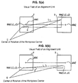
- Fig. 3(a) the center of rotation of workpiece W on workpiece carrier 4 is generally located between workpiece alignment marks WAM1 and WAM2, as is illustrated in Fig. 3(a).
- Fig. 3(a) the center of rotation of workpiece W is outside of workpiece alignment marks WAM1, WAM2, as is described below.
- distance L between the workpiece alignment marks can be measured and stored each time, it can be immediately checked whether, as a result of changes of the exposure accuracy for the arrangement of workpiece alignment marks in the prior process, major changes of the distance between the workpiece alignment marks have occurred or not. This happens when problems occur with which positioning of the mask to the workpiece cannot be performed.
- carrier control element 13 rotates workpiece carrier 4 (or mask carrier 2) by the drive of the ⁇ -carrier of the workpiece carrier 4 through the angular offset ⁇ , as in the above described conventional example.
- mask alignment marks MAM1, MAM2 and workpiece alignment marks WAM1, WAM2 are determined by means of alignment units 5.
- the X-axis carrier and Y-axis carrier of workpiece carrier 4 are driven by carrier control element 13, and workpiece carrier 4 is moved such that two alignment marks MAM1, WAM1 and MAM2, WAM2 come to rest on top of one another.
- Figs. 5(a) and (b), 6(a) and (b) and 7 are schematics of computations of the amount of position deviations in the case in which the center of rotation of workpiece W is outside of workpiece alignment marks WAM1, WAM2.
- Fig. 5(a) corresponds to the above described Fig. 4(a)
- Fig. 5(b) corresponds to Fig. 4(b).
- a case of positioning of mask M relative to workpiece W by the drive of workpiece carrier 4 was described above. However, mask carrier 2 or workpiece carrier 4 and mask carrier 2 can be driven and positioning of mask M to workpiece W can be performed.
- mask alignment mark partial illumination systems can be placed in addition; they partially illuminate the peripheral areas of mask alignment marks MAM1, MAM2, and mask alignment marks MAM1, MAM2 can be projected onto workpiece W by these partial illumination systems.
- Different modifications can be effected as means for determining mask alignment marks MAM1, MAM2 and workpiece alignment marks WAM1, WAM2.
Landscapes
- Physics & Mathematics (AREA)
- General Physics & Mathematics (AREA)
- Engineering & Computer Science (AREA)
- Multimedia (AREA)
- Exposure And Positioning Against Photoresist Photosensitive Materials (AREA)
- Exposure Of Semiconductors, Excluding Electron Or Ion Beam Exposure (AREA)
- Liquid Crystal (AREA)
- Preparing Plates And Mask In Photomechanical Process (AREA)
Applications Claiming Priority (3)
| Application Number | Priority Date | Filing Date | Title |
|---|---|---|---|
| JP203578/96 | 1996-08-01 | ||
| JP20357896A JP3324403B2 (ja) | 1996-08-01 | 1996-08-01 | マスクとワークの位置合わせ方法および装置 |
| JP20357896 | 1996-08-01 |
Publications (3)
| Publication Number | Publication Date |
|---|---|
| EP0822455A2 true EP0822455A2 (fr) | 1998-02-04 |
| EP0822455A3 EP0822455A3 (fr) | 1999-07-14 |
| EP0822455B1 EP0822455B1 (fr) | 2000-06-14 |
Family
ID=16476435
Family Applications (1)
| Application Number | Title | Priority Date | Filing Date |
|---|---|---|---|
| EP97113272A Expired - Lifetime EP0822455B1 (fr) | 1996-08-01 | 1997-07-31 | Procédé de positionnement d'un masque par rapport à une pièce à traiter et dispositif de mise en oeuvre de ce procédé |
Country Status (6)
| Country | Link |
|---|---|
| US (1) | US5923990A (fr) |
| EP (1) | EP0822455B1 (fr) |
| JP (1) | JP3324403B2 (fr) |
| KR (1) | KR100463213B1 (fr) |
| DE (1) | DE69702286T2 (fr) |
| TW (1) | TW324795B (fr) |
Cited By (1)
| Publication number | Priority date | Publication date | Assignee | Title |
|---|---|---|---|---|
| WO2008052600A1 (fr) * | 2006-04-11 | 2008-05-08 | Micronic Laser Systems Ab | Procédé et appareil d'inscription |
Families Citing this family (10)
| Publication number | Priority date | Publication date | Assignee | Title |
|---|---|---|---|---|
| US6129259A (en) * | 1997-03-31 | 2000-10-10 | Micron Technology, Inc. | Bonding and inspection system |
| JPH11233397A (ja) * | 1998-02-13 | 1999-08-27 | Mitsubishi Electric Corp | アライメント方法及び半導体装置 |
| DE19882963T1 (de) * | 1998-12-22 | 2001-05-10 | Mitsubishi Electric Corp | Positionsfehler-Messverfahren und Einrichtung unter Verwendung einer Positionsmarke und Bearbeitungseinrichtung zum Korrigieren einer Position auf Grundlage eines Ergebnisses oder eines Messpositionsfehlers unter Verwendung einer Positionsmarke |
| US7113258B2 (en) * | 2001-01-15 | 2006-09-26 | Asml Netherlands B.V. | Lithographic apparatus |
| KR100579603B1 (ko) * | 2001-01-15 | 2006-05-12 | 에이에스엠엘 네델란즈 비.브이. | 리소그래피 장치 |
| JP4208467B2 (ja) * | 2002-01-08 | 2009-01-14 | キヤノン株式会社 | カメラシステム及びその制御方法、デバイス製造装置、露光装置並びにデバイスの製造方法 |
| KR100441100B1 (ko) * | 2002-07-11 | 2004-07-19 | 엘지전자 주식회사 | 노광공정의 위치측정장치 및 위치측정방법 |
| JP4112472B2 (ja) | 2003-10-21 | 2008-07-02 | 株式会社東芝 | 半導体装置の製造方法及び半導体装置の製造装置 |
| US9547231B2 (en) * | 2013-06-12 | 2017-01-17 | Avago Technologies General Ip (Singapore) Pte. Ltd. | Device and method for making photomask assembly and photodetector device having light-collecting optical microstructure |
| CN109950191B (zh) * | 2019-03-20 | 2021-04-30 | 纳研科技(上海)有限公司 | 一种双面对准的视觉系统及对准方法 |
Family Cites Families (4)
| Publication number | Priority date | Publication date | Assignee | Title |
|---|---|---|---|---|
| US4052603A (en) * | 1974-12-23 | 1977-10-04 | International Business Machines Corporation | Object positioning process and apparatus |
| US4573791A (en) * | 1979-04-03 | 1986-03-04 | Optimetrix Corporation | Step-and-repeat projection alignment and exposure system |
| TW417158B (en) * | 1994-11-29 | 2001-01-01 | Ushio Electric Inc | Method and device for positioning mask and workpiece |
| US5841520A (en) * | 1995-08-09 | 1998-11-24 | Nikon Corporatioin | Exposure apparatus and method that use mark patterns to determine image formation characteristics of the apparatus prior to exposure |
-
1996
- 1996-08-01 JP JP20357896A patent/JP3324403B2/ja not_active Expired - Fee Related
-
1997
- 1997-06-17 TW TW086108452A patent/TW324795B/zh not_active IP Right Cessation
- 1997-07-31 DE DE69702286T patent/DE69702286T2/de not_active Expired - Lifetime
- 1997-07-31 KR KR1019970036728A patent/KR100463213B1/ko not_active Expired - Fee Related
- 1997-07-31 EP EP97113272A patent/EP0822455B1/fr not_active Expired - Lifetime
- 1997-08-01 US US08/904,768 patent/US5923990A/en not_active Expired - Lifetime
Cited By (2)
| Publication number | Priority date | Publication date | Assignee | Title |
|---|---|---|---|---|
| WO2008052600A1 (fr) * | 2006-04-11 | 2008-05-08 | Micronic Laser Systems Ab | Procédé et appareil d'inscription |
| US7525671B2 (en) | 2006-04-11 | 2009-04-28 | Micronic Laser Systems Ab | Registration method and apparatus therefor |
Also Published As
| Publication number | Publication date |
|---|---|
| JP3324403B2 (ja) | 2002-09-17 |
| DE69702286T2 (de) | 2000-12-21 |
| DE69702286D1 (de) | 2000-07-20 |
| KR100463213B1 (ko) | 2005-09-30 |
| US5923990A (en) | 1999-07-13 |
| KR19980018275A (ko) | 1998-06-05 |
| EP0822455A3 (fr) | 1999-07-14 |
| TW324795B (en) | 1998-01-11 |
| JPH1048846A (ja) | 1998-02-20 |
| EP0822455B1 (fr) | 2000-06-14 |
Similar Documents
| Publication | Publication Date | Title |
|---|---|---|
| US5881165A (en) | Process for the positioning of a mask relative to a workpiece and device for executing the process | |
| EP0920053B1 (fr) | Dispositif d'exposition de la partie périphérique d'un substrat semiconducteur | |
| EP0822455B1 (fr) | Procédé de positionnement d'un masque par rapport à une pièce à traiter et dispositif de mise en oeuvre de ce procédé | |
| US5737441A (en) | Aligning method and apparatus | |
| US5440397A (en) | Apparatus and method for exposure | |
| US5640243A (en) | Position detection method | |
| JP3466893B2 (ja) | 位置合わせ装置及びそれを用いた投影露光装置 | |
| JPH1050604A (ja) | 位置管理方法及び位置合わせ方法 | |
| WO2007018029A1 (fr) | Dispositif d’exposition et objet à exposer | |
| JPH11274027A (ja) | ステージ装置の特性計測方法及び該方法を使用する露光装置 | |
| JP3152133B2 (ja) | マスクとワークの位置合わせ方法および装置 | |
| JP2646417B2 (ja) | 露光装置 | |
| JPH08339959A (ja) | 位置合わせ方法 | |
| JP3246300B2 (ja) | マスクとワークの自動位置合わせ方法および装置 | |
| JPH1048845A (ja) | マスクとワークステージの位置合わせ方法および装置 | |
| JPS59161815A (ja) | 投影露光装置 | |
| JPH01228130A (ja) | 投影露光方法およびその装置 | |
| JP3413947B2 (ja) | 周辺露光装置 | |
| JPH08124836A (ja) | マスクとワークの位置合わせ方法および装置 | |
| JP3106920B2 (ja) | マスクパターンとワーク直線部の位置合わせ装置 | |
| JP2882821B2 (ja) | アライメント装置 | |
| JPH05283312A (ja) | 位置合わせ装置 | |
| EP1347340A2 (fr) | Dispositif d'exposition | |
| JP5166681B2 (ja) | ステップ式近接露光装置 | |
| JPH1022218A (ja) | 基板のアライメント方法 |
Legal Events
| Date | Code | Title | Description |
|---|---|---|---|
| PUAI | Public reference made under article 153(3) epc to a published international application that has entered the european phase |
Free format text: ORIGINAL CODE: 0009012 |
|
| AK | Designated contracting states |
Kind code of ref document: A2 Designated state(s): DE FR GB IT NL |
|
| PUAL | Search report despatched |
Free format text: ORIGINAL CODE: 0009013 |
|
| AK | Designated contracting states |
Kind code of ref document: A3 Designated state(s): AT BE CH DE DK ES FI FR GB GR IE IT LI LU MC NL PT SE |
|
| 17P | Request for examination filed |
Effective date: 19990625 |
|
| GRAG | Despatch of communication of intention to grant |
Free format text: ORIGINAL CODE: EPIDOS AGRA |
|
| 17Q | First examination report despatched |
Effective date: 19991006 |
|
| GRAG | Despatch of communication of intention to grant |
Free format text: ORIGINAL CODE: EPIDOS AGRA |
|
| GRAH | Despatch of communication of intention to grant a patent |
Free format text: ORIGINAL CODE: EPIDOS IGRA |
|
| GRAH | Despatch of communication of intention to grant a patent |
Free format text: ORIGINAL CODE: EPIDOS IGRA |
|
| AKX | Designation fees paid |
Free format text: DE FR GB IT NL |
|
| GRAA | (expected) grant |
Free format text: ORIGINAL CODE: 0009210 |
|
| AK | Designated contracting states |
Kind code of ref document: B1 Designated state(s): DE FR GB IT NL |
|
| REF | Corresponds to: |
Ref document number: 69702286 Country of ref document: DE Date of ref document: 20000720 |
|
| ITF | It: translation for a ep patent filed | ||
| ET | Fr: translation filed | ||
| PLBE | No opposition filed within time limit |
Free format text: ORIGINAL CODE: 0009261 |
|
| STAA | Information on the status of an ep patent application or granted ep patent |
Free format text: STATUS: NO OPPOSITION FILED WITHIN TIME LIMIT |
|
| 26N | No opposition filed | ||
| REG | Reference to a national code |
Ref country code: GB Ref legal event code: IF02 |
|
| PGFP | Annual fee paid to national office [announced via postgrant information from national office to epo] |
Ref country code: FR Payment date: 20110727 Year of fee payment: 15 |
|
| PGFP | Annual fee paid to national office [announced via postgrant information from national office to epo] |
Ref country code: DE Payment date: 20110727 Year of fee payment: 15 Ref country code: GB Payment date: 20110727 Year of fee payment: 15 |
|
| PGFP | Annual fee paid to national office [announced via postgrant information from national office to epo] |
Ref country code: NL Payment date: 20110721 Year of fee payment: 15 Ref country code: IT Payment date: 20110725 Year of fee payment: 15 |
|
| REG | Reference to a national code |
Ref country code: NL Ref legal event code: V1 Effective date: 20130201 |
|
| GBPC | Gb: european patent ceased through non-payment of renewal fee |
Effective date: 20120731 |
|
| REG | Reference to a national code |
Ref country code: FR Ref legal event code: ST Effective date: 20130329 |
|
| PG25 | Lapsed in a contracting state [announced via postgrant information from national office to epo] |
Ref country code: DE Free format text: LAPSE BECAUSE OF NON-PAYMENT OF DUE FEES Effective date: 20130201 Ref country code: GB Free format text: LAPSE BECAUSE OF NON-PAYMENT OF DUE FEES Effective date: 20120731 Ref country code: FR Free format text: LAPSE BECAUSE OF NON-PAYMENT OF DUE FEES Effective date: 20120731 Ref country code: NL Free format text: LAPSE BECAUSE OF NON-PAYMENT OF DUE FEES Effective date: 20130201 |
|
| PG25 | Lapsed in a contracting state [announced via postgrant information from national office to epo] |
Ref country code: IT Free format text: LAPSE BECAUSE OF NON-PAYMENT OF DUE FEES Effective date: 20120731 |
|
| REG | Reference to a national code |
Ref country code: DE Ref legal event code: R119 Ref document number: 69702286 Country of ref document: DE Effective date: 20130201 |