EP0822582A2 - Verfahren zur Behandlung der Oberfläche von halbleitenden Substraten - Google Patents
Verfahren zur Behandlung der Oberfläche von halbleitenden Substraten Download PDFInfo
- Publication number
- EP0822582A2 EP0822582A2 EP97305642A EP97305642A EP0822582A2 EP 0822582 A2 EP0822582 A2 EP 0822582A2 EP 97305642 A EP97305642 A EP 97305642A EP 97305642 A EP97305642 A EP 97305642A EP 0822582 A2 EP0822582 A2 EP 0822582A2
- Authority
- EP
- European Patent Office
- Prior art keywords
- deposition
- etching
- etch
- gas
- rate
- Prior art date
- Legal status (The legal status is an assumption and is not a legal conclusion. Google has not performed a legal analysis and makes no representation as to the accuracy of the status listed.)
- Granted
Links
Images


Classifications
-
- H—ELECTRICITY
- H10—SEMICONDUCTOR DEVICES; ELECTRIC SOLID-STATE DEVICES NOT OTHERWISE PROVIDED FOR
- H10P—GENERIC PROCESSES OR APPARATUS FOR THE MANUFACTURE OR TREATMENT OF DEVICES COVERED BY CLASS H10
- H10P50/00—Etching of wafers, substrates or parts of devices
- H10P50/20—Dry etching; Plasma etching; Reactive-ion etching
- H10P50/24—Dry etching; Plasma etching; Reactive-ion etching of semiconductor materials
- H10P50/242—Dry etching; Plasma etching; Reactive-ion etching of semiconductor materials of Group IV materials
- H10P50/244—Dry etching; Plasma etching; Reactive-ion etching of semiconductor materials of Group IV materials comprising alternated and repeated etching and passivation steps
Definitions
- This invention relates to methods for treatment for semiconductor substrates and in particular, but not exclusively, to methods of depositing a sidewall passivation layer on etched features and methods of etching such features including the passivation method.
- the method of this invention addresses or reduces these various problems.
- the invention consists in a method of etching a trench in a semiconductor substrate in a reactor chamber using alternately reactive ion etching and depositing a passivation layer by chemical vapour deposition, wherein one or more of the following parameters: gas flow rates, chamber pressure, plasma power, substrate bias etc rate, deposition rate, cycle time and etching/deposition ratio vary with time. The variation may be periodic.
- the etching and deposition steps may overlap and etching and deposition gases may be mixed.
- the method may include pumping out the chamber between the etching and deposition and/or between deposition and etching, in which case the pump may continue until Ppa Ppa + Ppb ⁇ x
- the etching and deposition gas flows may be continuously or abruptly variable.
- the deposition and etching gases may be supplied so that their flow rates are sinusoidal and out of phase.
- the amplitude of any of these parameters may be variable within cycles and as between cycles.
- the deposition rate is enhanced and/or etch is reduced during at least the first cycle and in appropriate circumstances in the first few cycles for example in the second to fourth cycles.
- the etch rate may be reduced by one or more of the following
- the deposition rate may be enhanced by one or more of the following
- the etch and/or deposition steps may have periods of less than 7.5 seconds or even 5 seconds to reduce surface roughness;
- the etch gas may be CF x or XeF 2 and may include one or more high atomic mass halides to reduce spontaneous etch;
- the chamber pressure may be reduced and/or the flow rate increased during deposition particularly for shallow high aspect ratio etching where it may be accompanied by increased self bias (e.g. voltage >20eV or indeed >100eV).
- the deposition step may use a hydrocarbon deposition gas to deposit a carbon or hydrocarbon layer.
- the gas may include O, N or F elements and the deposited layer may be Nitrogen or Flourine doped.
- the substrate may rest freely on a support in the chamber when back cooling would be an issue.
- the substrate may be clamped and its temperature may be controlled, to lie, for example, in the range -100°c to 100°c.
- the temperature of the chamber can also advantageously be controlled to the same temperature range as the wafer to reduce condensation on to the chamber or its furniture to reduce base roughness.
- the substrate may be GaAs, GaP, GaN, GaSo, SiGe, Mo, W or Ta and in this case the etch gas may particularly preferably be one or a combination of Cl 2 , BCl 3 SiCl 4 , SiCl 2 H 2 CH x Cl y , C x Cl y , or CH x with or without H or an inert gas. Cl 2 is particularly preferred.
- the deposition gas may be one or a combination of CH x , CH x Cl y , or C x Cl y , with or without H, or an inert gas CH 4 or CH 2 Cl 2 are particularly preferred.
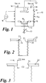
- FIG 1 illustrates schematically a prior art reactor chamber 10, which is suitable for use both in reactive ion etching and chemical vapour deposition.
- a vacuum chamber 11 incorporates a support electrode 12 for receiving a semiconductor wafer 13 and a further spaced electrode 14.
- the wafer 13 is pressed against the support 12 by a clamp 15 and is usually cooled, by backside cooling means (not shown).
- the chamber 11 is surrounded by a coil 15a and fed by a RF source 16 which is used to induce a plasma in the chamber 11 between the electrodes 12 and 14.
- a microwave power supply may be used to create the plasma.
- a plasma bias which can be either RF or DC and can be connected to the support electrode 12 so as to influence the passage of ions from the plasma down on to the wafer 13.
- An example of such an adjustable bias means is indicated at 17.
- the chamber is provided with a gas inlet port 18 through which deposition or etched gases can be introduced and an exhaust port 19 for the removal of gaseous process products and any excess process gas. The operation of such a reactor in either the RIE or CVD modes is well understood in the art.
- the Applicant proposes a series of improvements to such processes to enable the formation of more smooth walled formations and particularly better quality deep and/or high aspect ratio formations. For convenience the description will therefore be divided into sections.
- these films or layers are also desirably deposited at high self biases eg. 20eV upwards and preferably over 100 eV, there is an additional significant advantage when it comes to high aspect ratio formations, because the high self-bias ensures that the transport of the depositing material down to the base of the formation being etched is enhanced to prevent re-entrant sidewall etching.
- This transportation effect can also be improved by progressively reducing the chamber pressure and/or increasing the gas flow rate, so as to reduce the residence time.
- the feature opening size (or critical dimension) can be in the ⁇ 0.5 ⁇ m range.
- hydrocarbon (H-C) films formed by this passivation have significant advantages over the prior art fluorocarbon films.
- the H-C films can for example be readily removed after etching processing has been completed by dry ashing (oxygen plasma) treatment. This can be particularly important in he formation of MEMS (micro-electro-mechanical systems) where wet processing can result in sticking of resonant structures which are separated by high aspect trenches. In other applications, eg. optical or biomedical devices, it can be essential to remove completely the side wall layer.
- dry ashing oxygen plasma
- the H-C films may be deposited from a wide range of H-C precursors (eg. CH 4 , C 2 H 4 , C 3 H 6 , C 4 H 8 , C 2 H 2 . etc. including high molecular weight aromatic H-C's). These may be mixed with noble gases and/or H 2 .
- An oxygen source gas can also be added (eg CO, CO 2 , O 2 etc.) can be used to control the phase balance of the film during deposition. The oxygen will tend to remove the graphitic phase (sp 2 ) of the carbon leaving the harder (sp 3 ) phase. Thus, the proportion of oxygen present will affect the characteristics o the film or layer, which is finally deposited.
- H 2 can be mixed in with the H-C precursor.
- H 2 will preferentially etch silicon and if the proportions are correctly selected, it is possible to achieve side wall passivation, whilst continuing the etching of the base of the hole during passivation phase.
- the preferred procedure for this is to mix the selected H-C precursor (eg. CH 4 ) with H 2 and process a mask patterned silicon surface with the mixture in the apparatus, which is to be used for the proposed etch procedure.
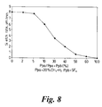
- the silicon etch rate is plotted as a function of CH 4 concentration in H 2 and an example of such a plot is shown in Figure 4. It will be noted that the etch rate increases from an initial steady state with increasing percentage of CH 4 to a peak before decreasing to zero.
- the graph illustrates the following mechanisms taking place.
- the etch is essentially dominated by the action of H 2 to form SiHx reaction products.
- the CH 4 etching of the substrate becomes significant (by forming Si(CHx)y products) and the etch rate increases.
- Deposition of a hydrocarbon layer is taking place throughout although due to the etching there is no net deposition on this part of the graph.
- the deposition begins to dominate the etching process until at around 38% for CH 4 , net deposition occurs.
- the layer or coating laid down is relatively hard because the reduced graphitic phase and the process can be operated in the rising portion of the etch rate graph, because the coating is much more resistant to etching, than the silicon substrate. It is thus possible to etch the silicon throughout the deposition phase. Selectivies exceeding 100:1 to mask or resist are readily achieved. It should particularly be noted that, whilst there is a significant removal of the graphitic phase due to ion bombardment of the mask 22, the high directionality of the ions means that the side wall coating is relatively untouched.
- the process can also be operated at low mean ion energies either with a H-C precursor alone or with H 2 dilution. In that latter case it is preferred that the process is operated in the descending part of the etch graph. ie. for CH 4 at a percentage >18% but ⁇ 38% when net deposition occurs. Typically the range for CH 4 would be 18% to 30%.
- Figure 5 illustrates the step coverage (side wall deposition measured at 50% of the step height versus surface deposition) for H-C films using CH 4 and H 2 under a range of conditions including the two embodiments described above.
- Figure 5 shows that high ion energies increase the step coverage, but even with low bias conditions, there is sufficient passivation to protect against lateral etching. Further, in this latter case the higher deposition rate serves further to enhance the mask selectivity.
- the deposition rate at low ion energies is a factor of two greater over the 100ev case.
- Figure 6 illustrates how various parameters of the process may be synchronised.
- 6d shows continuous and unchanging coil power, whilst at 6e the coil power is switched to enhance the etch or deposition step and the power during etch may be different to that selected for deposition depending on the process performance required.
- 6e illustrates a higher coil power during deposition.
- 6f to i show similar variations in bias power.
- 6f has a high bias power during etch to allow ease of removal of he passivation film, whilst 6g illustrates the use of an initial higher power pulse to enhance this removal process, whilst maintaining the mean ion energy lower, with resultant selectivity benefits.
- 6h is a combination of 6f and 6g for when the higher ion energies are required during etching (eg. with deep trenches). 6i simply shows that bias may be off during deposition.
- the acceptable segregation period of the gases is determined by the residual partial pressure of gas A (Ppa) which can be tolerated in the partial pressure of gas B(Ppb).
- Ppa residual partial pressure of gas A
- Ppb residual partial pressure of gas B(Ppb)
- This minimum value of Ppa in Ppb is established from the characteristic process rate (etch or deposition) as a function of Ppa/(Ppa + Ppb).
- 4985114 propose switching off or reducing deposition gas flow for a long period before the plasma is switched on. This can mean that the plasma power is on only for a small portion of the total cycle times leading to a significant reduction in etch rate.
- the Applicants propose that the chamber should be pumped out between at least some of the gas changeovers, but care must be taken to maintain pressure and gas flow stabilisation.
- Typical process parameters are as follows: 1. Deposition step CH 4 step time 2-15 seconds ; 4-6 seconds preferred H 2 step time 2-15 seconds ; 4-6 seconds preferred Coil rf power 600W-1kW ; 800W preferred Bias rf power High mean in energy case: 500W-300W-100W preferred Low mean in energy case: 0W-30W-10W preferred Pressure 2 mTorr-50 mTorr; 20 mTorr preferred 2.
- the sidewall roughness is essentially a manifestation of the enhanced lateral etch component, it can be reduced by limiting this component of the etch.
- the desired effect can be obtained in one of a number of ways: partially mixing the passivation and etch steps (overlapping) ; minimising the etch (and hence corresponding passivation) duration; reducing the etch product volatility by reducing the wafer temperature; adding passivation component to the etch gas e.g. SF 6 with added 0, N, C, CF x , CH x , or replacing the etch gas with one of lower reactive species liberating gas such as SF 6 replaced by CF x etc.
- the Applicant has also appreciated that changes in the levels of etching and deposition are desirable at different stages within the process.
- the system can be tuned in an appropriate manner to achieve good anisotropic etching with proper sidewall passivation.
- the sidewall notching' problem is particularly sensitive to the exposed silicon area (worse at low exposed areas ⁇ 30%) and is also correspondingly worse at high silicon mean etch rates.
- the Applicants believe such notching to be caused by a relatively high concentration of etch species, during the initial etch/deposition cycles. Therefore the solutions adopted by the Applicants are to either enhance the passivation or quench etch species during the first cycles. The latter can be achieved either by process adjustment (ramping one of more of the parameters) or by placing a material within the reactor which will consume (by chemical reaction) the etch species, such as Si, Ti, W etc. reacting with the F etchant. Such chemical loading has the drawback of reducing the mean etch rate, as the quenching is only necessary for the first few etch steps. Thus, process adjustment solutions are considered superior.
- the notched sidewall can be modified. If abrupt steps are used to vary the process parameters, abrupt transitions are produced in the sidewall profiles.
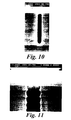
- the SEMs in Figures 12 and 13 illustrate this for different process parameters.
- the transition in the process parameters is clearly marked as an abrupt transition in the sidewall profile at the point of parameter change (after 8.5 ⁇ m etch depth). (Note that the sidewall notches have been eliminated.)
- Figure 13 illustrates yet another process parameter abrupt/step change.
- the sidewall passivation is high enough to result in a positive profile (and no notching) for the first 2 ⁇ m. When the reduced passivation conditions are applied, it is characterised by the transition in sidewall angle and reappearance of the notching.
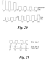
- Figure 20 illustrates a synchronisation between deposition and etch gases which have been used for the initial cycles to reduce side wall notching. Typical operating conditions are given in Figure 19a and its associated SEM in Figure 14.
- Figure 21 illustrates a synchronisation reference to using a scavenger gas with method (a) of side wall notch reduction technique. The dotted line indicates the alternative of the scavenger gas flow rate being decreasingly ramped.
- Figure 9i shows a synchronisation for achieving a deep high aspect ratio anisotropic etch although the ramping technique shown can also be used for side wall notch reduction.
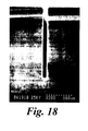
- the conditions of Figure 19b can be used to achieve the results shown in Figure 18.
- the degree of sidewall roughness can also alternatively be reduced by limiting the cycle times. For example it has been discovered that it is desirable to limit the etch and deposition periods to less than 7.5 seconds and preferably less than 5 seconds.
Landscapes
- Drying Of Semiconductors (AREA)
- Physical Deposition Of Substances That Are Components Of Semiconductor Devices (AREA)
- Weting (AREA)
- Mechanical Treatment Of Semiconductor (AREA)
Priority Applications (1)
| Application Number | Priority Date | Filing Date | Title |
|---|---|---|---|
| EP03013020A EP1357584A3 (de) | 1996-08-01 | 1997-07-28 | Verfahren zur Oberflachensbehandlung von halbleitenden Substraten |
Applications Claiming Priority (4)
| Application Number | Priority Date | Filing Date | Title |
|---|---|---|---|
| GBGB9616224.3A GB9616224D0 (en) | 1996-08-01 | 1996-08-01 | Method of surface treatment of semiconductor substrates |
| GB9616224 | 1996-08-01 | ||
| GB9616223 | 1996-08-01 | ||
| GBGB9616223.5A GB9616223D0 (en) | 1996-08-01 | 1996-08-01 | Method of surface treatment of semiconductor substrates |
Related Child Applications (2)
| Application Number | Title | Priority Date | Filing Date |
|---|---|---|---|
| EP03013020A Division EP1357584A3 (de) | 1996-08-01 | 1997-07-28 | Verfahren zur Oberflachensbehandlung von halbleitenden Substraten |
| EP02019429 Division | 2002-08-30 |
Publications (3)
| Publication Number | Publication Date |
|---|---|
| EP0822582A2 true EP0822582A2 (de) | 1998-02-04 |
| EP0822582A3 EP0822582A3 (de) | 1998-05-13 |
| EP0822582B1 EP0822582B1 (de) | 2003-10-01 |
Family
ID=26309796
Family Applications (2)
| Application Number | Title | Priority Date | Filing Date |
|---|---|---|---|
| EP03013020A Withdrawn EP1357584A3 (de) | 1996-08-01 | 1997-07-28 | Verfahren zur Oberflachensbehandlung von halbleitenden Substraten |
| EP97305642A Expired - Lifetime EP0822582B1 (de) | 1996-08-01 | 1997-07-28 | Verfahren zur Ätzung von Substraten |
Family Applications Before (1)
| Application Number | Title | Priority Date | Filing Date |
|---|---|---|---|
| EP03013020A Withdrawn EP1357584A3 (de) | 1996-08-01 | 1997-07-28 | Verfahren zur Oberflachensbehandlung von halbleitenden Substraten |
Country Status (5)
| Country | Link |
|---|---|
| US (1) | US6051503A (de) |
| EP (2) | EP1357584A3 (de) |
| JP (2) | JP3540129B2 (de) |
| AT (1) | ATE251341T1 (de) |
| DE (1) | DE69725245T2 (de) |
Cited By (52)
| Publication number | Priority date | Publication date | Assignee | Title |
|---|---|---|---|---|
| WO1999010922A1 (de) * | 1997-08-21 | 1999-03-04 | Robert Bosch Gmbh | Verfahren zum anisotropen ätzen von silizium |
| WO2000024046A1 (en) | 1998-10-22 | 2000-04-27 | Tokyo Electron Limited | Plasma etching method |
| WO2000026956A1 (en) * | 1998-11-04 | 2000-05-11 | Surface Technology Systems Limited | A method and apparatus for etching a substrate |
| WO2000036631A1 (en) * | 1998-12-11 | 2000-06-22 | Surface Technology Systems Limited | Plasma processing apparatus |
| GB2348399A (en) * | 1999-03-31 | 2000-10-04 | Univ Glasgow | Reactive ion etching with control of etch gas flow rate, pressure and rf power |
| WO2000067306A1 (de) * | 1999-04-30 | 2000-11-09 | Robert Bosch Gmbh | Verfahren zum anisotropen plasmaätzen von halbleitern |
| WO2000079579A2 (de) | 1999-06-18 | 2000-12-28 | Robert Bosch Gmbh | Vorrichtung und verfahren zum hochratenätzen eines substrates mit einer plasmaätzanlage und vorrichtung und verfahren zum zünden eines plasmas und hochregeln oder pulsen der plasmaleistung |
| WO2001003181A1 (de) * | 1999-06-30 | 2001-01-11 | Infineon Technologies Ag | Ätzverfahren für kondensatorengraben |
| WO2001008207A1 (en) * | 1999-07-23 | 2001-02-01 | Surface Technology Systems Plc | Method and apparatus for anisotropic etching |
| US6290864B1 (en) | 1999-10-26 | 2001-09-18 | Reflectivity, Inc. | Fluoride gas etching of silicon with improved selectivity |
| EP1047122A3 (de) * | 1999-04-21 | 2001-12-05 | Alcatel | Verfahren zur anisotropen Ätzung von Substraten |
| US6417013B1 (en) | 1999-01-29 | 2002-07-09 | Plasma-Therm, Inc. | Morphed processing of semiconductor devices |
| US6489248B2 (en) | 1999-10-06 | 2002-12-03 | Applied Materials, Inc. | Method and apparatus for etch passivating and etching a substrate |
| EP1077475A3 (de) * | 1999-08-11 | 2003-04-02 | Applied Materials, Inc. | Verfahren zur Mikrobearbeitung einer Körperhölung mit mehrfachem Profil |
| WO2003030239A1 (en) * | 2001-09-28 | 2003-04-10 | Sumitomo Precision Products Co., Ltd. | Silicon substrate etching method and etching apparatus |
| US6555480B2 (en) | 2001-07-31 | 2003-04-29 | Hewlett-Packard Development Company, L.P. | Substrate with fluidic channel and method of manufacturing |
| WO2004017368A2 (en) | 2002-08-16 | 2004-02-26 | Unaxis Usa, Inc. | Sidewall smoothing in high aspect ratio/deep etching using a discreet gas switching method |
| EP1235263A3 (de) * | 2001-02-22 | 2004-05-19 | Texas Instruments Incorporated | Modulation der Eigenschaften eines Ätzverfahrens durch Gas-Umschaltung |
| US6749717B1 (en) * | 1997-02-04 | 2004-06-15 | Micron Technology, Inc. | Device for in-situ cleaning of an inductively-coupled plasma chambers |
| WO2004034445A3 (en) * | 2002-10-11 | 2004-08-12 | Lam Res Corp | A method for plasma etching performance enhancement |
| US6818562B2 (en) | 2002-04-19 | 2004-11-16 | Applied Materials Inc | Method and apparatus for tuning an RF matching network in a plasma enhanced semiconductor wafer processing system |
| US6833325B2 (en) | 2002-10-11 | 2004-12-21 | Lam Research Corporation | Method for plasma etching performance enhancement |
| US6849554B2 (en) | 2002-05-01 | 2005-02-01 | Applied Materials, Inc. | Method of etching a deep trench having a tapered profile in silicon |
| US6849471B2 (en) | 2003-03-28 | 2005-02-01 | Reflectivity, Inc. | Barrier layers for microelectromechanical systems |
| WO2004093162A3 (de) * | 2003-04-15 | 2005-02-24 | Univ Dresden Tech | Siliziumsubstrat mit positiven ätzprofilen mit definiertem böschungswinkel und verfahren zur herstellung |
| US6913942B2 (en) | 2003-03-28 | 2005-07-05 | Reflectvity, Inc | Sacrificial layers for use in fabrications of microelectromechanical devices |
| US6942811B2 (en) | 1999-10-26 | 2005-09-13 | Reflectivity, Inc | Method for achieving improved selectivity in an etching process |
| US6949202B1 (en) | 1999-10-26 | 2005-09-27 | Reflectivity, Inc | Apparatus and method for flow of process gas in an ultra-clean environment |
| US6960305B2 (en) | 1999-10-26 | 2005-11-01 | Reflectivity, Inc | Methods for forming and releasing microelectromechanical structures |
| US6965468B2 (en) | 2003-07-03 | 2005-11-15 | Reflectivity, Inc | Micromirror array having reduced gap between adjacent micromirrors of the micromirror array |
| US6969635B2 (en) | 2000-12-07 | 2005-11-29 | Reflectivity, Inc. | Methods for depositing, releasing and packaging micro-electromechanical devices on wafer substrates |
| WO2005122226A1 (en) * | 2004-06-03 | 2005-12-22 | Lam Research Corporation | Method for plasma stripping using periodic modulation of gas chemistry and hydrocarbon addition |
| US6980347B2 (en) | 2003-07-03 | 2005-12-27 | Reflectivity, Inc | Micromirror having reduced space between hinge and mirror plate of the micromirror |
| US7019376B2 (en) | 2000-08-11 | 2006-03-28 | Reflectivity, Inc | Micromirror array device with a small pitch size |
| US7027200B2 (en) | 2002-03-22 | 2006-04-11 | Reflectivity, Inc | Etching method used in fabrications of microstructures |
| US7041224B2 (en) | 1999-10-26 | 2006-05-09 | Reflectivity, Inc. | Method for vapor phase etching of silicon |
| US7189332B2 (en) | 2001-09-17 | 2007-03-13 | Texas Instruments Incorporated | Apparatus and method for detecting an endpoint in a vapor phase etch |
| EP1804281A1 (de) | 2005-12-28 | 2007-07-04 | STMicroelectronics S.r.l. | Verfahren zum Ätzen eines tiefen Grabens in einem halbleitenden Gegenstand, und halbleitender Gegenstand so hergestellt. |
| US7241683B2 (en) | 2005-03-08 | 2007-07-10 | Lam Research Corporation | Stabilized photoresist structure for etching process |
| WO2008028452A1 (de) * | 2006-09-06 | 2008-03-13 | Technische Universität Dresden | Verfahren zum plasmaätzen zur erzeugung positiver ätzprofile in siliziumsubstraten |
| EP1688924A3 (de) * | 2005-01-28 | 2008-03-19 | Hitachi Global Storage Technologies Netherlands B.V. | Verfahren zur Herstellung eines magnetoresistiven Sensors |
| EP1831429A4 (de) * | 2004-12-22 | 2008-10-22 | Lam Res Corp | Verfahren und vorrichtung für den sequenziellen wechsel von plasmaprozessen zur optimierung eines substrats |
| US7491647B2 (en) | 2005-03-08 | 2009-02-17 | Lam Research Corporation | Etch with striation control |
| US7645704B2 (en) | 2003-09-17 | 2010-01-12 | Texas Instruments Incorporated | Methods and apparatus of etch process control in fabrications of microstructures |
| US7803536B2 (en) | 2002-09-20 | 2010-09-28 | Integrated Dna Technologies, Inc. | Methods of detecting fluorescence with anthraquinone quencher dyes |
| EP1611603A4 (de) * | 2003-04-09 | 2010-10-13 | Lam Res Corp | Plasmaätzverfahren mittels periodischer modulation von gaschemie |
| US7910489B2 (en) | 2006-02-17 | 2011-03-22 | Lam Research Corporation | Infinitely selective photoresist mask etch |
| US7977390B2 (en) | 2002-10-11 | 2011-07-12 | Lam Research Corporation | Method for plasma etching performance enhancement |
| WO2013128181A1 (en) * | 2012-02-29 | 2013-09-06 | Oxford Instruments Nanotechnology Tools Limited | Methods and apparatus for depositing and/or etching material on a substrate |
| KR20170131279A (ko) * | 2016-05-20 | 2017-11-29 | 에스피티에스 테크놀러지스 리미티드 | 워크피스를 플라즈마 에칭하기 위한 방법 |
| US10622193B2 (en) | 2014-11-25 | 2020-04-14 | Spts Technologies Limited | Plasma etching apparatus |
| CN111257596A (zh) * | 2020-02-25 | 2020-06-09 | 西南交通大学 | 一种扫描探针显微镜狭小实验腔环境气氛精确控制装置 |
Families Citing this family (177)
| Publication number | Priority date | Publication date | Assignee | Title |
|---|---|---|---|---|
| GB9616225D0 (en) * | 1996-08-01 | 1996-09-11 | Surface Tech Sys Ltd | Method of surface treatment of semiconductor substrates |
| WO1999046810A1 (en) * | 1998-03-12 | 1999-09-16 | Hitachi, Ltd. | Method for processing surface of sample |
| US6194038B1 (en) | 1998-03-20 | 2001-02-27 | Applied Materials, Inc. | Method for deposition of a conformal layer on a substrate |
| US6642149B2 (en) * | 1998-09-16 | 2003-11-04 | Tokyo Electron Limited | Plasma processing method |
| US20030015496A1 (en) * | 1999-07-22 | 2003-01-23 | Sujit Sharan | Plasma etching process |
| JP2001110784A (ja) * | 1999-10-12 | 2001-04-20 | Hitachi Ltd | プラズマ処理装置および処理方法 |
| US6890863B1 (en) * | 2000-04-27 | 2005-05-10 | Micron Technology, Inc. | Etchant and method of use |
| JP3525862B2 (ja) * | 2000-05-22 | 2004-05-10 | トヨタ自動車株式会社 | センサ素子及びセンサ装置 |
| CA2424520C (en) * | 2000-08-21 | 2007-01-02 | The Cleveland Clinic Foundation | Microneedle array module and method of fabricating the same |
| US6784108B1 (en) * | 2000-08-31 | 2004-08-31 | Micron Technology, Inc. | Gas pulsing for etch profile control |
| US6402301B1 (en) | 2000-10-27 | 2002-06-11 | Lexmark International, Inc | Ink jet printheads and methods therefor |
| WO2002075801A2 (en) * | 2000-11-07 | 2002-09-26 | Tokyo Electron Limited | Method of fabricating oxides with low defect densities |
| US6743732B1 (en) * | 2001-01-26 | 2004-06-01 | Taiwan Semiconductor Manufacturing Company | Organic low K dielectric etch with NH3 chemistry |
| US6451673B1 (en) * | 2001-02-15 | 2002-09-17 | Advanced Micro Devices, Inc. | Carrier gas modification for preservation of mask layer during plasma etching |
| US20020139477A1 (en) * | 2001-03-30 | 2002-10-03 | Lam Research Corporation | Plasma processing method and apparatus with control of plasma excitation power |
| US20020158047A1 (en) * | 2001-04-27 | 2002-10-31 | Yiqiong Wang | Formation of an optical component having smooth sidewalls |
| US20020158046A1 (en) * | 2001-04-27 | 2002-10-31 | Chi Wu | Formation of an optical component |
| US6635556B1 (en) * | 2001-05-17 | 2003-10-21 | Matrix Semiconductor, Inc. | Method of preventing autodoping |
| US6800210B2 (en) * | 2001-05-22 | 2004-10-05 | Reflectivity, Inc. | Method for making a micromechanical device by removing a sacrificial layer with multiple sequential etchants |
| US6555166B2 (en) * | 2001-06-29 | 2003-04-29 | International Business Machines | Method for reducing the microloading effect in a chemical vapor deposition reactor |
| US7067849B2 (en) | 2001-07-17 | 2006-06-27 | Lg Electronics Inc. | Diode having high brightness and method thereof |
| US6890859B1 (en) * | 2001-08-10 | 2005-05-10 | Cypress Semiconductor Corporation | Methods of forming semiconductor structures having reduced defects, and articles and devices formed thereby |
| US7115516B2 (en) * | 2001-10-09 | 2006-10-03 | Applied Materials, Inc. | Method of depositing a material layer |
| US6949395B2 (en) | 2001-10-22 | 2005-09-27 | Oriol, Inc. | Method of making diode having reflective layer |
| US7148520B2 (en) | 2001-10-26 | 2006-12-12 | Lg Electronics Inc. | Diode having vertical structure and method of manufacturing the same |
| US6906845B2 (en) * | 2001-11-26 | 2005-06-14 | Samsung Electronics Co., Ltd. | Micro-mechanical device having anti-stiction layer and method of manufacturing the device |
| FR2834382B1 (fr) * | 2002-01-03 | 2005-03-18 | Cit Alcatel | Procede et dispositif de gravure anisotrope du silicium a haut facteur d'aspect |
| US6979652B2 (en) * | 2002-04-08 | 2005-12-27 | Applied Materials, Inc. | Etching multi-shaped openings in silicon |
| US6846746B2 (en) * | 2002-05-01 | 2005-01-25 | Applied Materials, Inc. | Method of smoothing a trench sidewall after a deep trench silicon etch process |
| US6759340B2 (en) | 2002-05-09 | 2004-07-06 | Padmapani C. Nallan | Method of etching a trench in a silicon-on-insulator (SOI) structure |
| US6905626B2 (en) * | 2002-07-24 | 2005-06-14 | Unaxis Usa Inc. | Notch-free etching of high aspect SOI structures using alternating deposition and etching and pulsed plasma |
| US7074723B2 (en) * | 2002-08-02 | 2006-07-11 | Applied Materials, Inc. | Method of plasma etching a deeply recessed feature in a substrate using a plasma source gas modulated etchant system |
| US6946362B2 (en) * | 2002-09-06 | 2005-09-20 | Hewlett-Packard Development Company, L.P. | Method and apparatus for forming high surface area material films and membranes |
| US6921490B1 (en) | 2002-09-06 | 2005-07-26 | Kotura, Inc. | Optical component having waveguides extending from a common region |
| US6902867B2 (en) * | 2002-10-02 | 2005-06-07 | Lexmark International, Inc. | Ink jet printheads and methods therefor |
| DE10247913A1 (de) * | 2002-10-14 | 2004-04-22 | Robert Bosch Gmbh | Plasmaanlage und Verfahren zum anisotropen Einätzen von Strukturen in ein Substrat |
| US7115520B2 (en) * | 2003-04-07 | 2006-10-03 | Unaxis Usa, Inc. | Method and apparatus for process control in time division multiplexed (TDM) etch process |
| US20040224524A1 (en) * | 2003-05-09 | 2004-11-11 | Applied Materials, Inc. | Maintaining the dimensions of features being etched on a lithographic mask |
| JP4161857B2 (ja) * | 2003-09-10 | 2008-10-08 | 株式会社デンソー | 半導体装置の製造方法 |
| US7135410B2 (en) * | 2003-09-26 | 2006-11-14 | Lam Research Corporation | Etch with ramping |
| US20050112891A1 (en) * | 2003-10-21 | 2005-05-26 | David Johnson | Notch-free etching of high aspect SOI structures using a time division multiplex process and RF bias modulation |
| USRE42955E1 (en) * | 2003-12-04 | 2011-11-22 | Bae Systems Information And Electronic Systems Integration Inc. | GaN-based permeable base transistor and method of fabrication |
| JP3816484B2 (ja) | 2003-12-15 | 2006-08-30 | 日本航空電子工業株式会社 | ドライエッチング方法 |
| US20050211668A1 (en) * | 2004-03-26 | 2005-09-29 | Lam Research Corporation | Methods of processing a substrate with minimal scalloping |
| JP4416569B2 (ja) * | 2004-05-24 | 2010-02-17 | キヤノン株式会社 | 堆積膜形成方法および堆積膜形成装置 |
| US7053003B2 (en) * | 2004-10-27 | 2006-05-30 | Lam Research Corporation | Photoresist conditioning with hydrogen ramping |
| JP2006173293A (ja) * | 2004-12-15 | 2006-06-29 | Toshiba Corp | 半導体装置の製造方法 |
| US20070026682A1 (en) * | 2005-02-10 | 2007-02-01 | Hochberg Michael J | Method for advanced time-multiplexed etching |
| GB0508706D0 (en) | 2005-04-28 | 2005-06-08 | Oxford Instr Plasma Technology | Method of generating and using a plasma processing control program |
| FR2887073B1 (fr) * | 2005-06-14 | 2007-08-10 | Alcatel Sa | Procede de pilotage de la pression dans une chambre de procede |
| US7425507B2 (en) * | 2005-06-28 | 2008-09-16 | Micron Technology, Inc. | Semiconductor substrates including vias of nonuniform cross section, methods of forming and associated structures |
| JP4707178B2 (ja) * | 2005-06-29 | 2011-06-22 | キヤノンマーケティングジャパン株式会社 | エッチング方法およびエッチング装置 |
| US7341953B2 (en) * | 2006-04-17 | 2008-03-11 | Lam Research Corporation | Mask profile control for controlling feature profile |
| US7829465B2 (en) * | 2006-08-09 | 2010-11-09 | Shouliang Lai | Method for plasma etching of positively sloped structures |
| US7309646B1 (en) * | 2006-10-10 | 2007-12-18 | Lam Research Corporation | De-fluoridation process |
| JP2008205436A (ja) * | 2007-01-26 | 2008-09-04 | Toshiba Corp | 微細構造体の製造方法 |
| US20080239428A1 (en) * | 2007-04-02 | 2008-10-02 | Inphase Technologies, Inc. | Non-ft plane angular filters |
| US20080284835A1 (en) * | 2007-05-15 | 2008-11-20 | Panchawagh Hrishikesh V | Integral, micromachined gutter for inkjet printhead |
| US7758155B2 (en) * | 2007-05-15 | 2010-07-20 | Eastman Kodak Company | Monolithic printhead with multiple rows of inkjet orifices |
| US9123509B2 (en) * | 2007-06-29 | 2015-09-01 | Varian Semiconductor Equipment Associates, Inc. | Techniques for plasma processing a substrate |
| US20090033727A1 (en) * | 2007-07-31 | 2009-02-05 | Anagnostopoulos Constantine N | Lateral flow device printhead with internal gutter |
| US8609546B2 (en) | 2007-11-29 | 2013-12-17 | Lam Research Corporation | Pulsed bias plasma process to control microloading |
| US9059116B2 (en) | 2007-11-29 | 2015-06-16 | Lam Research Corporation | Etch with pulsed bias |
| JP5172417B2 (ja) * | 2008-03-27 | 2013-03-27 | Sppテクノロジーズ株式会社 | シリコン構造体の製造方法及びその製造装置並びにその製造プログラム |
| US8585179B2 (en) * | 2008-03-28 | 2013-11-19 | Eastman Kodak Company | Fluid flow in microfluidic devices |
| JP5308080B2 (ja) * | 2008-06-18 | 2013-10-09 | Sppテクノロジーズ株式会社 | シリコン構造体の製造方法及びその製造装置並びにその製造プログラム |
| US8338308B2 (en) * | 2008-12-19 | 2012-12-25 | The Board Of Trustees Of The University Of Illinois | Method of plasma etching Ga-based compound semiconductors |
| WO2010088267A2 (en) * | 2009-01-31 | 2010-08-05 | Applied Materials, Inc. | Method and apparatus for etching |
| JP5532394B2 (ja) * | 2009-10-15 | 2014-06-25 | セイコーエプソン株式会社 | 半導体装置及び回路基板並びに電子機器 |
| CN102135733B (zh) * | 2010-01-27 | 2012-12-05 | 中芯国际集成电路制造(上海)有限公司 | 光阻去除方法 |
| US8384183B2 (en) * | 2010-02-19 | 2013-02-26 | Allegro Microsystems, Inc. | Integrated hall effect element having a germanium hall plate |
| JP5223878B2 (ja) | 2010-03-30 | 2013-06-26 | 株式会社デンソー | 半導体装置の製造方法 |
| US8642448B2 (en) | 2010-06-22 | 2014-02-04 | Applied Materials, Inc. | Wafer dicing using femtosecond-based laser and plasma etch |
| KR20120000612A (ko) * | 2010-06-28 | 2012-01-04 | 삼성전자주식회사 | 반도체 장치의 제조 방법 |
| US8133349B1 (en) | 2010-11-03 | 2012-03-13 | Lam Research Corporation | Rapid and uniform gas switching for a plasma etch process |
| US8802545B2 (en) | 2011-03-14 | 2014-08-12 | Plasma-Therm Llc | Method and apparatus for plasma dicing a semi-conductor wafer |
| US9070760B2 (en) | 2011-03-14 | 2015-06-30 | Plasma-Therm Llc | Method and apparatus for plasma dicing a semi-conductor wafer |
| US8440473B2 (en) | 2011-06-06 | 2013-05-14 | Lam Research Corporation | Use of spectrum to synchronize RF switching with gas switching during etch |
| US8609548B2 (en) * | 2011-06-06 | 2013-12-17 | Lam Research Corporation | Method for providing high etch rate |
| US9029242B2 (en) | 2011-06-15 | 2015-05-12 | Applied Materials, Inc. | Damage isolation by shaped beam delivery in laser scribing process |
| US9129904B2 (en) | 2011-06-15 | 2015-09-08 | Applied Materials, Inc. | Wafer dicing using pulse train laser with multiple-pulse bursts and plasma etch |
| US8598016B2 (en) * | 2011-06-15 | 2013-12-03 | Applied Materials, Inc. | In-situ deposited mask layer for device singulation by laser scribing and plasma etch |
| US8703581B2 (en) | 2011-06-15 | 2014-04-22 | Applied Materials, Inc. | Water soluble mask for substrate dicing by laser and plasma etch |
| US8912077B2 (en) | 2011-06-15 | 2014-12-16 | Applied Materials, Inc. | Hybrid laser and plasma etch wafer dicing using substrate carrier |
| US8557683B2 (en) | 2011-06-15 | 2013-10-15 | Applied Materials, Inc. | Multi-step and asymmetrically shaped laser beam scribing |
| US8759197B2 (en) | 2011-06-15 | 2014-06-24 | Applied Materials, Inc. | Multi-step and asymmetrically shaped laser beam scribing |
| US8507363B2 (en) * | 2011-06-15 | 2013-08-13 | Applied Materials, Inc. | Laser and plasma etch wafer dicing using water-soluble die attach film |
| JP5981106B2 (ja) * | 2011-07-12 | 2016-08-31 | 東京エレクトロン株式会社 | プラズマエッチング方法 |
| US9046690B2 (en) | 2011-10-20 | 2015-06-02 | Si-Ware Systems | Integrated monolithic optical bench containing 3-D curved optical elements and methods of its fabrication |
| CN102431960A (zh) * | 2011-12-07 | 2012-05-02 | 华中科技大学 | 一种硅通孔刻蚀方法 |
| CN103159163B (zh) * | 2011-12-19 | 2016-06-08 | 北京北方微电子基地设备工艺研究中心有限责任公司 | 基片刻蚀方法及基片处理设备 |
| US8946057B2 (en) | 2012-04-24 | 2015-02-03 | Applied Materials, Inc. | Laser and plasma etch wafer dicing using UV-curable adhesive film |
| JP5713043B2 (ja) | 2012-05-07 | 2015-05-07 | 株式会社デンソー | 半導体基板の製造方法 |
| US9048309B2 (en) | 2012-07-10 | 2015-06-02 | Applied Materials, Inc. | Uniform masking for wafer dicing using laser and plasma etch |
| US8859397B2 (en) | 2012-07-13 | 2014-10-14 | Applied Materials, Inc. | Method of coating water soluble mask for laser scribing and plasma etch |
| US8940619B2 (en) | 2012-07-13 | 2015-01-27 | Applied Materials, Inc. | Method of diced wafer transportation |
| CN102832096B (zh) * | 2012-09-20 | 2015-11-25 | 中微半导体设备(上海)有限公司 | 一种用于真空处理装置的气体供应装置及其气体供应及切换方法 |
| US9252057B2 (en) | 2012-10-17 | 2016-02-02 | Applied Materials, Inc. | Laser and plasma etch wafer dicing with partial pre-curing of UV release dicing tape for film frame wafer application |
| US8975162B2 (en) | 2012-12-20 | 2015-03-10 | Applied Materials, Inc. | Wafer dicing from wafer backside |
| US9236305B2 (en) | 2013-01-25 | 2016-01-12 | Applied Materials, Inc. | Wafer dicing with etch chamber shield ring for film frame wafer applications |
| US9018108B2 (en) | 2013-01-25 | 2015-04-28 | Applied Materials, Inc. | Low shrinkage dielectric films |
| TWI619165B (zh) | 2013-03-14 | 2018-03-21 | 應用材料股份有限公司 | 以雷射及電漿蝕刻進行的基板切割所用的含非光可界定雷射能量吸收層的多層遮罩 |
| JP6180824B2 (ja) * | 2013-07-02 | 2017-08-16 | 東京エレクトロン株式会社 | プラズマエッチング方法及びプラズマエッチング装置 |
| CN103400800B (zh) * | 2013-08-14 | 2015-09-30 | 中微半导体设备(上海)有限公司 | Bosch刻蚀方法 |
| US9105710B2 (en) | 2013-08-30 | 2015-08-11 | Applied Materials, Inc. | Wafer dicing method for improving die packaging quality |
| US9224650B2 (en) | 2013-09-19 | 2015-12-29 | Applied Materials, Inc. | Wafer dicing from wafer backside and front side |
| US9460966B2 (en) | 2013-10-10 | 2016-10-04 | Applied Materials, Inc. | Method and apparatus for dicing wafers having thick passivation polymer layer |
| US9041198B2 (en) | 2013-10-22 | 2015-05-26 | Applied Materials, Inc. | Maskless hybrid laser scribing and plasma etching wafer dicing process |
| US9054050B2 (en) * | 2013-11-06 | 2015-06-09 | Tokyo Electron Limited | Method for deep silicon etching using gas pulsing |
| US9312177B2 (en) | 2013-12-06 | 2016-04-12 | Applied Materials, Inc. | Screen print mask for laser scribe and plasma etch wafer dicing process |
| US9299614B2 (en) | 2013-12-10 | 2016-03-29 | Applied Materials, Inc. | Method and carrier for dicing a wafer |
| US9293304B2 (en) | 2013-12-17 | 2016-03-22 | Applied Materials, Inc. | Plasma thermal shield for heat dissipation in plasma chamber |
| US9018079B1 (en) | 2014-01-29 | 2015-04-28 | Applied Materials, Inc. | Wafer dicing using hybrid laser scribing and plasma etch approach with intermediate reactive post mask-opening clean |
| US9299611B2 (en) | 2014-01-29 | 2016-03-29 | Applied Materials, Inc. | Method of wafer dicing using hybrid laser scribing and plasma etch approach with mask plasma treatment for improved mask etch resistance |
| US8991329B1 (en) | 2014-01-31 | 2015-03-31 | Applied Materials, Inc. | Wafer coating |
| US9236284B2 (en) | 2014-01-31 | 2016-01-12 | Applied Materials, Inc. | Cooled tape frame lift and low contact shadow ring for plasma heat isolation |
| JP6158111B2 (ja) * | 2014-02-12 | 2017-07-05 | 東京エレクトロン株式会社 | ガス供給方法及び半導体製造装置 |
| US9275902B2 (en) | 2014-03-26 | 2016-03-01 | Applied Materials, Inc. | Dicing processes for thin wafers with bumps on wafer backside |
| US9076860B1 (en) | 2014-04-04 | 2015-07-07 | Applied Materials, Inc. | Residue removal from singulated die sidewall |
| CN103950887B (zh) * | 2014-04-09 | 2016-01-20 | 华中科技大学 | 一种深硅刻蚀方法 |
| US8975163B1 (en) | 2014-04-10 | 2015-03-10 | Applied Materials, Inc. | Laser-dominated laser scribing and plasma etch hybrid wafer dicing |
| US8932939B1 (en) | 2014-04-14 | 2015-01-13 | Applied Materials, Inc. | Water soluble mask formation by dry film lamination |
| US8912078B1 (en) | 2014-04-16 | 2014-12-16 | Applied Materials, Inc. | Dicing wafers having solder bumps on wafer backside |
| US8999816B1 (en) | 2014-04-18 | 2015-04-07 | Applied Materials, Inc. | Pre-patterned dry laminate mask for wafer dicing processes |
| US8912075B1 (en) | 2014-04-29 | 2014-12-16 | Applied Materials, Inc. | Wafer edge warp supression for thin wafer supported by tape frame |
| US9159621B1 (en) | 2014-04-29 | 2015-10-13 | Applied Materials, Inc. | Dicing tape protection for wafer dicing using laser scribe process |
| US9711365B2 (en) | 2014-05-02 | 2017-07-18 | International Business Machines Corporation | Etch rate enhancement for a silicon etch process through etch chamber pretreatment |
| US8980727B1 (en) | 2014-05-07 | 2015-03-17 | Applied Materials, Inc. | Substrate patterning using hybrid laser scribing and plasma etching processing schemes |
| US9112050B1 (en) | 2014-05-13 | 2015-08-18 | Applied Materials, Inc. | Dicing tape thermal management by wafer frame support ring cooling during plasma dicing |
| US9034771B1 (en) | 2014-05-23 | 2015-05-19 | Applied Materials, Inc. | Cooling pedestal for dicing tape thermal management during plasma dicing |
| US9093518B1 (en) | 2014-06-30 | 2015-07-28 | Applied Materials, Inc. | Singulation of wafers having wafer-level underfill |
| US9130057B1 (en) | 2014-06-30 | 2015-09-08 | Applied Materials, Inc. | Hybrid dicing process using a blade and laser |
| US9165832B1 (en) | 2014-06-30 | 2015-10-20 | Applied Materials, Inc. | Method of die singulation using laser ablation and induction of internal defects with a laser |
| US9142459B1 (en) | 2014-06-30 | 2015-09-22 | Applied Materials, Inc. | Wafer dicing using hybrid laser scribing and plasma etch approach with mask application by vacuum lamination |
| US9349648B2 (en) | 2014-07-22 | 2016-05-24 | Applied Materials, Inc. | Hybrid wafer dicing approach using a rectangular shaped two-dimensional top hat laser beam profile or a linear shaped one-dimensional top hat laser beam profile laser scribing process and plasma etch process |
| US9117868B1 (en) | 2014-08-12 | 2015-08-25 | Applied Materials, Inc. | Bipolar electrostatic chuck for dicing tape thermal management during plasma dicing |
| US9196498B1 (en) | 2014-08-12 | 2015-11-24 | Applied Materials, Inc. | Stationary actively-cooled shadow ring for heat dissipation in plasma chamber |
| US9281244B1 (en) | 2014-09-18 | 2016-03-08 | Applied Materials, Inc. | Hybrid wafer dicing approach using an adaptive optics-controlled laser scribing process and plasma etch process |
| US9177861B1 (en) | 2014-09-19 | 2015-11-03 | Applied Materials, Inc. | Hybrid wafer dicing approach using laser scribing process based on an elliptical laser beam profile or a spatio-temporal controlled laser beam profile |
| US11195756B2 (en) | 2014-09-19 | 2021-12-07 | Applied Materials, Inc. | Proximity contact cover ring for plasma dicing |
| US9196536B1 (en) | 2014-09-25 | 2015-11-24 | Applied Materials, Inc. | Hybrid wafer dicing approach using a phase modulated laser beam profile laser scribing process and plasma etch process |
| US9130056B1 (en) | 2014-10-03 | 2015-09-08 | Applied Materials, Inc. | Bi-layer wafer-level underfill mask for wafer dicing and approaches for performing wafer dicing |
| DE102014114613B4 (de) | 2014-10-08 | 2023-10-12 | OSRAM Opto Semiconductors Gesellschaft mit beschränkter Haftung | Strahlungsemittierender Halbleiterchip, Verfahren zur Herstellung einer Vielzahl an strahlungsemittierenden Halbleiterchips und optoelektronisches Bauelement mit einem strahlungsemittierenden Halbleiterchip |
| US9245803B1 (en) | 2014-10-17 | 2016-01-26 | Applied Materials, Inc. | Hybrid wafer dicing approach using a bessel beam shaper laser scribing process and plasma etch process |
| US10692765B2 (en) | 2014-11-07 | 2020-06-23 | Applied Materials, Inc. | Transfer arm for film frame substrate handling during plasma singulation of wafers |
| CN104465336B (zh) * | 2014-12-02 | 2017-05-17 | 国家纳米科学中心 | 一种低频bosch深硅刻蚀方法 |
| US9355907B1 (en) | 2015-01-05 | 2016-05-31 | Applied Materials, Inc. | Hybrid wafer dicing approach using a line shaped laser beam profile laser scribing process and plasma etch process |
| US9159624B1 (en) | 2015-01-05 | 2015-10-13 | Applied Materials, Inc. | Vacuum lamination of polymeric dry films for wafer dicing using hybrid laser scribing and plasma etch approach |
| US9330977B1 (en) | 2015-01-05 | 2016-05-03 | Applied Materials, Inc. | Hybrid wafer dicing approach using a galvo scanner and linear stage hybrid motion laser scribing process and plasma etch process |
| US9601375B2 (en) | 2015-04-27 | 2017-03-21 | Applied Materials, Inc. | UV-cure pre-treatment of carrier film for wafer dicing using hybrid laser scribing and plasma etch approach |
| US9478455B1 (en) | 2015-06-12 | 2016-10-25 | Applied Materials, Inc. | Thermal pyrolytic graphite shadow ring assembly for heat dissipation in plasma chamber |
| US9721839B2 (en) | 2015-06-12 | 2017-08-01 | Applied Materials, Inc. | Etch-resistant water soluble mask for hybrid wafer dicing using laser scribing and plasma etch |
| US9691625B2 (en) * | 2015-11-04 | 2017-06-27 | Lam Research Corporation | Methods and systems for plasma etching using bi-modal process gas composition responsive to plasma power level |
| US9972575B2 (en) | 2016-03-03 | 2018-05-15 | Applied Materials, Inc. | Hybrid wafer dicing approach using a split beam laser scribing process and plasma etch process |
| US9852997B2 (en) | 2016-03-25 | 2017-12-26 | Applied Materials, Inc. | Hybrid wafer dicing approach using a rotating beam laser scribing process and plasma etch process |
| US9793132B1 (en) | 2016-05-13 | 2017-10-17 | Applied Materials, Inc. | Etch mask for hybrid laser scribing and plasma etch wafer singulation process |
| JP7008474B2 (ja) * | 2016-11-30 | 2022-01-25 | 東京エレクトロン株式会社 | プラズマエッチング方法 |
| JP2018110156A (ja) | 2016-12-28 | 2018-07-12 | キヤノン株式会社 | 半導体装置、その製造方法およびカメラ |
| US11158540B2 (en) | 2017-05-26 | 2021-10-26 | Applied Materials, Inc. | Light-absorbing mask for hybrid laser scribing and plasma etch wafer singulation process |
| US10363629B2 (en) | 2017-06-01 | 2019-07-30 | Applied Materials, Inc. | Mitigation of particle contamination for wafer dicing processes |
| US10535561B2 (en) | 2018-03-12 | 2020-01-14 | Applied Materials, Inc. | Hybrid wafer dicing approach using a multiple pass laser scribing process and plasma etch process |
| GB201810387D0 (en) | 2018-06-25 | 2018-08-08 | Spts Technologies Ltd | Method of plasma etching |
| JP2020009840A (ja) * | 2018-07-04 | 2020-01-16 | 東京エレクトロン株式会社 | エッチング方法及び基板処理装置 |
| JP2020021765A (ja) * | 2018-07-30 | 2020-02-06 | 株式会社アルバック | 半導体素子の製造方法 |
| US11355394B2 (en) | 2018-09-13 | 2022-06-07 | Applied Materials, Inc. | Wafer dicing using hybrid laser scribing and plasma etch approach with intermediate breakthrough treatment |
| DE102019116019A1 (de) * | 2019-06-12 | 2020-12-17 | X-Fab Semiconductor Foundries Gmbh | Herstellung von Bauelementen in Substraten über einen mehrstufigen Ätzprozess |
| US11011424B2 (en) | 2019-08-06 | 2021-05-18 | Applied Materials, Inc. | Hybrid wafer dicing approach using a spatially multi-focused laser beam laser scribing process and plasma etch process |
| US11342226B2 (en) | 2019-08-13 | 2022-05-24 | Applied Materials, Inc. | Hybrid wafer dicing approach using an actively-focused laser beam laser scribing process and plasma etch process |
| US10903121B1 (en) | 2019-08-14 | 2021-01-26 | Applied Materials, Inc. | Hybrid wafer dicing approach using a uniform rotating beam laser scribing process and plasma etch process |
| US20210118734A1 (en) * | 2019-10-22 | 2021-04-22 | Semiconductor Components Industries, Llc | Plasma-singulated, contaminant-reduced semiconductor die |
| US11600492B2 (en) | 2019-12-10 | 2023-03-07 | Applied Materials, Inc. | Electrostatic chuck with reduced current leakage for hybrid laser scribing and plasma etch wafer singulation process |
| US11177137B2 (en) * | 2020-01-17 | 2021-11-16 | Taiwan Semiconductor Manufacturing Company, Ltd. | Wafer etching process and methods thereof |
| US11373877B2 (en) | 2020-04-13 | 2022-06-28 | Applied Materials, Inc. | Methods and apparatus for in-situ protection liners for high aspect ratio reactive ion etching |
| US11262506B1 (en) * | 2020-08-07 | 2022-03-01 | Advanced Semiconductor Engineering, Inc. | Recessed portion in a substrate and method of forming the same |
| CN113140455B (zh) * | 2021-04-14 | 2024-11-26 | 北京北方华创微电子装备有限公司 | 倾斜通孔的刻蚀方法 |
| JP2023135711A (ja) * | 2022-03-16 | 2023-09-29 | 株式会社ディスコ | チップの製造方法 |
| JP2023172142A (ja) * | 2022-05-23 | 2023-12-06 | 株式会社ディスコ | チップの製造方法 |
Family Cites Families (29)
| Publication number | Priority date | Publication date | Assignee | Title |
|---|---|---|---|---|
| EP0048175B1 (de) * | 1980-09-17 | 1986-04-23 | Hitachi, Ltd. | Halbleiterbauelement und Verfahren zu dessen Herstellung |
| JPS6050923A (ja) * | 1983-08-31 | 1985-03-22 | Hitachi Ltd | プラズマ表面処理方法 |
| US4599135A (en) * | 1983-09-30 | 1986-07-08 | Hitachi, Ltd. | Thin film deposition |
| US4533430A (en) * | 1984-01-04 | 1985-08-06 | Advanced Micro Devices, Inc. | Process for forming slots having near vertical sidewalls at their upper extremities |
| US4512841A (en) * | 1984-04-02 | 1985-04-23 | International Business Machines Corporation | RF Coupling techniques |
| US4855017A (en) * | 1985-05-03 | 1989-08-08 | Texas Instruments Incorporated | Trench etch process for a single-wafer RIE dry etch reactor |
| US4784720A (en) * | 1985-05-03 | 1988-11-15 | Texas Instruments Incorporated | Trench etch process for a single-wafer RIE dry etch reactor |
| WO1987002179A1 (en) * | 1985-09-27 | 1987-04-09 | Burroughs Corporation | Method of fabricating a tapered via hole in polyimide |
| JPS62136066A (ja) * | 1985-12-09 | 1987-06-19 | Mitsubishi Electric Corp | 半導体装置の製造方法 |
| EP0246514A3 (de) * | 1986-05-16 | 1989-09-20 | Air Products And Chemicals, Inc. | Ätzung tiefer Nuten in monokristallinen Silizium |
| JP2502536B2 (ja) * | 1986-08-08 | 1996-05-29 | 松下電器産業株式会社 | パタ―ン形成方法 |
| KR900007687B1 (ko) * | 1986-10-17 | 1990-10-18 | 가부시기가이샤 히다찌세이사꾸쇼 | 플라즈마처리방법 및 장치 |
| US4707218A (en) * | 1986-10-28 | 1987-11-17 | International Business Machines Corporation | Lithographic image size reduction |
| NL8701867A (nl) * | 1987-08-07 | 1989-03-01 | Cobrain Nv | Werkwijze voor het behandelen, in het bijzonder droog etsen van een substraat en etsinrichting. |
| US5007982A (en) * | 1988-07-11 | 1991-04-16 | North American Philips Corporation | Reactive ion etching of silicon with hydrogen bromide |
| JP2918892B2 (ja) * | 1988-10-14 | 1999-07-12 | 株式会社日立製作所 | プラズマエッチング処理方法 |
| IT1225636B (it) * | 1988-12-15 | 1990-11-22 | Sgs Thomson Microelectronics | Metodo di scavo con profilo di fondo arrotondato per strutture di isolamento incassate nel silicio |
| KR900013595A (ko) * | 1989-02-15 | 1990-09-06 | 미다 가쓰시게 | 플라즈마 에칭방법 및 장치 |
| JPH03126222A (ja) * | 1989-10-12 | 1991-05-29 | Canon Inc | 堆積膜形成方法 |
| JPH03129820A (ja) * | 1989-10-16 | 1991-06-03 | Seiko Epson Corp | 半導体製造装置及び半導体装置の製造方法 |
| KR910010516A (ko) * | 1989-11-15 | 1991-06-29 | 아오이 죠이치 | 반도체 메모리장치 |
| US5474650A (en) * | 1991-04-04 | 1995-12-12 | Hitachi, Ltd. | Method and apparatus for dry etching |
| JP2913936B2 (ja) * | 1991-10-08 | 1999-06-28 | 日本電気株式会社 | 半導体装置の製造方法 |
| US5368685A (en) * | 1992-03-24 | 1994-11-29 | Hitachi, Ltd. | Dry etching apparatus and method |
| JP2661455B2 (ja) * | 1992-03-27 | 1997-10-08 | 株式会社日立製作所 | 真空処理装置 |
| JPH0612767A (ja) * | 1992-06-25 | 1994-01-21 | Victor Co Of Japan Ltd | 自動再生装置 |
| DE4241045C1 (de) * | 1992-12-05 | 1994-05-26 | Bosch Gmbh Robert | Verfahren zum anisotropen Ätzen von Silicium |
| JPH07226397A (ja) * | 1994-02-10 | 1995-08-22 | Tokyo Electron Ltd | エッチング処理方法 |
| US5605600A (en) * | 1995-03-13 | 1997-02-25 | International Business Machines Corporation | Etch profile shaping through wafer temperature control |
-
1997
- 1997-07-28 EP EP03013020A patent/EP1357584A3/de not_active Withdrawn
- 1997-07-28 AT AT97305642T patent/ATE251341T1/de not_active IP Right Cessation
- 1997-07-28 DE DE69725245T patent/DE69725245T2/de not_active Expired - Lifetime
- 1997-07-28 EP EP97305642A patent/EP0822582B1/de not_active Expired - Lifetime
- 1997-07-31 JP JP20667297A patent/JP3540129B2/ja not_active Expired - Lifetime
- 1997-08-01 US US08/904,953 patent/US6051503A/en not_active Expired - Lifetime
-
2003
- 2003-12-19 JP JP2003423892A patent/JP4550408B2/ja not_active Expired - Lifetime
Cited By (79)
| Publication number | Priority date | Publication date | Assignee | Title |
|---|---|---|---|---|
| US6749717B1 (en) * | 1997-02-04 | 2004-06-15 | Micron Technology, Inc. | Device for in-situ cleaning of an inductively-coupled plasma chambers |
| US6284148B1 (en) | 1997-08-21 | 2001-09-04 | Robert Bosch Gmbh | Method for anisotropic etching of silicon |
| WO1999010922A1 (de) * | 1997-08-21 | 1999-03-04 | Robert Bosch Gmbh | Verfahren zum anisotropen ätzen von silizium |
| WO2000024046A1 (en) | 1998-10-22 | 2000-04-27 | Tokyo Electron Limited | Plasma etching method |
| EP1143496A4 (de) * | 1998-10-22 | 2006-12-13 | Tokyo Electron Ltd | Plasmaätzverfahren |
| WO2000026956A1 (en) * | 1998-11-04 | 2000-05-11 | Surface Technology Systems Limited | A method and apparatus for etching a substrate |
| WO2000036631A1 (en) * | 1998-12-11 | 2000-06-22 | Surface Technology Systems Limited | Plasma processing apparatus |
| US7491649B2 (en) | 1998-12-11 | 2009-02-17 | Surface Technology Systems Plc | Plasma processing apparatus |
| US6417013B1 (en) | 1999-01-29 | 2002-07-09 | Plasma-Therm, Inc. | Morphed processing of semiconductor devices |
| GB2348399A (en) * | 1999-03-31 | 2000-10-04 | Univ Glasgow | Reactive ion etching with control of etch gas flow rate, pressure and rf power |
| EP1047122A3 (de) * | 1999-04-21 | 2001-12-05 | Alcatel | Verfahren zur anisotropen Ätzung von Substraten |
| US6383938B2 (en) | 1999-04-21 | 2002-05-07 | Alcatel | Method of anisotropic etching of substrates |
| US6720268B1 (en) | 1999-04-30 | 2004-04-13 | Robert Bosch Gmbh | Method for anisotropic plasma etching of semiconductors |
| KR100739358B1 (ko) * | 1999-04-30 | 2007-07-18 | 로베르트 보쉬 게엠베하 | 반도체를 이방성 플라즈마 에칭하는 방법 |
| WO2000067306A1 (de) * | 1999-04-30 | 2000-11-09 | Robert Bosch Gmbh | Verfahren zum anisotropen plasmaätzen von halbleitern |
| WO2000079579A3 (de) * | 1999-06-18 | 2001-03-01 | Bosch Gmbh Robert | Vorrichtung und verfahren zum hochratenätzen eines substrates mit einer plasmaätzanlage und vorrichtung und verfahren zum zünden eines plasmas und hochregeln oder pulsen der plasmaleistung |
| WO2000079579A2 (de) | 1999-06-18 | 2000-12-28 | Robert Bosch Gmbh | Vorrichtung und verfahren zum hochratenätzen eines substrates mit einer plasmaätzanlage und vorrichtung und verfahren zum zünden eines plasmas und hochregeln oder pulsen der plasmaleistung |
| US6720273B1 (en) | 1999-06-18 | 2004-04-13 | Robert Bosch Gmbh | Device and method for the high-frequency etching of a substrate using a plasma etching installation and device and method for igniting a plasma and for pulsing the plasma out put or adjusting the same upwards |
| WO2001003181A1 (de) * | 1999-06-30 | 2001-01-11 | Infineon Technologies Ag | Ätzverfahren für kondensatorengraben |
| US6387773B1 (en) | 1999-06-30 | 2002-05-14 | Infineon Technologies Ag | Method for fabricating trenches having hallows along the trenches side wall for storage capacitors of DRAM semiconductor memories |
| WO2001008207A1 (en) * | 1999-07-23 | 2001-02-01 | Surface Technology Systems Plc | Method and apparatus for anisotropic etching |
| US6827869B2 (en) | 1999-08-11 | 2004-12-07 | Dragan Podlesnik | Method of micromachining a multi-part cavity |
| EP1077475A3 (de) * | 1999-08-11 | 2003-04-02 | Applied Materials, Inc. | Verfahren zur Mikrobearbeitung einer Körperhölung mit mehrfachem Profil |
| US6489248B2 (en) | 1999-10-06 | 2002-12-03 | Applied Materials, Inc. | Method and apparatus for etch passivating and etching a substrate |
| US7041224B2 (en) | 1999-10-26 | 2006-05-09 | Reflectivity, Inc. | Method for vapor phase etching of silicon |
| US6290864B1 (en) | 1999-10-26 | 2001-09-18 | Reflectivity, Inc. | Fluoride gas etching of silicon with improved selectivity |
| US6942811B2 (en) | 1999-10-26 | 2005-09-13 | Reflectivity, Inc | Method for achieving improved selectivity in an etching process |
| US6949202B1 (en) | 1999-10-26 | 2005-09-27 | Reflectivity, Inc | Apparatus and method for flow of process gas in an ultra-clean environment |
| US6960305B2 (en) | 1999-10-26 | 2005-11-01 | Reflectivity, Inc | Methods for forming and releasing microelectromechanical structures |
| US7019376B2 (en) | 2000-08-11 | 2006-03-28 | Reflectivity, Inc | Micromirror array device with a small pitch size |
| US6969635B2 (en) | 2000-12-07 | 2005-11-29 | Reflectivity, Inc. | Methods for depositing, releasing and packaging micro-electromechanical devices on wafer substrates |
| EP1235263A3 (de) * | 2001-02-22 | 2004-05-19 | Texas Instruments Incorporated | Modulation der Eigenschaften eines Ätzverfahrens durch Gas-Umschaltung |
| US6555480B2 (en) | 2001-07-31 | 2003-04-29 | Hewlett-Packard Development Company, L.P. | Substrate with fluidic channel and method of manufacturing |
| US7189332B2 (en) | 2001-09-17 | 2007-03-13 | Texas Instruments Incorporated | Apparatus and method for detecting an endpoint in a vapor phase etch |
| WO2003030239A1 (en) * | 2001-09-28 | 2003-04-10 | Sumitomo Precision Products Co., Ltd. | Silicon substrate etching method and etching apparatus |
| US7027200B2 (en) | 2002-03-22 | 2006-04-11 | Reflectivity, Inc | Etching method used in fabrications of microstructures |
| US6818562B2 (en) | 2002-04-19 | 2004-11-16 | Applied Materials Inc | Method and apparatus for tuning an RF matching network in a plasma enhanced semiconductor wafer processing system |
| US6849554B2 (en) | 2002-05-01 | 2005-02-01 | Applied Materials, Inc. | Method of etching a deep trench having a tapered profile in silicon |
| EP1543540B1 (de) * | 2002-08-16 | 2016-11-23 | Unaxis USA Inc. | Seitenwandglattung bei ätzung mit hohem seitenverhältnis und hoher tiefe mit einem diskreten gasumschaltverfahren |
| WO2004017368A2 (en) | 2002-08-16 | 2004-02-26 | Unaxis Usa, Inc. | Sidewall smoothing in high aspect ratio/deep etching using a discreet gas switching method |
| US7803536B2 (en) | 2002-09-20 | 2010-09-28 | Integrated Dna Technologies, Inc. | Methods of detecting fluorescence with anthraquinone quencher dyes |
| US7977390B2 (en) | 2002-10-11 | 2011-07-12 | Lam Research Corporation | Method for plasma etching performance enhancement |
| US7169695B2 (en) | 2002-10-11 | 2007-01-30 | Lam Research Corporation | Method for forming a dual damascene structure |
| US6833325B2 (en) | 2002-10-11 | 2004-12-21 | Lam Research Corporation | Method for plasma etching performance enhancement |
| WO2004034445A3 (en) * | 2002-10-11 | 2004-08-12 | Lam Res Corp | A method for plasma etching performance enhancement |
| US7153443B2 (en) | 2003-03-28 | 2006-12-26 | Texas Instruments Incorporated | Microelectromechanical structure and a method for making the same |
| US6913942B2 (en) | 2003-03-28 | 2005-07-05 | Reflectvity, Inc | Sacrificial layers for use in fabrications of microelectromechanical devices |
| US6849471B2 (en) | 2003-03-28 | 2005-02-01 | Reflectivity, Inc. | Barrier layers for microelectromechanical systems |
| EP1611603A4 (de) * | 2003-04-09 | 2010-10-13 | Lam Res Corp | Plasmaätzverfahren mittels periodischer modulation von gaschemie |
| US7294580B2 (en) | 2003-04-09 | 2007-11-13 | Lam Research Corporation | Method for plasma stripping using periodic modulation of gas chemistry and hydrocarbon addition |
| WO2004093162A3 (de) * | 2003-04-15 | 2005-02-24 | Univ Dresden Tech | Siliziumsubstrat mit positiven ätzprofilen mit definiertem böschungswinkel und verfahren zur herstellung |
| US7498266B2 (en) | 2003-04-15 | 2009-03-03 | Technische Universitát Dresden | Method for structuring of silicon substrates for microsystem technological device elements and associated silicon substrate |
| US6970281B2 (en) | 2003-07-03 | 2005-11-29 | Reflectivity, Inc. | Micromirror array having reduced gap between adjacent micromirrors of the micromirror array |
| US6965468B2 (en) | 2003-07-03 | 2005-11-15 | Reflectivity, Inc | Micromirror array having reduced gap between adjacent micromirrors of the micromirror array |
| US6980347B2 (en) | 2003-07-03 | 2005-12-27 | Reflectivity, Inc | Micromirror having reduced space between hinge and mirror plate of the micromirror |
| US6985277B2 (en) | 2003-07-03 | 2006-01-10 | Reflectivity, Inc | Micromirror array having reduced gap between adjacent micromirrors of the micromirror array |
| US7002726B2 (en) | 2003-07-24 | 2006-02-21 | Reflectivity, Inc. | Micromirror having reduced space between hinge and mirror plate of the micromirror |
| US6972891B2 (en) | 2003-07-24 | 2005-12-06 | Reflectivity, Inc | Micromirror having reduced space between hinge and mirror plate of the micromirror |
| US7645704B2 (en) | 2003-09-17 | 2010-01-12 | Texas Instruments Incorporated | Methods and apparatus of etch process control in fabrications of microstructures |
| WO2005122226A1 (en) * | 2004-06-03 | 2005-12-22 | Lam Research Corporation | Method for plasma stripping using periodic modulation of gas chemistry and hydrocarbon addition |
| US7459100B2 (en) | 2004-12-22 | 2008-12-02 | Lam Research Corporation | Methods and apparatus for sequentially alternating among plasma processes in order to optimize a substrate |
| EP1831429A4 (de) * | 2004-12-22 | 2008-10-22 | Lam Res Corp | Verfahren und vorrichtung für den sequenziellen wechsel von plasmaprozessen zur optimierung eines substrats |
| EP1688924A3 (de) * | 2005-01-28 | 2008-03-19 | Hitachi Global Storage Technologies Netherlands B.V. | Verfahren zur Herstellung eines magnetoresistiven Sensors |
| US7241683B2 (en) | 2005-03-08 | 2007-07-10 | Lam Research Corporation | Stabilized photoresist structure for etching process |
| US7491647B2 (en) | 2005-03-08 | 2009-02-17 | Lam Research Corporation | Etch with striation control |
| EP1804281A1 (de) | 2005-12-28 | 2007-07-04 | STMicroelectronics S.r.l. | Verfahren zum Ätzen eines tiefen Grabens in einem halbleitenden Gegenstand, und halbleitender Gegenstand so hergestellt. |
| US7544620B2 (en) | 2005-12-28 | 2009-06-09 | Roberto Colombo | Process for digging a deep trench in a semiconductor body and semiconductor body so obtained |
| US7910489B2 (en) | 2006-02-17 | 2011-03-22 | Lam Research Corporation | Infinitely selective photoresist mask etch |
| WO2008028452A1 (de) * | 2006-09-06 | 2008-03-13 | Technische Universität Dresden | Verfahren zum plasmaätzen zur erzeugung positiver ätzprofile in siliziumsubstraten |
| WO2013128181A1 (en) * | 2012-02-29 | 2013-09-06 | Oxford Instruments Nanotechnology Tools Limited | Methods and apparatus for depositing and/or etching material on a substrate |
| US9412566B2 (en) | 2012-02-29 | 2016-08-09 | Oxford Instruments Nanotechnology Tools Limited | Methods and apparatus for depositing and/or etching material on a substrate |
| US10622193B2 (en) | 2014-11-25 | 2020-04-14 | Spts Technologies Limited | Plasma etching apparatus |
| US11127568B2 (en) | 2014-11-25 | 2021-09-21 | Spts Technologies Limited | Plasma etching apparatus |
| KR20170131279A (ko) * | 2016-05-20 | 2017-11-29 | 에스피티에스 테크놀러지스 리미티드 | 워크피스를 플라즈마 에칭하기 위한 방법 |
| CN107452611A (zh) * | 2016-05-20 | 2017-12-08 | Spts科技有限公司 | 用于等离子体蚀刻工件的方法及装置 |
| EP3285284A1 (de) * | 2016-05-20 | 2018-02-21 | SPTS Technologies Limited | Verfahren zum plasmaätzen eines werkstücks |
| US10062576B2 (en) | 2016-05-20 | 2018-08-28 | Spts Technologies Limited | Method for plasma etching a workpiece |
| CN107452611B (zh) * | 2016-05-20 | 2023-02-28 | Spts科技有限公司 | 用于等离子体蚀刻工件的方法及装置 |
| CN111257596A (zh) * | 2020-02-25 | 2020-06-09 | 西南交通大学 | 一种扫描探针显微镜狭小实验腔环境气氛精确控制装置 |
Also Published As
| Publication number | Publication date |
|---|---|
| DE69725245D1 (de) | 2003-11-06 |
| EP1357584A3 (de) | 2005-01-12 |
| EP0822582B1 (de) | 2003-10-01 |
| EP1357584A2 (de) | 2003-10-29 |
| JP4550408B2 (ja) | 2010-09-22 |
| ATE251341T1 (de) | 2003-10-15 |
| JP2004119994A (ja) | 2004-04-15 |
| JPH10135192A (ja) | 1998-05-22 |
| JP3540129B2 (ja) | 2004-07-07 |
| US6051503A (en) | 2000-04-18 |
| DE69725245T2 (de) | 2004-08-12 |
| EP0822582A3 (de) | 1998-05-13 |
Similar Documents
| Publication | Publication Date | Title |
|---|---|---|
| EP0822582B1 (de) | Verfahren zur Ätzung von Substraten | |
| EP0822584B1 (de) | Verfahren zur Behandlung der Oberfläche von halbleitenden Substraten | |
| TWI889674B (zh) | 基板處理方法 | |
| US6569774B1 (en) | Method to eliminate striations and surface roughness caused by dry etch | |
| US12154792B2 (en) | Plasma etching method | |
| US6291357B1 (en) | Method and apparatus for etching a substrate with reduced microloading | |
| US11018014B2 (en) | Dry etching method | |
| US6784108B1 (en) | Gas pulsing for etch profile control | |
| JP4657458B2 (ja) | 低容量の誘電体層をエッチングするための技術 | |
| JP4601113B2 (ja) | 基板の異方性エッチング方法 | |
| US5354417A (en) | Etching MoSi2 using SF6, HBr and O2 | |
| US6071822A (en) | Etching process for producing substantially undercut free silicon on insulator structures | |
| US7056830B2 (en) | Method for plasma etching a dielectric layer | |
| WO1999016110A2 (en) | Plasma process for selectively etching oxide using fluoropropane or fluoropropylene | |
| WO2008005630A2 (en) | Methods for minimizing mask undercuts and notches for plasma processing system | |
| JP4008352B2 (ja) | 絶縁膜のエッチング方法 | |
| US7008878B2 (en) | Plasma treatment and etching process for ultra-thin dielectric films | |
| CN101960569A (zh) | 等离子处理方法 | |
| US6828251B2 (en) | Method for improved plasma etching control | |
| US20030003748A1 (en) | Method of eliminating notching when anisotropically etching small linewidth openings in silicon on insulator | |
| US6653237B2 (en) | High resist-selectivity etch for silicon trench etch applications | |
| WO1997024750A1 (en) | Method for etching silicon dioxide using unsaturated fluorocarbons | |
| JPH0859215A (ja) | 窒化物エッチングプロセス | |
| JPH0121230B2 (de) | ||
| JP3363782B2 (ja) | 集積回路構造の選択性の高い酸化物エッチングプロセス |
Legal Events
| Date | Code | Title | Description |
|---|---|---|---|
| PUAI | Public reference made under article 153(3) epc to a published international application that has entered the european phase |
Free format text: ORIGINAL CODE: 0009012 |
|
| AK | Designated contracting states |
Kind code of ref document: A2 Designated state(s): AT BE CH DE DK ES FI FR GB IE IE LI LI SE NL SE Kind code of ref document: A2 Designated state(s): AT BE CH DE DK ES FI FR GB IE IT LI NL SE |
|
| AX | Request for extension of the european patent |
Free format text: AL;LT;LV;RO;SI |
|
| PUAL | Search report despatched |
Free format text: ORIGINAL CODE: 0009013 |
|
| AK | Designated contracting states |
Kind code of ref document: A3 Designated state(s): AT BE CH DE DK ES FI FR GB GR IE IT LI LU MC NL PT SE |
|
| AX | Request for extension of the european patent |
Free format text: AL;LT;LV;RO;SI |
|
| 17P | Request for examination filed |
Effective date: 19981022 |
|
| AKX | Designation fees paid |
Free format text: AT BE CH DE DK ES FI FR GB GR IE IT LI LU |
|
| RBV | Designated contracting states (corrected) |
Designated state(s): AT BE CH DE DK ES FI FR GB GR IE IT LI LU |
|
| RBV | Designated contracting states (corrected) |
Designated state(s): AT BE CH DE DK ES FI FR GB GR IE IT LI LU NL SE |
|
| RBV | Designated contracting states (corrected) |
Designated state(s): AT BE CH DE DK ES FI FR GB IE IT LI NL SE |
|
| 17Q | First examination report despatched |
Effective date: 19990526 |
|
| RAP1 | Party data changed (applicant data changed or rights of an application transferred) |
Owner name: SURFACE TECHNOLOGY SYSTEMS PLC |
|
| RAP1 | Party data changed (applicant data changed or rights of an application transferred) |
Owner name: SURFACE TECHNOLOGY SYSTEMS PLC |
|
| RTI1 | Title (correction) |
Free format text: METHOD OF ETCHING SUBSTRATES |
|
| GRAH | Despatch of communication of intention to grant a patent |
Free format text: ORIGINAL CODE: EPIDOS IGRA |
|
| RTI1 | Title (correction) |
Free format text: METHOD OF ETCHING SUBSTRATES |
|
| RTI1 | Title (correction) |
Free format text: METHOD OF ETCHING SUBSTRATES |
|
| GRAH | Despatch of communication of intention to grant a patent |
Free format text: ORIGINAL CODE: EPIDOS IGRA |
|
| GRAA | (expected) grant |
Free format text: ORIGINAL CODE: 0009210 |
|
| AK | Designated contracting states |
Kind code of ref document: B1 Designated state(s): AT BE CH DE DK ES FI FR GB IE IT LI NL SE |
|
| PG25 | Lapsed in a contracting state [announced via postgrant information from national office to epo] |
Ref country code: FI Free format text: LAPSE BECAUSE OF FAILURE TO SUBMIT A TRANSLATION OF THE DESCRIPTION OR TO PAY THE FEE WITHIN THE PRESCRIBED TIME-LIMIT Effective date: 20031001 Ref country code: BE Free format text: LAPSE BECAUSE OF FAILURE TO SUBMIT A TRANSLATION OF THE DESCRIPTION OR TO PAY THE FEE WITHIN THE PRESCRIBED TIME-LIMIT Effective date: 20031001 Ref country code: AT Free format text: LAPSE BECAUSE OF FAILURE TO SUBMIT A TRANSLATION OF THE DESCRIPTION OR TO PAY THE FEE WITHIN THE PRESCRIBED TIME-LIMIT Effective date: 20031001 |
|
| REG | Reference to a national code |
Ref country code: GB Ref legal event code: FG4D |
|
| REG | Reference to a national code |
Ref country code: CH Ref legal event code: EP |
|
| REG | Reference to a national code |
Ref country code: IE Ref legal event code: FG4D |
|
| REF | Corresponds to: |
Ref document number: 69725245 Country of ref document: DE Date of ref document: 20031106 Kind code of ref document: P |
|
| PG25 | Lapsed in a contracting state [announced via postgrant information from national office to epo] |
Ref country code: SE Free format text: LAPSE BECAUSE OF FAILURE TO SUBMIT A TRANSLATION OF THE DESCRIPTION OR TO PAY THE FEE WITHIN THE PRESCRIBED TIME-LIMIT Effective date: 20040101 Ref country code: DK Free format text: LAPSE BECAUSE OF FAILURE TO SUBMIT A TRANSLATION OF THE DESCRIPTION OR TO PAY THE FEE WITHIN THE PRESCRIBED TIME-LIMIT Effective date: 20040101 |
|
| PG25 | Lapsed in a contracting state [announced via postgrant information from national office to epo] |
Ref country code: ES Free format text: LAPSE BECAUSE OF FAILURE TO SUBMIT A TRANSLATION OF THE DESCRIPTION OR TO PAY THE FEE WITHIN THE PRESCRIBED TIME-LIMIT Effective date: 20040112 |
|
| REG | Reference to a national code |
Ref country code: CH Ref legal event code: AEN Free format text: LA POURSUITE DE LA PROCEDURE REQUISE LE 16.01.2004 A ETE ACCORDEE. LE BREVET EST REACTIVE |
|
| REG | Reference to a national code |
Ref country code: CH Ref legal event code: NV Representative=s name: MOINAS & SAVOYE SA |
|
| ET | Fr: translation filed | ||
| PG25 | Lapsed in a contracting state [announced via postgrant information from national office to epo] |
Ref country code: IE Free format text: LAPSE BECAUSE OF NON-PAYMENT OF DUE FEES Effective date: 20040728 |
|
| PLBE | No opposition filed within time limit |
Free format text: ORIGINAL CODE: 0009261 |
|
| STAA | Information on the status of an ep patent application or granted ep patent |
Free format text: STATUS: NO OPPOSITION FILED WITHIN TIME LIMIT |
|
| 26N | No opposition filed |
Effective date: 20040702 |
|
| REG | Reference to a national code |
Ref country code: IE Ref legal event code: MM4A |
|
| REG | Reference to a national code |
Ref country code: CH Ref legal event code: PUE Owner name: ROBERT BOSCH GMBH Free format text: SURFACE TECHNOLOGY SYSTEMS PLC#IMPERIAL PARK#NEWPORT GWENT NP10 8UJ (GB) -TRANSFER TO- ROBERT BOSCH GMBH#POSTFACH 30 02 20#70442 STUTTGART (DE) Ref country code: CH Ref legal event code: NV Representative=s name: SCINTILLA AG, DIREKTION |
|
| REG | Reference to a national code |
Ref country code: GB Ref legal event code: 732E |
|
| REG | Reference to a national code |
Ref country code: FR Ref legal event code: TP |
|
| NLS | Nl: assignments of ep-patents |
Owner name: ROBERT BOSCH GMBH Effective date: 20060412 |
|
| REG | Reference to a national code |
Ref country code: FR Ref legal event code: PLFP Year of fee payment: 20 |
|
| PGFP | Annual fee paid to national office [announced via postgrant information from national office to epo] |
Ref country code: NL Payment date: 20160721 Year of fee payment: 20 |
|
| PGFP | Annual fee paid to national office [announced via postgrant information from national office to epo] |
Ref country code: IT Payment date: 20160721 Year of fee payment: 20 Ref country code: CH Payment date: 20160726 Year of fee payment: 20 Ref country code: GB Payment date: 20160722 Year of fee payment: 20 Ref country code: DE Payment date: 20160927 Year of fee payment: 20 |
|
| PGFP | Annual fee paid to national office [announced via postgrant information from national office to epo] |
Ref country code: FR Payment date: 20160722 Year of fee payment: 20 |
|
| REG | Reference to a national code |
Ref country code: DE Ref legal event code: R071 Ref document number: 69725245 Country of ref document: DE |
|
| REG | Reference to a national code |
Ref country code: CH Ref legal event code: PL |
|
| REG | Reference to a national code |
Ref country code: NL Ref legal event code: MK Effective date: 20170727 |
|
| REG | Reference to a national code |
Ref country code: GB Ref legal event code: PE20 Expiry date: 20170727 |
|
| PG25 | Lapsed in a contracting state [announced via postgrant information from national office to epo] |
Ref country code: GB Free format text: LAPSE BECAUSE OF EXPIRATION OF PROTECTION Effective date: 20170727 |